

Page 1

E2B0008-27-Y2
¡ Semiconductor
This version: Nov. 1997
Previous version: Mar. 1996
MSM5265¡ Semiconductor
MSM5265
80-DOT LCD DRIVER
GENERAL DESCRIPTION
The MSM5265 is an LCD driver which can directly drive up to 80 segments in the static display
mode and up to 160 segments in the 1/2 duty dynamic display mode.
The MSM5265 is fabricated with low power CMOS metal gate technology. The MSM5265
consists of a 160-stage shift register, 160-bit data latch, 80 pairs of LCD drivers and a common
signal generator.
The display data is serially input from the DATA-IN pin to the 160-stage shift register synchronized
with the CLOCK pulse. The data is shifted into the 160-bit data latch by the LOAD signal. Then
the latched data is directly output to the LCD from the 80 pairs of LCD drivers as a serial output.
The common signal can be generated by the built-in generator, or externally input. The common
synchronization circuit which is used in the dynamic display mode is integrated on the chip.
FEATURES
• Supply voltage : 3.0 to 6.0 V
• Drives LCD of up to 80 segments (in the static display mode)
• Drives LCD of up to 160 segments (in the 1/2 duty dynamic display mode)
• Simple interface with microcomputer
• Bit-to-bit correspondence between input data and output data
H: Display ON L: Display OFF
• Can be cascade-connected
• Built-in common signal generator
• Can be synchronized with the external common signal
• Testing pins for all-on (SEG-TEST) and all-off (BLANK)
• Applicable as an output expander
• LCD driving voltage can be adjusted by the combination of V
• Package options:
100-pin plastic QFP (QFP100-P-1420-0.65-K) (Product name : MSM5265GS-K)
100-pin plastic QFP (QFP100-P-1420-0.65-BK) (Product name : MSM5265GS-BK)
LC1
and V
LC2
1/18
Page 2
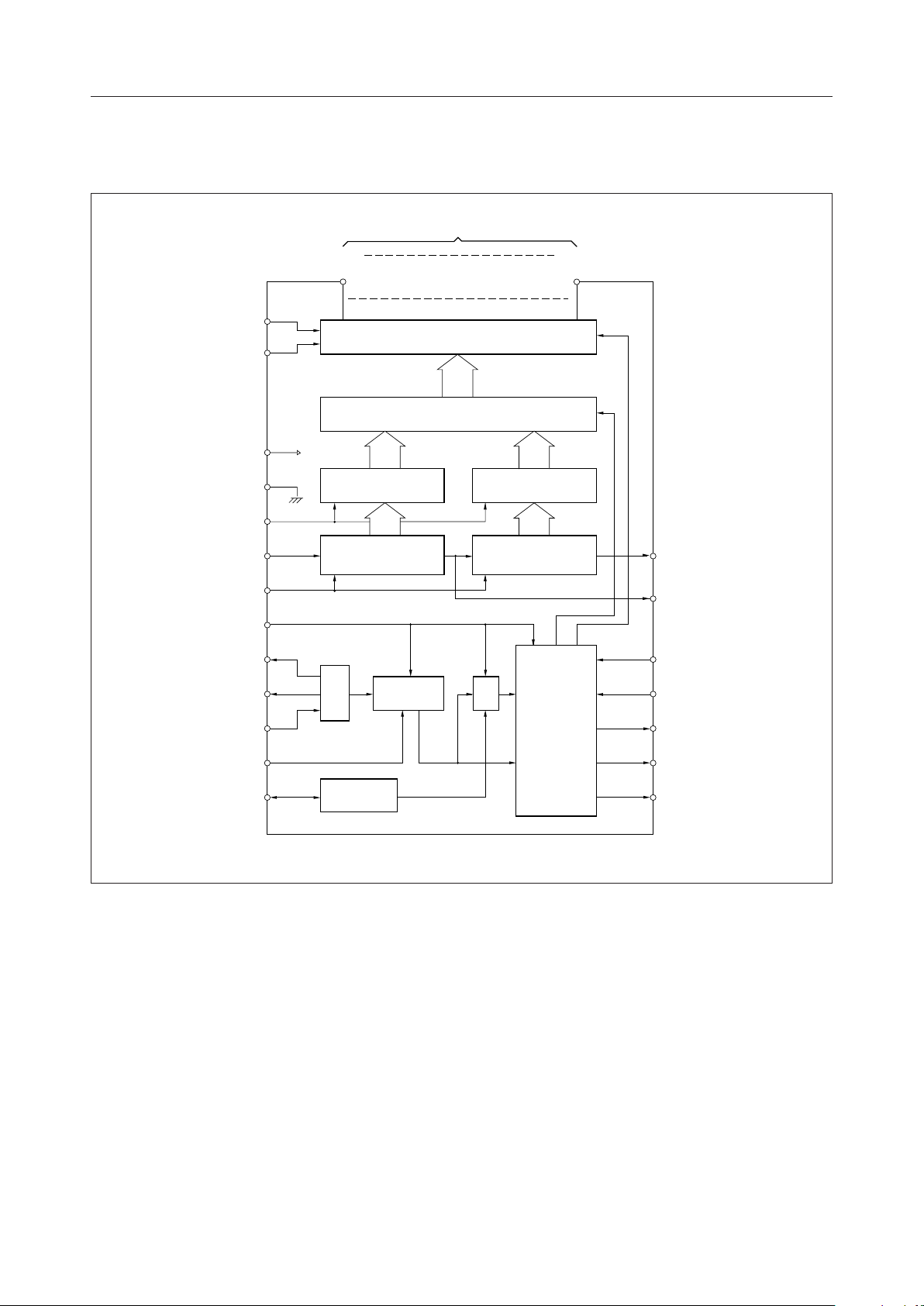
BLOCK DIAGRAM
MSM5265¡ Semiconductor
To LCD panel
SEG-TEST
BLANK
V
GND
LOAD
DATA-IN
CLOCK
D/S
OSC-OUT
OSC-OUT
OSC-IN
SEG
1
SEG
80
80-Dot Segment Driver
80
80-Ch Data Selector
DD
80-Stage Shift Register
80 80
(A)
80-Bit Data Latch
(A)
(B)
80-Bit Data Latch
(B)
80-Stage Shift Register
DATA-OUT 2
DATA-OUT 1
V
LC1
OSC 1/4 or 1/8 1/2
Common
Driver
V
LC2
COM-A
EXT/INT
SYNC
SYNC
Circuit
COM-B
COM-OUT
2/18
Page 3
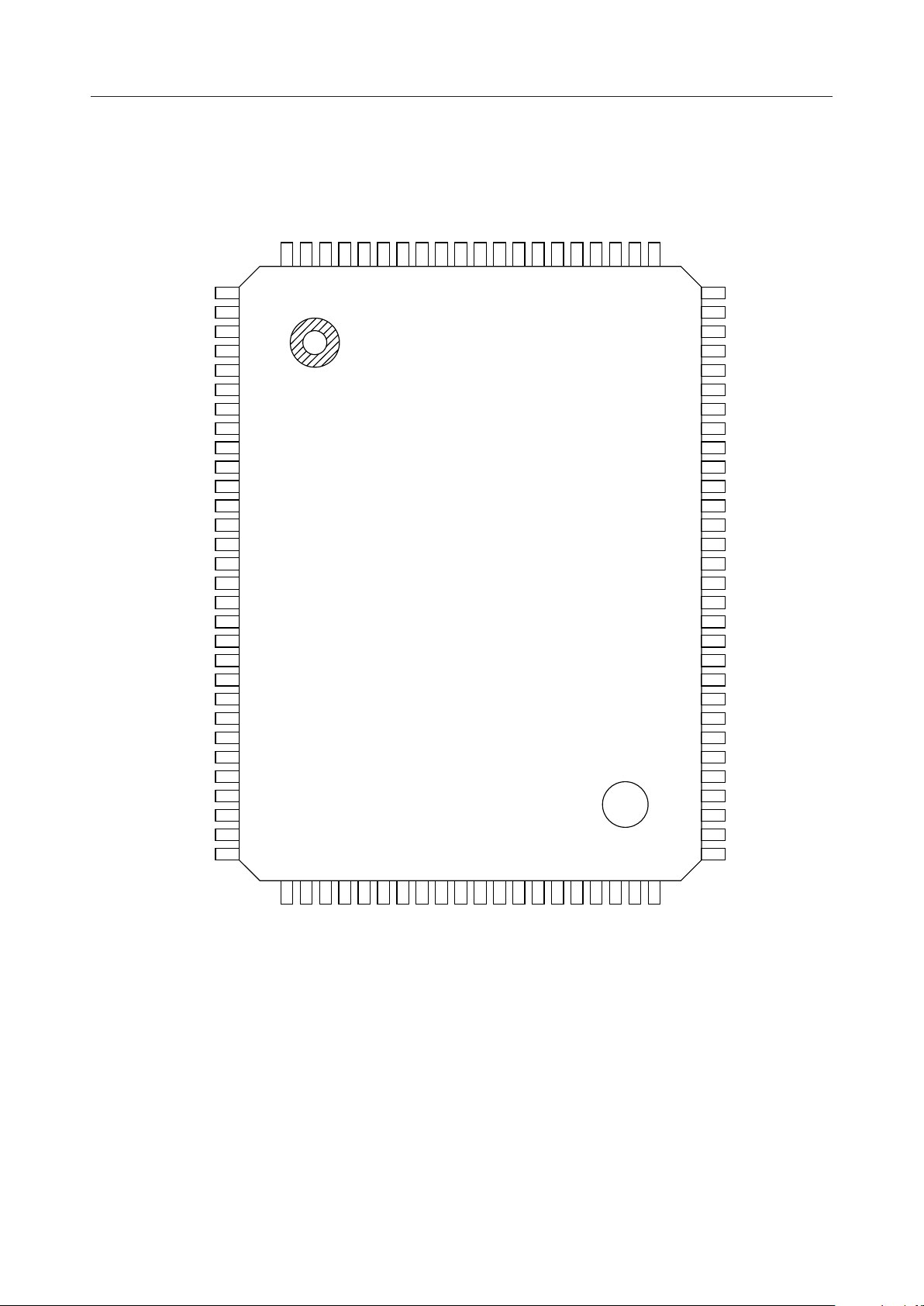
PIN CONFIGURATION (TOP VIEW)
SEG45
SEG46
SEG47
SEG48
SEG49
SEG50
95
96
97
98
99
100
SEG43
SEG44
93
94
SEG41
SEG42
91
92
SEG39
SEG40
89
90
SEG37
SEG38
87
88
SEG35
SEG36
85
86
SEG33
SEG34
83
84
SEG31
SEG32
81
82
MSM5265¡ Semiconductor
SEG51
SEG52
SEG53
SEG54
SEG55
SEG56
SEG57
SEG58
SEG59
SEG60
SEG61
SEG62
SEG63
SEG64
SEG65
SEG66
SEG67
SEG68
SEG69
SEG70
SEG71
SEG72
SEG73
SEG74
SEG75
SEG76
SEG77
SEG78
SEG79
SEG80
10
11
12
13
14
15
16
17
18
19
20
21
22
23
24
25
26
27
28
29
30
1
2
3
4
5
6
7
8
9
80
79
78
77
76
75
74
73
72
71
70
69
68
67
66
65
64
63
62
61
60
59
58
57
56
55
54
53
52
51
SEG30
SEG29
SEG28
SEG27
SEG26
SEG25
SEG24
SEG23
SEG22
SEG21
SEG20
SEG19
SEG18
SEG17
SEG16
SEG15
SEG14
SEG13
SEG12
SEG11
SEG10
SEG9
SEG8
SEG7
SEG6
SEG5
SEG4
SEG3
SEG2
SEG1
32
31
LOAD
CLOCK
34
33
DATA-IN
DATA-OUT1
42
41
40
39
38
37
36
35
DD
D/S
V
GND
OSC-IN
EXT/INT
OSC-OUT
OSC-OUT
DATA-OUT2
100-Pin Plastic QFP
45
44
43
SYNC
BLANK
SEG-TEST
48
47
46
LC1
V
COM-A
COM-OUT
50
49
LC2
V
COM-B
3/18
Page 4
ABSOLUTE MAXIMUM RATINGS
Parameter Symbol Condition Rating Unit
Supply Voltage
Input Voltage
Storage Temperature
T
V
DD
V
STG
I
= 25°C
T
a
= 25°C
T
a
—
RECOMMENDED OPERATING CONDITIONS
Parameter Symbol Condition Range Unit
Supply Voltage
Operating Temperature
LCD Driving Voltage
• Oscillation circuit
V
V
T
DD
op
LCD
—
—
VDD–V
LC2
–0.3 to +6.5 V
GND–0.3 to VDD +0.3
–55 to +150
3 to 6 V
–40 to +85
3 to V
DD
MSM5265¡ Semiconductor
V
°C
°C
V
Parameter Min.
Symbol Condition Typ. Max. UnitCorresponding pin
Oscillator Resistance
Oscillator Capacitance 0.001C
Current Limiting Resistance 0.56R
Common Signal Frequency 25f
R
0
COM
OSC-OUT
C
0
0
0
1
— 100 220 kWOSC-OUT
Film capacitor — 0.047 mFOSC-OUT
R1≥10 R
56R
0
1 2.2 MWOSC-IN
COM-A
COM-B
— — 150 Hz
(MSM5265)
OSC-OUT
R
1
OSC-IN
4/18
Page 5
ELECTRICAL CHARACTERISTICS
DC Characteristics
Parameter Symbol Condition Applicable pinMin. Typ. Max. Unit
MSM5265¡ Semiconductor
= 5.0 V Ta =–40 to +85°C)
(V
DD
"H" Input
Voltage
"L" Input
Voltage
Input
Leakage
Current
"H" Output
Voltage
"M" Output
Voltage
V
IH
—
36 — V
DD
V
SEG-TEST, BLANK,
V
IL
—
GND — 1.0 V
LOAD, DATA-IN, CLOCK,
D/S, EXT/INT, OSC-IN
I
IL
V
= 5.0 V/0 V
I
——±1mA
DATA-OUT1
V
OH
I
= –100 mA 4.5 — — V
O
DATA-OUT2
COM-OUT
= –200 mA 4.5 — — V
I
O
V
= 2.5 V, V
LC1
I
= –30 mA
O
V
= 2.5 V, V
LC1
I
= –150 mA
O
V
= 2.5 V, V
V
OM
LC1
I
= ±150 mA
O
LC2
LC2
LC2
= 0 V
= 0 V
= 0 V
4.8 — — V
4.8 — — V
2.3 — 2.7 V
OSC-OUT
OSC-OUT
SEG1-SEG
COM-A
COM-B
COM-A
COM-B
80
"L" Output
Voltage
Output
Leakage
Current
Segment
Output
Impedance
DATA-OUT1
V
OL
I
= 100 mA — — 0.5 V
O
DATA-OUT2
COM-OUT
I
= 200 mA — — 0.5 V
O
V
= 2.5 V, V
LC1
I
= 30 mA
O
V
= 2.5 V, V
LC1
I
= 150 mA
O
I
= 250 mA — — 0.8 V
O
LC2
LC2
= 0 V
= 0 V
— — 0.2 V SEG
— — 0.2 V
OSC-OUT
OSC-OUT
- SEG
1
COM-A
COM-B
SYNC
80
VO= 5 V
I
LO
R
SEG
when internal Tr is off
V
LC1
V
LC2
= (5+V
= 0 to 2 V
LC2
)/2
—— 5 mA
— — 10 kW
SYNC
SEG
- SEG
1
80
5/18
Page 6
MSM5265¡ Semiconductor
Parameter
Common Output
Impedance
Static Supply
Current
Symbol
R
COM
I
DD1
Dynamic Supply
Current
I
DD2
Switching Characteristics
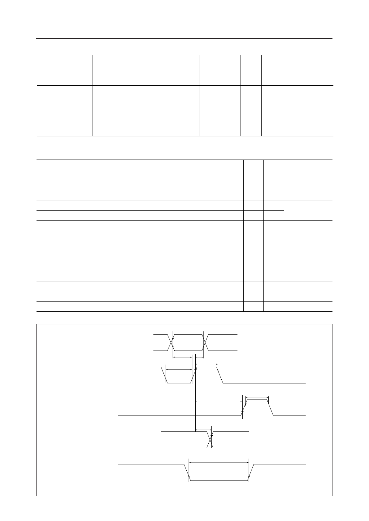
Parameter Symbol Condition Min. Max. Unit Applicable Pin
Clock Frequency f
Clock Pulse "H" Time f
Clock Pulse "L" Time f
Data Setup Time f
Data Hold Time f
"H"‚ "L" Propagation
Delay Time
LOAD Pulse "H" Time t
Clock Æ LOAD Time t
OSC-IN Input Frequency f
Condition Min. Typ. Max. Unit
= (5+V
V
LC1
V
= 0 to 2 V
LC2
Fix all input levels at
either V
or GND
DD
LC2
)/2
— — 1.5 kW
——
No load.
R
= 100 kW,
0
C
= 0.01 mF, R1 = 1 MW
0
—
(VDD = 3.0 to 6.0 V Ta = –40 to +85°C)
f
fH
fL
D–f
f–D
— — 1 MHz
— 0.3 — ms CLOCK
— 0.5 — ms
— 0.1 — ms DATA-IN
— 0.1 — ms
Load capacitance of
t
t
OSC
PHL
PLH
f–L
DATA-OUT1, DATA-OUT2:
L
— 0.8 ms
15 pF
— 0.2 — ms LOAD
— 0.1 — ms CLOCK
— — 5 kHz OSC-IN
100 mA
0.5 mA0.12
Applicable Pin
COM-A
COM-B
V
DD
CLOCK
DATA-OUT1
DATA-OUT2
CLOCK
LOAD
SYNC Pulse "L" Time t
DATA-IN
CLOCK
LOAD
DATA-OUT
DATA-OUT
SYNC
1
2
s
V
L
— 0.2 — ms SYNC
V
H
V
L
t
V
H
V
D-f
L
t
f-D
t
fH
= 0.8 V
H
V
H
V
L
t
t
f-L
V
H
V
L
t
s
V
= 0.2 VDD)
,
DD
L
L
V
H
V
L
V
H
V
L
V
H
V
L
t
PHL
t
PLH
V
L
(V
t
fL
6/18
Page 7

MSM5265¡ Semiconductor
FUNCTIONAL DESCRIPTION
Operational Description
The MSM5265 consists of a 160-stage shift register, 160-bit data latch, and 80 pairs of LCD
drivers. The display data is input from the DATA-IN pin to the 160-stage shift register at the
rising edge of the CLOCK pulse and it is shifted to the 160-bit data latch when the LOAD
signal is set at "H" level, then it is directly output from the 80 pairs of LCD drivers to the LCD
panel. Input the display data in the order of SEG80, SEG79, SEG78, ..., SEG2, SEG1.
DATA-IN
123456159160
CLOCK
LOAD
DATA LATCH
Output
(inside the IC)
Pin Functional Description
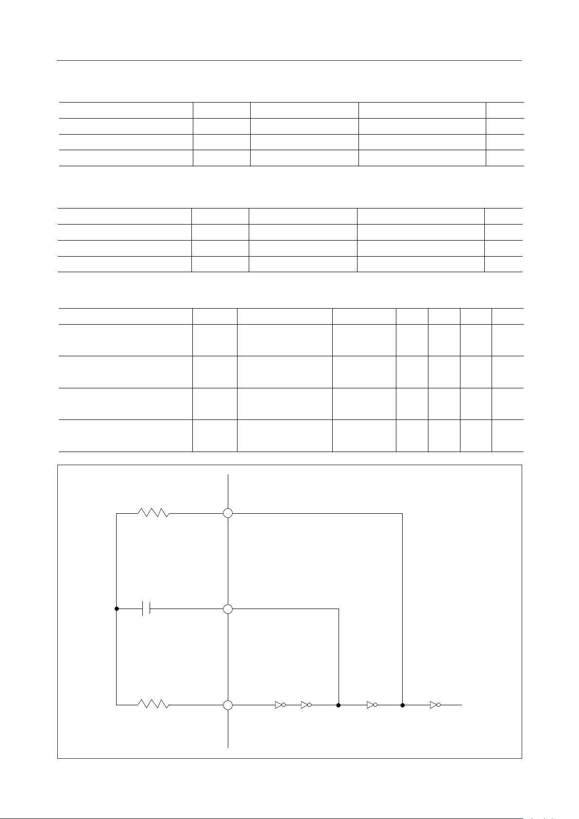
• OSC-IN, OSC-OUT, OSC-OUT
As shown in the figure below, by connecting the external resistors R0, R1 and external
capacitor C0 with OSC-IN, OSC-OUT and OSC-OUT respectively, an oscillating circuit to
generate the common signal is formed.
This frequency is divided into either 1/8 or 1/4 by the internal dividing circuit. The 1/8
divided frequency is used in the static display mode, while the 1/4 divided frequency is used
as the common signal in the 1/2 duty dynamic display mode which is output from the COMOUT pin. (EXT/INT should be set at low level.)
The resistor R1 is used to limit the current on the OSC-IN pin's protecting diodes. The value
of the R1 should be more than 10 times that of R0.
When the external common signal is used, the EXT/INT pin should be set at high level and
the external common signal should be input from the OSC-IN pin.
Keep the wiring between the OSC-IN pin and R1 as short as possible, because the OSC-IN pin
becomes susceptible to external noise if the value of R1 is large.
R
0
(MSM5265)
OSC-OUT
f
1/2.2 C0R
=
OSC
R
≥
C
0
OSC-OUT
V
DD
R
1
OSC-IN
1
10 R
0
0
f
OSC
7/18
Page 8

MSM5265¡ Semiconductor
• D/S
When this pin is set at high level, the MSM5265 operates in the 1/2 duty dynamic display
mode, the MSM5265 operates in the static display mode when this pin is set at low level.
• EXT/INT
When the external common signal is used, fix this pin at high level and input the external
common signal from the OSC-IN pin. The input common signal is used as the internal
common signal and is output from the COM-OUT pin through the buffer. When the built-in
common signal generator is used, fix this pin at low level. When the MSM5265 is used as an
output expander, fix this pin at high level and the OSC-IN pin at low level. The output logic
can be reveresed in respect to the input data by setting OSC-IN to "H" level.
• COM-OUT
When two or more MSM5265s are connected in series (cascade connection), this pin should
be connected with all of the slave MSM5265's OSC-IN pins.
• SYNC
This pin is an input/output pin which is used when two or more MSM5265s are connected
in series (cascade connection) in the 1/2 duty dynamic display mode. All of the involved
MSM5265's SYNC pins should be connected by the same line and they should be pulled up
with a common resistor, which makes a phase level of all involved MSM5265's COM-A and
COM-B pins equal. When a single MSM5265 is used in the dynamic display mode, SYNC
should be pulled up with a resistor.
Connect this pin to GND if any of the following conditions is true:
– the MSM5265 is operated in the static display mode
– two or more MSM5265 devices are cascade connected
– a single MSM5265 device is used
– the MSM5265 is used as an output expander
• DATA-IN, CLOCK
The display data is serially input from the DATA-IN pin to the 160-stage shift register at the
rising edge of the CLOCK pulse. The high level of the display data is used to turn the display
on, while low level of the display data is used to turn off the display.
• DATA-OUT1
The 80th stage of the shift register contents is output from this pin.
When two or more MSM5265s are connected in series (cascade connection) in the static
display mode, this pin should be connected to the next MSM5265's DATA-IN pin.
• DATA-OUT2
The 160th stage of the shift register contents is output from this pin.
When two or more MSM5265s are connected in series (cascade connection) in the 1/2 duty
dynamic display mode, this pin should be connected to the next MSM5265's DATA-IN pin.
• LOAD
The signal for latching the shift register contents is input from this pin.
When LOAD pin is set at high level, the shift register contents are shifted to the 80 sets of LCD
drivers. When this pin is set at low level, the last display data is held which was transfered
to the 80 sets of LCD drivers when LOAD pin was set at high level.
8/18
Page 9

MSM5265¡ Semiconductor
•V
LC2
Supply voltage pin for the 80 sets of LCD drivers. The input level to this pin should be the low
level output voltage of segment outputs (SEG1 to SEG80) and common outputs (COM-A,
COM-B).
In this case, the high level of segment outputs and common outputs is the VDD level, while
low level of segment outputs and common outputs is V
LC2
level. V
should be set at higher
LC2
level than ground level.
•V
LC1
Supply voltage pin for the middle level voltage of the common outputs. The input level of this
pin is the middle level output voltage of the common outputs (COM-A, COM-B) in the 1/2
duty dynamic display mode.
The value of V
V
LC1
is calculated by the following formula:
LC1
= (VDD + V
LC2
)/2
In the static display mode, this pin should be open.
• COM-A, COM-B
LCD driving common signals are output from these pins. These pins should be connected to
the common side of the LCD panel.
– In the static display mode
A pulse in phase with the COM-OUT output is output from both COM-A and COM-B. In
this case, the high level is V
and the low level is V
DD,
LC2
.
– In the 1/2 duty dynamic display mode
The COM-A and COM-B output signals are alternately changed within each COM-OUT
output cycle, resulting in alternate repetition of select and non-select modes.
In the select mode, a signal in phase with the COM-OUT signal is output at "H" (VDD) and
"L" (V
In the non-select mode, a voltage is output at "M" (V
LC2
).
). In the select mode of COM-A
LC1
(non-select mode of COM-B), signals that correspond to the 1st- to 80th-bit data of the data
latch are output to the segment outputs.
In the select mode of COM-B (non-select mode of COM-A), signals that correspond to the
81st- to 160th-bit data of the data latch are output to the segment outputs.
COM-OUT
COM-A
Dynamic display mode
(D/S : "H")
V
DD
V
LC1
V
LC2
Static display mode
(D/S : "L")
COM-B
V
DD
V
LC1
V
LC2
9/18
Page 10

MSM5265¡ Semiconductor
• SEG1 to SEG
80
LCD segment driving signals are output from these pins and they should be connected to the
segment side of the LCD panel.
"H" level : VDD, "L" level : V
LC2
– In the static display mode
The nth-bit data of the data latch (A) corresponds to the SEG n. The data of the data latch
(B) is invalid .
A signal out of phase with the COM-OUT signal is output to the segment outputs when the
display is turned on, while a signal in phase with it is output when the display is turned off.
– In the 1/2 duty dynamic display mode
Output of the SEG n corresponds to as follows.
When COM-A is in select mode:
nth-bit data of the data latch (A)
When COM-B is in select mode:
nth-bit data of the data latch (B)
When the display is turned on, a signal out of phase with the common signal corresponding
to the data is output, while a signal in phase with the common signal is output when the
display is turned off.
COM-A
COM-B
SEG n
Dynamic display mode
(D/S : "H")
Off Off Off Off
Off On Off On
On Off On Off
Static display mode
(D/S : "L")
COM-A
COM-B
Off
SEG n
On
On On On On
80+n 80+nnn
10/18
Page 11

MSM5265¡ Semiconductor
• SEG-TEST
This pin is used to test the segment outputs (SEG1 to SEG80). All displays are turned on when
this pin is set to high level. The display returns to the condition before the pin was set to high
level. When this pin is at high level, the input on the BLANK pin is disabled.
• BLANK
This pin is also used to test the segment outputs (SEG1 to SEG80). All displays are turned off
when this pin is set to high level. The display returns to the condition before the pin was set
to high level.
When SEG-TEST pin is at high level, the input on this pin is disabled.
11/18
Page 12

APPLICATION CIRCUITS
1) Single MSM5265 operation in the static display mode
MSM5265¡ Semiconductor
LCD panel
80 segments (static)
SEG
1
SEG
80
SEG-TEST
From
controller
BLANK
LOAD
MSM5265
DATA-IN
CLOCK
R
COM
D/S EXT/INT OSC-IN OSC-OUT
≥ 1.5 kW
OSC-OUT
R
1
1 MW 100 kW
C
0
0.01 mF
2) Single MSM5265 operation in the 1/2 duty dynamic display mode
R
0
COM
COM-A
V
LC2
SYNC
R
COM
V
DD
From
controller
R
≥ 1.5 kW, R
COM
LCD panel
80 x 2 segments (1/2 duty dynamic)
SEG
1
SEG
SEG-TEST
BLANK
LOAD
MSM5265
DATA-IN
CLOCK
D/S EXT/INT OSC-IN OSC-OUT
V
DD
≥ R
COM
LC
OSC-OUT
R
1
1 MW 100 kW
C
0
0.01 mF
COM-A
COM-B
80
V
LC1
COM-A
COM-B
V
LC2
SYNC
R
0
R
x 2
COM
V
22 k
V
DD
R
LC
R
LC
LC2
W
12/18
Page 13

3) Cascade connections for MSM5265s in the static display mode
MSM5265¡ Semiconductor
COM
R
COM
R
COM-A
COM-A
LC2
V
LC2
V
SYNC
DATA-OUT 1
DATA-IN
SYNC
DATA-OUT 1
OSC-IN D/S EXT/INT OSC-IN
LC2
V
DD
V
DD
V
1.5 kW
≥
COM
R
LCD panel (80 x n segments) static
COM
COM
R
80 80 80
MSM5265 MSM5265
LC2
V
COM-A
MSM5265
SEG-TEST
BLANK
DATA-IN
COM-OUT
DATA-OUT 1
LOAD
DATA-IN
D/S EXT/INT
SYNC
OSC
D/S EXT/INT
CLOCK
13/18
Page 14

4) Cascade connections for MSM5265s in the 1/2 duty dynamic display mode
COM
R
COM
R
LCI
V
COM-A
V
COM-B
LC2
SYNC
DATA-OUT 2
LC
R
≥
COM
1.5 kW, R
≥
COM
R
MSM5265¡ Semiconductor
COM
R
COM
R
LCI
V
COM-B
COM-A
MSM5265 MSM5265
COM-B
COM
R
COM-A
LCD panel (80 x n segments) 1/2 duty dynamic
COM
R
LCI
V
COM-A
COM-B
80 80 80
V
LC2
LC2
V
DATA-IN
DATA-OUT 2
DATA-IN
COM-OUT
DATA-OUT 2
SYNC
SYNC
OSC-IN D/S EXT/INT OSC-IN
D/S EXT/INT
OSC
DD
V
DD
V
DD
V
22kW
CLOCK
D/S EXT/INT
DD
V
MSM5265
DD
V
LC
LC
R
R
V
LC2
SEG-TEST
BLANK
LOAD
DATA-IN
14/18
Page 15

5) Output-expander
MSM5265¡ Semiconductor
80 outputs (same logic as input data)
From
controller
SEG-TEST
BLANK
LOAD
SEG
1
MSM5265
SEG
80
V
LC2
DATA-IN
CLOCK
SYNC
D/S EXT/INT OSC-IN
V
DD
*
* The output logic can be reversed with respect to the input data by setting OSC-IN to "H" level.
15/18
Page 16

REFERENCE DATA
I
vs. V
DD2
DD
m
A
300
I
DD2
200
100
0
0
Condition
Oscillating, no load
Room temperature
R0=100kW
=0.01mF
C
0
=1MW
R
1
1 234567
DD
V
V
MSM5265¡ Semiconductor
f
COM
f
OSC
vs. R0, C
vs. V
DD
0
Hz
320
280
240
f
COM
f
OSC
460
450
440
430
420
410
200
160
140
120
100
175
125
8.75
6.25
Hz
80
70
60
50
40
35
30
25
20
15
Condition
10
7.5
5
D/S="L"
EXT/INT="L"
V
=5.0V
DD
R1=10R
0
f
=1/8
f
COM
Room temperature
.
=1/ (17.6C0R0)
.
OSC
56 68 82 100 120 150 180 220
R
0
+2%
0%
–2%
Condition
Room temperature
R0=100kW
=0.01mF
C
0
=1MW
R
1
C0=0.001mF
C0=0.0022mF
=0.0047mF
C
0
C
=0.01mF
0
=0.022mF
C
0
C
=0.047mF
0
kW
1 234567
V
DD
V
16/18
Page 17

PACKAGE DIMENSIONS
QFP100-P-1420-0.65-K
Mirror finish
MSM5265¡ Semiconductor
(Unit : mm)
Package material
Lead frame material
Pin treatment
Solder plate thickness
Package weight (g)
Epoxy resin
42 alloy
Solder plating
5 mm or more
1.29 TYP.
Notes for Mounting the Surface Mount Type Package
The SOP, QFP, TSOP, SOJ, QFJ (PLCC), SHP and BGA are surface mount type packages, which
are very susceptible to heat in reflow mounting and humidity absorbed in storage.
Therefore, before you perform reflow mounting, contact Oki’s responsible sales person for the
product name, package name, pin number, package code and desired mounting conditions
(reflow method, temperature and times).
17/18
Page 18

QFP100-P-1420-0.65-BK
Mirror finish
MSM5265¡ Semiconductor
(Unit : mm)
Package material
Lead frame material
Pin treatment
Solder plate thickness
Package weight (g)
Epoxy resin
42 alloy
Solder plating
5 mm or more
1.29 TYP.
Notes for Mounting the Surface Mount Type Package
The SOP, QFP, TSOP, SOJ, QFJ (PLCC), SHP and BGA are surface mount type packages, which
are very susceptible to heat in reflow mounting and humidity absorbed in storage.
Therefore, before you perform reflow mounting, contact Oki’s responsible sales person for the
product name, package name, pin number, package code and desired mounting conditions
(reflow method, temperature and times).
18/18
 Loading...