

Page 1

E2B0016-27-Y2
¡ Semiconductor
This version: Nov. 1997
Previous version: Mar. 1996
MSM5260¡ Semiconductor
MSM5260
80-DOT COMMON/SEGMENT DRIVER
GENERAL DESCRIPTION
The MSM5260 is a dot matrix common/segment LCD driver LSI which is fabricated using low
power CMOS metal gate technology. This LSI consists of 80-bit shift register, 80-bit latch, 80-bit
level shifter and 80-bit 4-level driver.
It converts display data, which is serially received from an LCD controller LSI, to parallel data,
and outputs LCD driving waveform to LCD.
This LSI can drive a variety of LCD panels since the bias voltage can be optionally supplied from
an external source.
FEATURES
• Supply voltage : 4.5 to 5.5V
• LCD driving voltage : 8 to 18V
• Applicable LCD duty : static and 1/32 to 1/64
• Bias voltage can be supplied externally
• Can be used either as common or segment driver
• Interface with MSM6255 LCD controller LSI
• Package options :
100-pin plastic QFP (QFP100-P-1420-0.65-K) (Product name : MSM5260GS-K)
100-pin plastic QFP (QFP100-P-1420-0.65-L) (Product name : MSM5260GS-L)
100-pin plastic QFP (QFP100-P-1420-0.65-BK) (Product name : MSM5260GS-BK)
1/12
Page 2
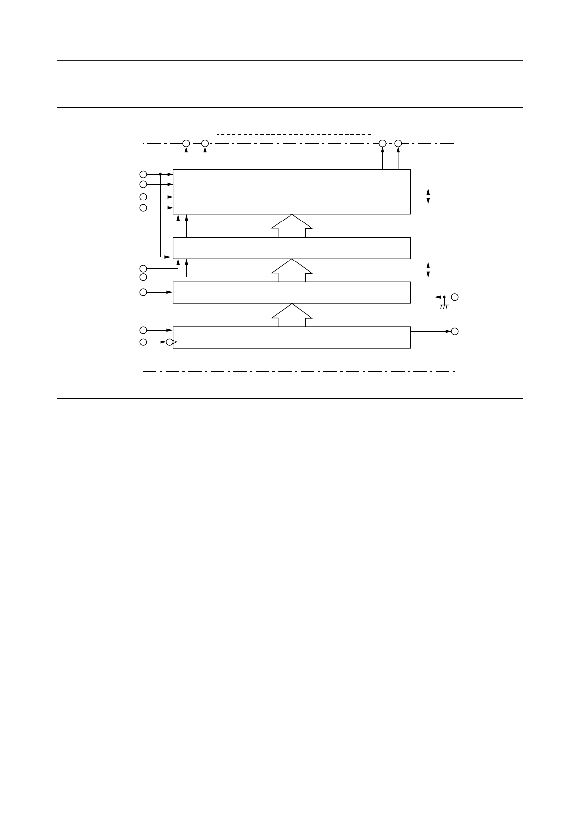
BLOCK DIAGRAM
MSM5260¡ Semiconductor
COM/SEG
LOAD
DI
V
V2
V
V
DF
1
CP
DD
O
O
1
2
3
5
80-Bit 4-Level Driver
80-Bit Level Shifter
80-Bit Latch
80-Bit Shift Register
O79O
80
VDD
V
5
V
DD
V
SS
V
SS
DO
80
2/12
Page 3
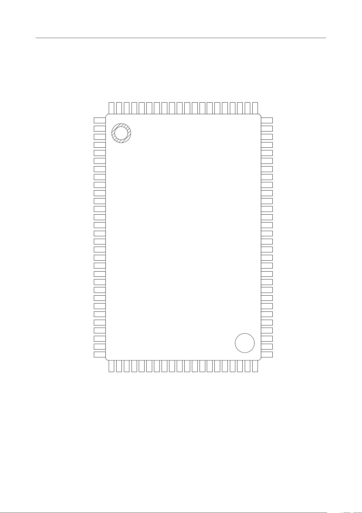
PIN CONFIGURATION (TOP VIEW)
MSM5260¡ Semiconductor
*
O1NC
100
1
O
2
O
2
3
O
3
4
O
4
5
O
5
6
O
6
7
O
7
8
8
O
9
9
O
10
O
10
11
11
O
12
12
O
13
13
O
14
O
14
15
O
15
16
16
O
17
17
O
18
18
O
19
O
19
20
O
20
21
21
O
22
22
O
23
23
O
24
O
24
25
O
25 56
26
O
26
27
O
27
28
O
28
29
O
29
30
O
30
31
DD
V3V
9998979695949392919089
CP
1
NC
NCNCNCNCDO80NC
DI
88
SS
LOAD
V
DFNCCOM/SEG
878685
5
V
V
838281
2
80
O
80
O
79
79
78
O
78
O
77
77
O
76
76
75
O
75
O
74
74
O
73
73
O
72
72
O
71
71
O
70
70
69
O
69
O
68
68
67
O
67
O
66
66
O
65
65
64
O
64
O
63
63
62
O
62
O
61
61
O
60
60
59
O
59
O
58
58
57
O
57
O
56
55
O
55
54
O
54
53
O
53
52
O
52
51
O
51
31323334353637383940414243
*
32
36
O34O33O
O35O
39
37
40
DD
O
O
O38O
V
O41O42O
444546
43
O44O45O
46
484950
47 84
47
O48O49O
O
NC : No connection
100-Pin Plastic QFP (Type K)
*VDD must be supplied to both pin 40 and pin 97.
50
3/12
Page 4
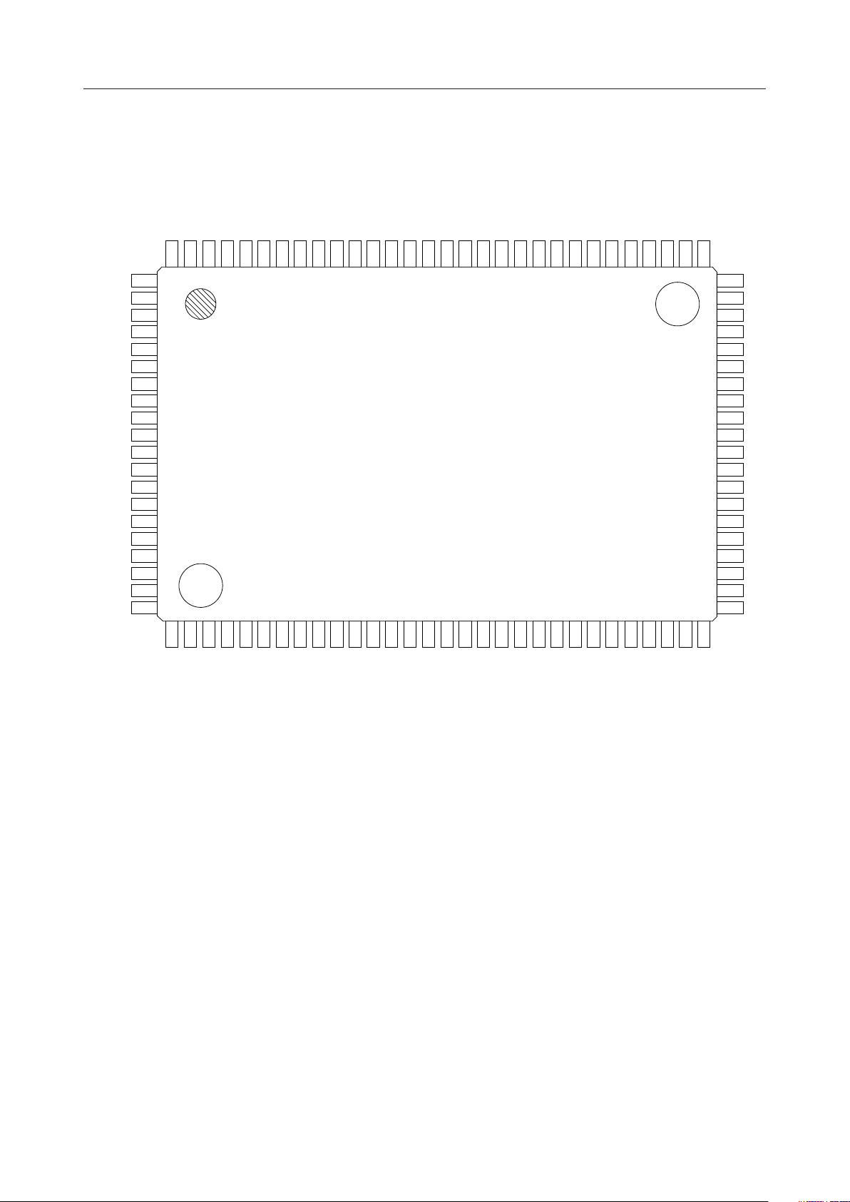
PIN CONFIGURATION
MSM5260¡ Semiconductor
O
NC
V
V
DD
CP
NC
DI
NC
NC
NC
NC
DO
80
NC
LOAD
V
SS
DF
NC
COM/SEG
V
V
15
O2O3O4O5O6O7O8O9O10O11O12O13O14O
2
1
100
1
4
3
5
6
7
8
9
1011121314
O16O17O18O19O
1516171819
20
O21O22O23O24O
2021222324
25
O26O27O28O
255626272829
99
98
3
*
97
96
95
94
1
93
92
91
90
89
88
87
86
85
84
83
82
5
81
2
79
80
O80O
77
78
767574737271706968676665646362
77
79
O78O76O75O74O73O72O71O70O69O68O
O
67
O66O65O64O63O
6160595857
62
O61O60O59O58O
5554535251
57
O56O55O54O53O52O
30
29
31
O
O
30
31
O
32
O
32
33
O
33
34
O
34
35
O
35
36
O
36
37
O
37
38
O
38
39
O
39
40
V
*
DD
40
O
41
41
O
42
42
O
43
43
O
44
44
O
45
45
O
46
46
O
47
47
O
48
48
O
49
49
O
50
50
51
NC : No connection
100-Pin Plastic QFP (Type L)
*VDD must be supplied to both pin 40 and pin 97.
Note: This figure shows the configuration viewed from the reverse side of the package. Pay
attention to the difference in pin arrangement.
4/12
Page 5

ABSOLUTE MAXIMUM RATINGS
Parameter Symbol Condition Rating Unit
MSM5260¡ Semiconductor
Supply Voltage (1)
Supply Voltage (2)
Input Voltage
Storage Temperature
*1 VDD > V2 > V3 > V
5
V
T
V
DD
LCD
V
STG
T
= 25°C
a
Ta = 25°C, V
= 25°C, V
T
a
T
I
a
–
DD
–
DD
= 25°C
V
*1
5
V
*1*2 0 to 20 V
5
—
–0.3 to +6.0
0 to 18
–0.3 to V
–55 to +150
*2 When a series resistance of more than 47W is connected as shown below:
V
DD
MSM5260
V
SS
V
2
V
3
V
5
R
≥47W
S
V
V
–
DD
5
+V
–V
DD
+0.3
V
V
V
°C
5/12
Page 6

RECOMMENDED OPERATING CONDITIONS
Parameter Symbol Condition Range Unit
MSM5260¡ Semiconductor
Supply Voltage (1)
Supply Voltage (2)
Operating Temperature
*1 VDD > V2 > V3 > V
5
V
DD
V
LCD
T
op
—
V
V
5
*1*2
5
*1
V
–
DD
V
–
DD
—
4.5 to 5.5
8 to 16
8 to 18
–20 to +85
*2 When a series resistance of more than 47W is connected as shown below:
V
DD
MSM5260
V
SS
V
2
V
3
V
5
R
≥47W
S
V
V
–
DD
5
+V
–V
V
V
V
°C
ELECTRICAL CHARACTERISTICS
DC Characteristics
Parameter
"H" Input Voltage
"L" Input Voltage
"H" Input Current
"L" Input Current
"H" Output Voltage
"L" Output Voltage
ON Resistance
Supply Current
Symbol Condition
*1
V
IH
*1
V
IL
*1
I
IH
*1
I
IL
*2
V
OH
*2
V
OL
*4
R
ON
I
DD
= V
IH
DD
= 0V
IL
= –0.4mA
O
= 0.4mA
O
V
V
CP
V
= 10V
DD–V5
= 0.25V *3
N–VO
= DC
= 18V, no load
DD–V5
*1 Applied to LOAD, CP, DI1, DF and COM/SEG
*2 Applied to DO
80
*3 VN = VDD to V5, V2 = 8/9 (VDD – V5), V3 = 1/9 (VDD – V5)
*4 Applied to O1 to O
80
Min.
0.8V
V
SS
——1V
——–1V
VDD – 0.4 — —I
— — 0.4I
—12
— — 100
DD
(V
= 5V ± 10%, Ta = –20 to +85°C)
DD
Typ. Max.
—V
— 0.2V
DD
DD
Unit
V
V
mA
mA
V
V
kW
mA
6/12
Page 7

Switching Characteristics
MSM5260¡ Semiconductor
(VDD = 5V ± 10%, Ta = –20 to +85°C, CL = 15pF)
Parameter
"H","L" Propagation Delay Time
Clock Frequency
Clock Pulse Width
LOAD Pulse Width
Data Setup Time DIÆCP
CPÆLOAD Time
LOADÆCP Time
Data Hold Time DIÆCP
CP Rise/Fall Time
LOAD Rise/Fall Time ms
t
w(CP)
Symbol Condition
t
pLH
t
pHL
f
CP
t
W(CP)
t
W(L)
t
SETUP
t
CL
t
LC
t
HOLD
t
(CP)
r
t
(CP)
f
t
(L)
r
t
(L)
f
t
f(CP)
t
w(CP)
Duty
—
= 50%
—
—
—
—
Min. Typ. Max.
——
—
125 —
125
50 — —
250 ——
0——
50 ——
——50
— — 1
t
r(CP)
—
——
250
3.3
—
—
—
—
—
Unit
ns
MH
ns
ns
ns
ns
ns
ns
ns
Z
CP
DI
1
DO
80
LOAD
0.8V
DD
t
SETUP
0.8V
DD
0.8V
0.2V
DD
DD
0.2V
0.8V
0.2V
t
t
DD
DD
PLH
PHL
DD
0.2V
t
t
HOLD
DD
r(L)
0.8V
0.2V
t
CL
0.8V
DD
DD
DD
0.8V
0.2V
t
w(L)
DD
0.8V
DD
t
SETUP
DD
0.8
V
0.2
V
t
f(L)
t
LC
0.2V
DD
DD
0.8V
DD
0.2V
0.8
0.2
DD
DD
t
HOLD
V
DD
V
DD
7/12
Page 8

MSM5260¡ Semiconductor
FUNCTIONAL DESCRIPTION
Pin Functional Description
•DI
1
The data input pin for the 80-bit shift register (between 1st to 80th bit). The display data is
clocked in to this pin. (Positive logic)
•CP
Clock pulse input pin for 80-bit shift register. The data is shifted to the 80-bit shift register at
the falling edge of the clock pulse. A data setup time (t
are required between a DI1 signal and a clock pulse.
Clock pulse rise time (tr) and clock pulse fall time (tf) should be a maximum of 50ns
respectively.
) and a data hold time (t
SETUP
HOLD
)
•DO
80
The 80th bit output from the 80-bit shift register.
The data which is input from DI1 is clocked out with the delay in the number of the bits of the
shift register.
When extending the number of characters, this pin is used to connect to the next MSM5260
in cascade.
• LOAD
The signal for latching the shift register contents is input from this pin.
When LOAD pin is set at "H" level, the shift register contents are transferred to the 80-bit 4level driver through the 80-bit level shifter.
When LOAD pin is set at "L" level, the last display output data (O1 to O80), which was
transferred when LOAD pin was at "H" level, is held.
•DF
Synchronous signal input pin for alternate signal for LCD driving.
8/12
Page 9

MSM5260¡ Semiconductor
• COM/SEG
Selection signal input pin. MSM5260 is used either as common driver or segment driver
according to input signal level at COM/SEG pin.
When this pin is set when at "H" level, MSM5260 is used as a common driver, while it is used
as a segment driver when at "L" level.
The display driving data O1 to O80 are determined according to the combination of latched
data and DF signal, as shown in Table 1 below.
Table 1
COM/SEG DF Remarks
H
L
Latched
data level
(Select)
Low
(Non-select)
High
(Select)
Low
(Non-select)
HHigh
L
H
L
H
L
H
L
Driver data output level
(O
O80)
-
1
V
DD
V
5
V
3
V
2
V
5
V
DD
V
3
V
2
Common driver
Segment driver
When MSM5260 is used as a common driver, both LOAD pin and COM/SEG pin are to be
connected to VDD. In this case, a bias voltage of common side’s non-select level is to be
supplied to V2 and V3 pins.
•VDD, V
SS
Supply voltage pins. VDD should be 4.5 to 5.5V.
VSS is a ground pin (VSS = 0V)
•V2, V3, V
5
Bias supply voltage pins to drive the LCD. Use an external bias voltage supply for driving
the LCD.
•O1 to O
80
Display data output pins which correspond to each bit of the 80-bit latch.
One of VDD, V2, V3 and V5 is selected as a display driving voltage source according to the
combination of latched data level and DF signal.
NOTES ON USE
Note the following when turning power on and off :
The LCD drivers of this IC requiers a high voltage. For this reason, if a high voltage is applied
to the LCD drivers with the logic power supply floating, excess current flows. This may damage
the IC. Be sure to carry out the following power-on and power-off sequences :
When turning power on :
First VDD ON, next V5, V3, V2 ON. Or both ON at the same time.
When turning power off :
First V5, V3, V2 OFF, next V
OFF. Or both OFF at the same time.
DD
9/12
Page 10

PACKAGE DIMENSIONS
QFP100-P-1420-0.65-K
Mirror finish
MSM5260¡ Semiconductor
(Unit : mm)
Package material
Lead frame material
Pin treatment
Solder plate thickness
Package weight (g)
Epoxy resin
42 alloy
Solder plating
5 mm or more
1.29 TYP.
Notes for Mounting the Surface Mount Type Package
The SOP, QFP, TSOP, SOJ, QFJ (PLCC), SHP and BGA are surface mount type packages, which
are very susceptible to heat in reflow mounting and humidity absorbed in storage.
Therefore, before you perform reflow mounting, contact Oki’s responsible sales person for the
product name, package name, pin number, package code and desired mounting conditions
(reflow method, temperature and times).
10/12
Page 11

QFP100-P-1420-0.65-L
Spherical surface
MSM5260¡ Semiconductor
(Unit : mm)
Package material
Lead frame material
Pin treatment
Solder plate thickness
Package weight (g)
Epoxy resin
42 alloy
Solder plating
5 mm or more
1.29 TYP.
Notes for Mounting the Surface Mount Type Package
The SOP, QFP, TSOP, SOJ, QFJ (PLCC), SHP and BGA are surface mount type packages, which
are very susceptible to heat in reflow mounting and humidity absorbed in storage.
Therefore, before you perform reflow mounting, contact Oki’s responsible sales person for the
product name, package name, pin number, package code and desired mounting conditions
(reflow method, temperature and times).
11/12
Page 12

QFP100-P-1420-0.65-BK
Mirror finish
MSM5260¡ Semiconductor
(Unit : mm)
Package material
Lead frame material
Pin treatment
Solder plate thickness
Package weight (g)
Epoxy resin
42 alloy
Solder plating
5 mm or more
1.29 TYP.
Notes for Mounting the Surface Mount Type Package
The SOP, QFP, TSOP, SOJ, QFJ (PLCC), SHP and BGA are surface mount type packages, which
are very susceptible to heat in reflow mounting and humidity absorbed in storage.
Therefore, before you perform reflow mounting, contact Oki’s responsible sales person for the
product name, package name, pin number, package code and desired mounting conditions
(reflow method, temperature and times).
12/12
 Loading...