

Datasheet MSM51V17805BSL-60JS, MSM51V17805B-70JS, MSM51V17805B-60JS, MSM51V17805BSL-70TS-K, MSM51V17805BSL-60TS-K Datasheet (OKI)
...Page 1
377
¡ Semiconductor MSM51V17805B/BSL
DESCRIPTION
The MSM51V17805B/BSL is a 2,097,152-word ¥ 8-bit dynamic RAM fabricated in Oki's silicon-gate
CMOS technology. The MSM51V17805B/BSL achieves high integration, high-speed operation, and
low-power consumption because Oki manufactures the device in a quadruple-layer polysilicon/
double-layer metal CMOS process. The MSM51V17805B/BSL is available in a 28-pin plastic SOJ or
28-pin plastic TSOP. The MSM51V17805BSL (the self-refresh version) is specially designed for
lower-power applications.
FEATURES
• 2,097,152-word ¥ 8-bit configuration
• Single 3.3 V power supply, ±0.3 V tolerance
• Input : LVTTL compatible, low input capacitance
• Output : LVTTL compatible, 3-state
• Refresh : 2048 cycles/32 ms, 2048 cycles/128 ms (SL version)
• Fast page mode with EDO, read modify write capability
• CAS before RAS refresh, hidden refresh, RAS-only refresh capability
• CAS before RAS self-refresh capability (SL version)
• Multi-bit test mode capability
• Package options:
28-pin 400 mil plastic SOJ (SOJ28-P-400-1.27)
(Product : MSM51V17805B/BSL-xxJS)
28-pin 400 mil plastic TSOP (TSOPII28-P-400-1.27-K)
(Product : MSM51V17805B/BSL-xxTS-K)
xx indicates speed rank.
PRODUCT FAMILY
¡ Semiconductor
MSM51V17805B/BSL
2,097,152-Word ¥ 8-Bit DYNAMIC RAM : FAST PAGE MODE TYPE WITH EDO
MSM51V17805B/BSL-70
70 ns
124 ns
84 ns
396 mW
540 mW
Family
Access Time (Max.)
Cycle Time
(Min.)
Standby (Max.)
Power Dissipation
MSM51V17805B/BSL-50
t
RAC
50 ns
35 ns
t
AA
25 ns
20 ns
t
CAC
13 ns
20 ns
t
OEA
13 ns
MSM51V17805B/BSL-60
60 ns
104 ns 468 mW
30 ns 15 ns 15 ns
Operating (Max.)
1.8 mW/
0.72 mW (SL version)
E2G0079-17-41
Page 2
378
MSM51V17805B/BSL ¡ Semiconductor
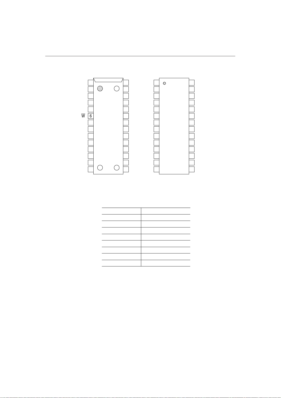
PIN CONFIGURATION (TOP VIEW)
3
4
5
9
10
11
12
13
DQ2
DQ3
DQ4
A10R
A0
A1
A2
A3
26
25
24
20
19
18
17
16
DQ7
DQ6
DQ5
A8
A7
A6
A5
A4
2
DQ1 27 DQ8
1
V
CC
28 V
SS
28-Pin Plastic SOJ
3
4
5
9
10
11
12
13
26
25
24
20
19
18
17
16
2
27
1
28
28-Pin Plastic TSOP
(K Type)
6WE 23 CAS 23
8NC 21 A9 21
6
8
7RAS 22 OE 227
14V
CC
15 V
SS
14 15
DQ2
DQ3
DQ4
A10R
A0
A1
A2
A3
DQ1
V
CC
WE
NC
RAS
V
CC
DQ7
DQ6
DQ5
A8
A7
A6
A5
A4
DQ8
V
SS
CAS
A9
OE
V
SS
Pin Name Function
A0 - A9, A10R
Address Input
RAS Row Address Strobe
CAS Column Address Strobe
DQ1 - DQ8 Data Input/Data Output
OE Output Enable
WE Write Enable
V
CC
Power Supply (3.3 V)
V
SS
Ground (0 V)
Note : The same power supply voltage must be provided to every VCC pin, and the same GND
voltage level must be provided to every VSS pin.
Page 3
379
¡ Semiconductor MSM51V17805B/BSL
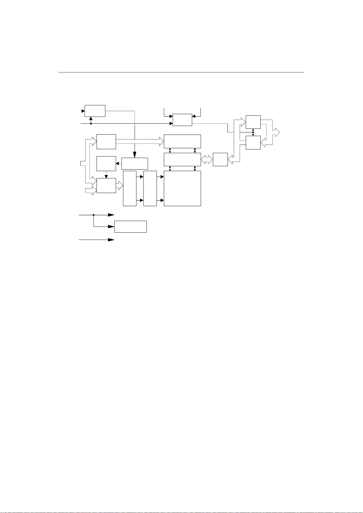
BLOCK DIAGRAM
Timing
Generator
Refresh
Control Clock
Column
Address
Buffers
Internal
Address
Counter
Row
Address
Buffers
Row
Decoders
Word
Drivers
Memory
Cells
Sense Amplifiers
Column Decoders
I/O
Controller
I/O
Selector
Output
Buffers
Input
Buffers
On Chip
V
BB
Generator
V
CC
DQ1 - DQ8
CAS
WE
A0 - A9
10 10
8
8
8
8
88
11
10
OE
RAS
V
SS
1
A10R
Page 4

380
MSM51V17805B/BSL ¡ Semiconductor
ELECTRICAL CHARACTERISTICS
Absolute Maximum Ratings
Recommended Operating Conditions
Capacitance
*: Ta = 25°C
Voltage on Any Pin Relative to V
SS
Short Circuit Output Current
Power Dissipation
Operating Temperature
Storage Temperature
V
T
Symbol
I
OS
P
D
*
T
opr
T
stg
–0.5 to 4.6
50
1
0 to 70
–55 to 150
Rating
mA
W
°C
°C
Parameter
V
Unit
Power Supply Voltage
Input High Voltage
Input Low Voltage
V
CC
Symbol
V
SS
V
IH
V
IL
3.3
0
—
—
Typ.Parameter
3.0
0
2.0
–0.3
Min.
3.6
0
V
CC
+ 0.3
0.8
Max.
(Ta = 0°C to 70°C)
V
Unit
V
V
V
Input Capacitance (A0 - A9, A10R)
Input Capacitance (RAS, CAS, WE, OE)
Output Capacitance (DQ1 - DQ8)
C
IN1
Symbol
C
IN2
C
I/O
5
7
7
Max.
pF
Unit
pF
pF
Parameter
(V
CC
= 3.3 V ±0.3 V, Ta = 25°C, f = 1 MHz)
—
—
—
Typ.
Page 5

381
¡ Semiconductor MSM51V17805B/BSL
DC Characteristics
Parameter
Symbol
Condition
MSM51V17805
B/BSL-50
MSM51V17805
B/BSL-60
MSM51V17805
B/BSL-70
(VCC = 3.3 V ±0.3 V, Ta = 0°C to 70°C)
IOH = –2.0 mAOutput High Voltage
IOL = 2.0 mAOutput Low Voltage
0 V £ VI £ VCC + 0.3 V;
All other pins notInput Leakage Current
under test = 0 V
DQ disable
Output Leakage Current
0 V £ VO £ V
CC
RAS, CAS cycling,
Average Power
t
RC
= Min.
Supply Current
(Operating)
RAS, CAS = V
IH
Power Supply
RAS, CAS
Current (Standby)
RAS cycling,Average Power
CAS = V
IH
,Supply Current
tRC = Min.(RAS-only Refresh)
RAS = V
IH
,
Power Supply
CAS = V
IL
,
Current (Standby)
DQ = enable
Average Power
CAS before RAS
Supply Current
(CAS before RAS Refresh)
Average Power
RAS £ 0.2 V,Supply Current
CAS £ 0.2 V(CAS before RAS
V
OH
V
OL
I
LI
I
LO
I
CC1
I
CC2
I
CC3
I
CC5
I
CC6
I
CCS
≥ VCC –0.2 V
Min. Max. Min. Max. Min. Max.
Unit Note
RAS cycling,
2.4
0
–10
–10
—
—
—
—
—
—
—
V
CC
0.4
10
10
150
2
0.5
150
150
300
5
2.4
0
–10
–10
—
—
—
—
—
—
—
V
CC
0.4
10
10
130
2
0.5
130
130
300
5
2.4
0
–10
–10
—
—
—
—
—
—
—
V
CC
0.4
10
10
110
2
0.5
110
110
300
5
— 200 — 200 — 200
V
V
mA
mA
mA
mA
mA
mA
mA
mA
1, 2
1, 2
1, 2
1, 5
1
1
mA 1, 5
tRC = 62.5 ms,Average Power
CAS before RAS,Supply Current
t
RAS
£ 1 ms(Battery Backup)
I
CC10
— 300 — 300 — 300 mA
1, 4,
RAS = VIL,Average Power
CAS cycling,Supply Current
t
HPC
= Min.(Fast Page Mode)
I
CC7
— 150 — 130 — 110 mA 1, 3
5
Self-Refresh)
Notes : 1. ICC Max. is specified as ICC for output open condition.
2. The address can be changed once or less while RAS = VIL.
3. The address can be changed once or less while CAS = VIH.
4. VCC – 0.2 V £ VIH £ VCC + 0.3 V, –0.3 V £ VIL £ 0.2 V.
5. SL version.
Page 6

382
MSM51V17805B/BSL ¡ Semiconductor
AC Characteristics (1/2)
Parameter
MSM51V17805
B/BSL-60
MSM51V17805
B/BSL-70
MSM51V17805
B/BSL-50
(VCC = 3.3 V ±0.3 V, Ta = 0°C to 70°C) Note 1, 2, 3, 12, 13
Random Read or Write Cycle Time
Read Modify Write Cycle Time
Fast Page Mode Cycle Time
Fast Page Mode Read Modify Write
Cycle Time
Access Time from RAS
Access Time from CAS
Access Time from Column Address
Access Time from CAS Precharge
CAS to Data Output Buffer Turn-off Delay Time
Transition Time
RAS Precharge Time
RAS Pulse Width
RAS Pulse Width (Fast Page Mode with EDO)
RAS Hold Time
CAS Pulse Width
CAS Hold Time
RAS to CAS Delay Time
RAS to Column Address Delay Time
CAS to RAS Precharge Time
Row Address Set-up Time
Row Address Hold Time
Column Address Set-up Time
Column Address Hold Time
Column Address to RAS Lead Time
Access Time from OE
OE to Data Output Buffer Turn-off Delay Time
Refresh Period
RAS Hold Time referenced to OE
Unit
Min. Max. Min. Max.
RAS Hold Time from CAS Precharge
Symbol
t
RC
t
RWC
t
HPC
t
HPRWC
t
RAC
t
CAC
t
AA
t
CPA
t
CEZ
t
T
t
RP
t
RAS
t
RASP
t
RSH
t
CAS
t
CSH
t
RCD
t
RAD
t
CRP
t
ASR
t
RAH
t
ASC
t
CAH
t
RAL
t
OEA
t
OEZ
t
REF
t
ROH
t
RHCP
Note
Min. Max.
Output Low Impedance Time from CAS t
CLZ
CAS Precharge Time (Fast Page Mode with EDO)
t
CP
4, 5, 6
4, 5
4, 6
4
7, 8
5
6
4
7
4
3
14
ns
ns
ns
ns
ns
ns
ns
ns
ns
ns
ns
ns
ns
ns
ns
ns
ns
ns
ns
ns
ns
ns
ns
ns
ns
ns
ns
ns
ms
ns
ns
84
110
20
58
—
—
—
—
0
0
1
30
50
50
7
7
7
35
11
9
5
0
7
0
7
25
—
0
—
7
30
—
—
—
—
50
13
25
30
—
13
50
—
10,000
100,000
—
—
10,000
—
37
25
—
—
—
—
—
—
13
13
32
—
—
124
160
30
78
—
—
—
—
0
0
1
50
70
70
13
10
13
45
14
12
5
0
10
0
13
35
—
0
—
13
40
—
—
—
—
70
20
35
40
—
20
50
—
10,000
100,000
—
—
10,000
—
50
35
—
—
—
—
—
—
20
20
32
—
—
104
135
25
68
—
—
—
—
0
0
1
40
60
60
10
10
10
40
14
12
5
0
10
0
10
30
—
0
—
10
35
—
—
—
—
60
15
30
35
—
15
50
—
10,000
100,000
—
—
10,000
—
45
30
—
—
—
—
—
—
15
15
32
—
—
Refresh Period (SL version)
t
REF
ms— 128 — 128— 128
Data Output Hold After CAS Low
WE to Data Output Buffer Turn-off Delay Time
RAS to Data Output Buffer Turn-off Delay Time
t
DOH
t
WEZ
t
REZ
7, 8
7
ns
ns
ns
5— 5—5—
OE Hold Time from CAS (DQ Disable)
t
CHO
ns5— 5—5—
0
0
13
13
0
0
20
20
0
0
15
15
Page 7

383
¡ Semiconductor MSM51V17805B/BSL
AC Characteristics (2/2)
MSM51V17805
B/BSL-60
MSM51V17805
B/BSL-70
MSM51V17805
B/BSL-50
Write Command Pulse Width
Write Command to CAS Lead Time
Write Command to RAS Lead Time
Data-in Set-up Time
CAS to WE Delay Time
RAS to WE Delay Time
Column Address to WE Delay Time
RAS to CAS Hold Time (CAS before RAS)
CAS Active Delay Time from RAS Precharge
Data-in Hold Time
Write Command Hold Time
OE Command Hold Time
OE to Data-in Delay Time
(VCC = 3.3 V ±0.3 V, Ta = 0°C to 70°C) Note 1, 2, 3, 12, 13
Write Command Set-up Time
t
WP
t
CWL
t
RWL
t
DS
t
CWD
t
RWD
t
AWD
t
CHR
t
RPC
t
DH
t
WCH
t
OEH
t
OED
t
WCS
Min. Max.
Parameter
Symbol
Unit Note
Min. Max. Min. Max.
RAS to CAS Set-up Time (CAS before RAS)t
CSR
WE to RAS Precharge Time (CAS before RAS)
t
WRP
WE Hold Time from RAS (CAS before RAS)t
WRH
RAS to WE Set-up Time (Test Mode) t
WTS
CAS Precharge WE Delay Time t
CPWD
RAS to WE Hold Time (Test Mode) t
WTH
11
10
10
10
11
10
10
10
10
10
10
10
0
34
79
49
5
10
5
10
10
15
0
54
—
—
—
—
—
—
—
—
—
—
—
—
—
—
—
—
—
ns
ns
ns
ns
ns
ns
ns
ns
ns
ns
ns
ns
ns
ns
ns
ns
ns
ns
ns
ns
10
10
10
10
7
0
30
67
42
5
10
5
7
7
13
0
47
—
—
—
—
—
—
—
—
—
—
—
—
—
—
—
—
—
10
10
10
10
10
0
44
94
59
5
10
5
13
13
20
0
64
—
—
—
—
—
—
—
—
—
—
—
—
—
—
—
—
—
—
—
—
RAS Pulse Width
t
RASS
14100 — ms100 — 100 —
(CAS before RAS Self-Refresh)
RAS Precharge Time
t
RPS
14110 — ns90 — 130 —
(CAS before RAS Self-Refresh)
CAS Hold Time
t
CHS
14–50 — ns–50 — –50 —
(CAS before RAS Self-Refresh)
Read Command Set-up Time
Read Command Hold Time
Read Command Hold Time referenced to RAS
t
RCS
t
RCH
t
RRH
9
9
ns
ns
ns
0
0
0
—
—
—
0
0
0
—
—
—
0
0
0
—
—
—
WE Pulse Width (DQ Disable) t
WPE
ns—
OE Command Hold Time
t
OCH
ns—
OE Precharge Time
t
OEP
ns—
10 —7— 10
10 —7— 13
10 —7— 10
10 —7— 10
10 —7— 13
10 —7— 13
Page 8

384
MSM51V17805B/BSL ¡ Semiconductor
Notes: 1. A start-up delay of 200 µs is required after power-up, followed by a minimum of eight
initialization cycles (RAS-only refresh or CAS before RAS refresh) before proper device
operation is achieved.
2. The AC characteristics assume tT = 2 ns.
3. VIH (Min.) and VIL (Max.) are reference levels for measuring input timing signals.
Transition times (tT) are measured between VIH and VIL.
4. This parameter is measured with a load circuit equivalent to 1 TTL load and 100 pF.
The output timing reference levels are VOH = 2.0 V and VOL = 0.8 V.
5. Operation within the t
RCD
(Max.) limit ensures that t
RAC
(Max.) can be met.
t
RCD
(Max.) is specified as a reference point only. If t
RCD
is greater than the specified
t
RCD
(Max.) limit, then the access time is controlled by t
CAC
.
6. Operation within the t
RAD
(Max.) limit ensures that t
RAC
(Max.) can be met.
t
RAD
(Max.) is specified as a reference point only. If t
RAD
is greater than the specified
t
RAD
(Max.) limit, then the access time is controlled by tAA.
7. t
CEZ
(Max.), t
REZ
(Max.), t
WEZ
(Max.) and t
OEZ
(Max.) define the time at which the
output achieves the open circuit condition and are not referenced to output voltage
levels.
8. t
CEZ
and t
REZ
must be satisfied for open circuit condition.
9. t
RCH
or t
RRH
must be satisfied for a read cycle.
10. t
WCS
, t
CWD
, t
RWD
, t
AWD
and t
CPWD
are not restrictive operating parameters. They are
included in the data sheet as electrical characteristics only. If t
WCS
≥ t
WCS
(Min.), then
the cycle is an early write cycle and the data out will remain open circuit (high
impedance) throughout the entire cycle. If t
CWD
≥ t
CWD
(Min.) , t
RWD
≥ t
RWD
(Min.),
t
AWD
≥ t
AWD
(Min.) and t
CPWD
≥ t
CPWD
(Min.), then the cycle is a read modify write
cycle and data out will contain data read from the selected cell; if neither of the above
sets of conditions is satisfied, then the condition of the data out (at access time) is
indeterminate.
11. These parameters are referenced to the CAS leading edge in an early write cycle, and
to the WE leading edge in an OE control write cycle, or a read modify write cycle.
12. The test mode is initiated by performing a WE and CAS before RAS refresh cycle.
This mode is latched and remains in effect until the exit cycle is generated.
The test mode specified in this data sheet is a 2-bit parallel test function. CA9 is not
used. In a read cycle, if all internal bits are equal, the DQ pin will indicate a high
level. If any internal bits are not equal, the DQ pin will indicate a low level.
The test mode is cleared and the memory device returned to its normal operating
state by performing a RAS-only refresh cycle or a CAS before RAS refresh cycle.
13. In a test mode read cycle, the value of access time parameters is delayed for 5 ns for the
specified value. These parameters should be specified in test mode cycle by adding the
above value to the specified value in this data sheet.
14. Only SL version.
See ADDENDUM O for AC Timing Waveforms
 Loading...