

Datasheet MSM5117800D-50TS-K, MSM5117800D-70TS-L, MSM5117800D-60TS-L, MSM5117800D-50TS-L, MSM5117800D-50JS Datasheet (OKI)
...Page 1
1/14
Semiconductor
M SM5117800D
2,097,152-Word
´´´´
8-Bit DYNA MIC RAM : FAST PAGE MODE TY PE
DESCRIPTION
The MSM5117800D is a 2,097,152-word ´ 8-bit dynamic RAM fabricated in Oki’s silicon-gate CMOS
technology. The MSM5117800D achieves high integration, high-speed operation, and low-power consumption
because Oki manufactures the device in a quadruple-layer polysilicon/double-layer metal CMOS process. The
MSM5117800D is available in a 28-pin plastic SOJ, 28-pin plastic TSOP.
FEATURES
·
2,097,152-word ´ 8-bit configuration
·
Single 5V power supply, ±10% tolerance
·
Input : TTL compatible, low input capacitance
· Output : TTL compatible, 3-state
· Refresh : 2048 cycles/32 ms
· Fast page mode, read modify write capability
·
CAS before RAS refresh, hidden refresh, RAS-only refresh capability
· Multi-bit test mode capability
· Package options:
28-pin 400mil plastic SOJ (SOJ28-P-400-1.27) (Product : MSM5117800D-xxJS)
28-pin 400mil plastic TSOP (TSOPII28-P-400-1.27-K) (Product : MSM5117800D-xxTS-K)
(TSOPII28-P-400-1.27-L) (Product : MSM5117800D-xxTS-L)
xx : indicates speed rank.
PRODUCT FAMILY
Access Time (Max.) Power Dissipation
Family
t
RAC
t
AA
t
CAC
t
OEA
Cycle Time
(Min.)
Operating (Max.) Standby (Max.)
MSM5117800D-50 50ns 25ns 13ns 13ns 90ns 550mW
MSM5117800D-60 60ns 30ns 15ns 15ns 110ns 495mW
MSM5117800D-70 70ns 35ns 20ns 20ns 130ns 440mW
5.5mW
This version:Apr.1999
Page 2
MSM5117800D
2/14
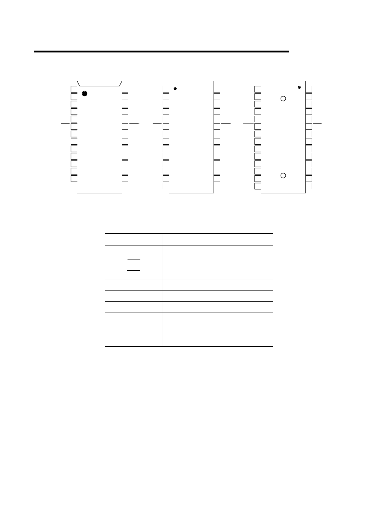
PIN CONFIGRATION (TOP VIEW)
Pin Name Function
A0–A9, A10R Address Input
RAS Row Address Strobe
CAS Column Address Strobe
DQ1–DQ8 Data Input/Data Output
OE Output Enable
WE Write Enable
V
CC
Power Supply (5V)
V
SS
Ground (0V)
NC No Connection
28-Pin Plastic SOJ
28-Pin Plastic TSOP
(L T
y
pe)
1
2
3
4
5
6
7
9
10
11
12
13
26
25
24
23
22
21
19
18
17
16
15
27DQ1
DQ2
V
CC
V
CC
V
SS
V
SS
DQ6
A8
A7
A6
A10R
A1
A2
A3
WE
RAS
NC
DQ3
A5
A4
OE
DQ8
DQ7
CAS
8
DQ4
20
A9
14
A0
DQ5
281
2
3
4
5
6
7
9
10
11
12
13
26
25
24
23
22
21
19
18
17
16
15
27DQ1
DQ2
V
CC
V
CC
V
SS
V
SS
DQ6
A8
A7
A6
A10R
A1
A2
A3
WE
RAS
NC
DQ3
A5
A4
OE
DQ8
DQ7
CAS
8
DQ4
20
A9
14
A0
DQ5
28
1
2
3
4
5
6
8
9
10
11
12
13
28
27
26
23
22
21
19
18
17
16
15
20
DQ1
DQ2
V
CC
V
CC
V
SS
V
SS
DQ8
DQ7
A9
A8
A7
A6
A0
A1
A2
A3
WE
RAS
NC
A10R
A5
A4
CAS
OE
7
DQ4
14
DQ3
25
24
DQ6
DQ5
28-Pin Plastic TSOP
(K T
y
pe)
Page 3
MSM5117800D
3/14
BLOCK DIAGRAM
A
0 – A9
8
8
8
10
11
10
Timing
Generator
Column
Address
Buffers
Internal
Address
Counter
Row
Address
Buffers
Refresh
Control Clock
Column Decoders
Sense Amplifiers
Memory
Cells
Word
Drivers
Row
Deco-
ders
I/O
Selector
Input
Buffers
Output
Buffers
DQ1 – DQ
8
OE
WE
RAS
CAS
VCCV
SS
On Chip
V
BB
Generator
I/O
Controller
On Chip
IV
CC
Generator
8
8
8
10
A10R
1
Page 4
MSM5117800D
4/14
ELECTRICAL CHARACTERISTICS
Absolute Maximum Ratings
Parameter Symbol Rating Unit
Voltage on Any Pin Relative to V
SS
VIN, V
OUT
-
0.5 to V
CC
+ 0.5
V
Voltage VCC supply Relative to V
SS
V
CC
0.5 to 7.0 V
Short Circuit Output Current
I
OS
50 mA
Power Dissipation
P
D*
1W
Operating Temperature
T
opr
0 to 70 °C
Storage Temperature
T
stg
-
55 to 150
°C
*: Ta = 25°C
Recommended Operating Conditions
(Ta = 0°C to 70°C)
Parameter Symbol Min. Typ. Max. Unit
V
CC
4.5 5.0 5.5 V
Power Supply Voltage
V
SS
000V
Input High Voltage
V
IH
2.4
¾
V
CC
+
0.5
*1
V
Input Low Voltage
V
IL
-
0.5
*2
¾
0.8 V
Notes: *1. The input voltage is VCC + 2.0V when the pulse width is less than 20ns (the pulse width is with
respect to the point at which V
CC
is applied).
*2. The input voltage is V
SS
- 2.0V when the pulse width is less than 20ns (the pulse width respect to
the point at which V
SS
is applied).
Capacitance
(VCC = 5V ± 10%, Ta = 25°C, f=1MHz )
Parameter Symbol Typ. Max. Unit
Input Capacitance (A0 – A9, A10R)
C
IN1
¾
5pF
Input Capacitance
(RAS, CAS, WE, OE)
C
IN2
¾
7pF
Output Capacitance (DQ1 – DQ8)
C
I/O
¾
7pF
Page 5
MSM5117800D
5/14
DC Characteristics
(VCC = 5V ± 10%, Ta = 0°C to 70°C)
MSM5117800
D-50
MSM5117800
D-60
MSM5117800
D-70
Parameter
Symbol
Condition
Min.
Max
Min.
Max
Min.
Max
Unit Note
Output High Voltage
V
OH
IOH = -5.0mA
2.4 V
CC
2.4 V
CC
2.4 V
CC
V
Output Low Voltage
V
OLIOL
= 4.2mA
00.400.400.4V
Input Leakage
Current
I
LI
0V £ VI £ 6.5V ;
All other pins not
under test = 0V
-
10
10
-
10
10
-
10
10
m
A
Output Leakage
Current
I
LO
DQ disable
0V £ V
O
£ V
CC
-
10
10
-
10
10
-
10
10
m
A
Average Power
Supply Current
(Operating)
I
CC1
RAS, CAS cycling,
t
RC
= Min.
¾
100
¾
90
¾
80 mA 1,2
RAS, CAS = V
IH
¾
2
¾
2
¾
2
Power Supply
Current
(Standby)
I
CC2
RAS, CAS
³
V
CC
– 0.2V
¾
1
¾
1
¾
1
mA 1
Average Power
Supply Current
(RAS-only Refresh)
I
CC3
RAS cycling,
CAS = V
IH
,
t
RC
= Min.
¾
100
¾
90
¾
80 mA 1,2
Power Supply
Current
(Standby)
I
CC5
RAS = VIH,
CAS = V
IL
,
DQ = enable
¾
5
¾
5
¾
5mA1
Average Power
Supply Current
(CAS before RAS
Refresh)
I
CC6
RAS = cycling,
CAS before RAS
¾
100
¾
90
¾
80 mA 1,2
Average Power
Supply Current
(Fast Page Mode)
I
CC7
RAS = VIL,
CAS cycling,
t
PC
= Min.
¾
80
¾
70
¾
60 mA 1,3
Notes: 1. ICC Max. is specified as ICC for output open condition.
2. The address can be changed once or less while RAS = V
IL
.
3. The address can be changed once or less while CAS = V
IH
.
Page 6

MSM5117800D
6/14
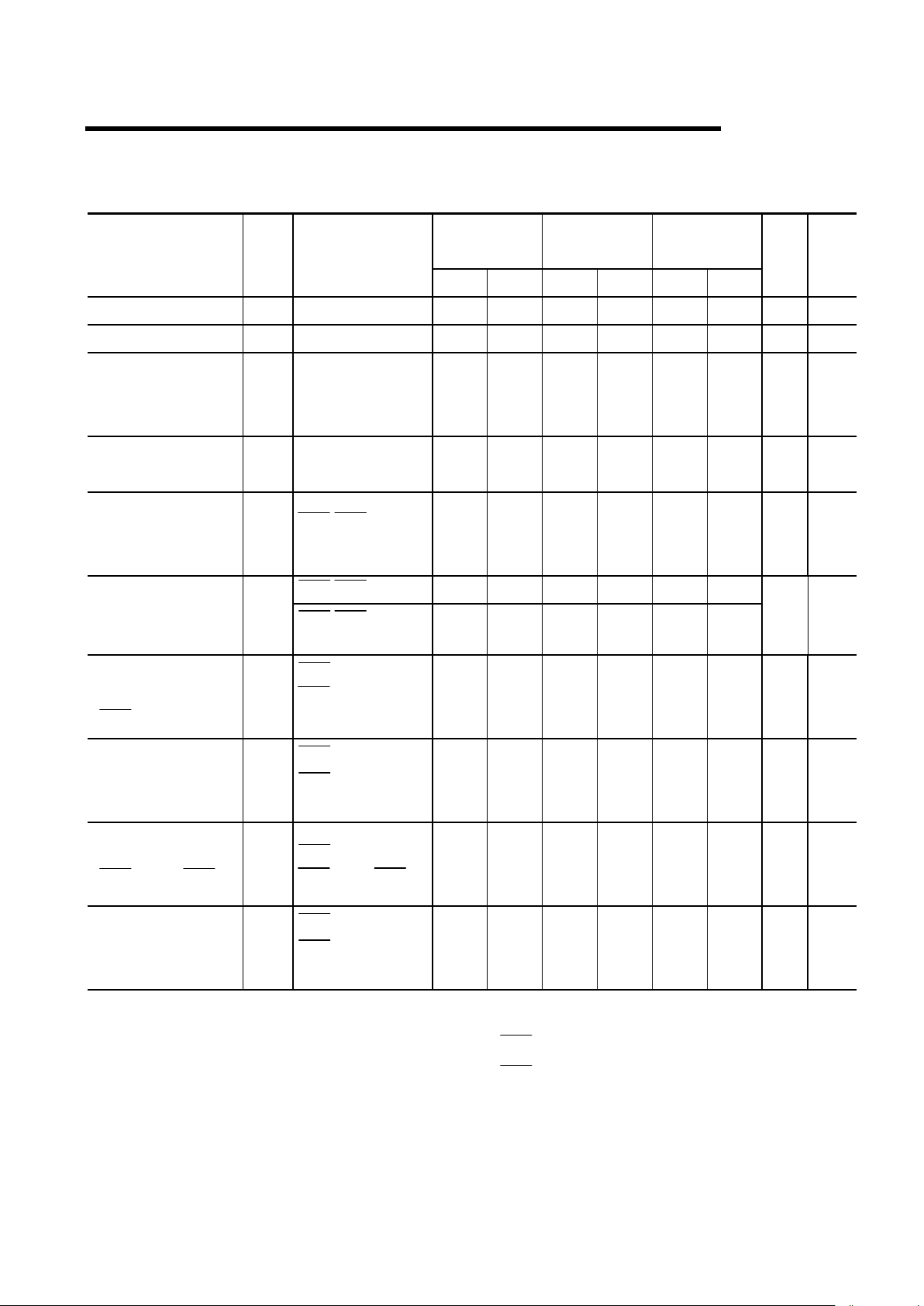
AC Characteristic (1/2)
(VCC = 5V ± 10%, Ta = 0°C to 70°C) Note1, 2, 3, 11, 12
MSM5117800
D-50
MSM5117800
D-60
MSM5117800
D-70
Parameter Symbol
Min. Max. Min. Max. Min. Max.
Unit Note
Random Read or Write Cycle Time
t
RC
90
¾
110
¾
130
¾
ns
Read Modify Write Cycle Time
t
RWC
131
¾
155
¾
185
¾
ns
Fast Page Mode Cycle Time
t
PC
35
¾
40
¾
45
¾
ns
Fast Page Mode Read Modify
Write Cycle Time
t
PRWC
76
¾
85
¾
100
¾
ns
Access Time from RAS
t
RAC
¾
50
¾
60
¾
70 ns 4,5,6
Access Time from CAS
t
CAC
¾
13
¾
15
¾
20 ns 4,5
Access Time from Column Address
t
AA
¾
25
¾
30
¾
35 ns 4,6
Access Time from CAS Precharge
t
CPA
¾
30
¾
35
¾
40 ns 4
Access Time from OE
t
OEA
¾
13
¾
15
¾
20 ns 4
Output Low Impedance Time from
CAS
t
CLZ
0
¾
0
¾
0
¾
ns 4
CAS to Data Output Buffer Turnoff Delay Time
t
OFF
013015020ns7
OE to Data Output Buffer Turn-off
Delay Time
t
OEZ
013015020ns7
Transition Time
t
T
350350350ns3
Refresh Period
t
REF
¾
32
¾
32
¾
32
m
RAS Precharge Time
t
RP
30
¾
40
¾
50
¾
ns
RAS Pulse Width
t
RAS
50 10,000 60 10,000 70 10,000 ns
RAS Pulse Width (Fast Page Mode)
t
RASP
50 100,000 60 100,000 70 100,000 ns
RAS Hold Time
t
RSH
13
¾
15
¾
20
¾
ns
RAS Hold Time referenced to OE
t
ROH
13
¾
15
¾
20
¾
ns
CAS Precharge Time
(Fast Page Mode)
t
CP
7
¾
10
¾
10
¾
ns
CAS Pulse Width
t
CAS
13 10,000 15 10,000 20 10,000 ns
CAS Hold Time
t
CSH
50
¾
60
¾
70
¾
ns
CAS to RAS Precharge Time
t
CRP
5
¾
5
¾
5
¾
ns
RAS Hold Time from CAS Precharge
t
RHCP
30
¾
35
¾
40
¾
ns
RAS to CAS Delay Time
t
RCD
17 37 20 45 20 50 ns 5
RAS to Column Address Delay Time
t
RAD
12 25 15 30 15 35 ns 6
Row Address Set-up Time
t
ASR
0
¾
0
¾
0
¾
ns
Row Address Hold Time
t
RAH
7
¾
10
¾
10
¾
ns
Column Address Set-up Time
t
ASC
0
¾
0
¾
0
¾
ns
Page 7

MSM5117800D
7/14
AC Characteristic (2/2)
(VCC = 5V ± 10%, Ta = 0°C to 70°C) Note1, 2, 3, 11, 12
MSM5117800
D-50
MSM5117800
D-60
MSM5117800
D-70
Parameter
Symbol
Min. Max. Min. Max. Min. Max.
Unit Note
Column Address Hold Time
t
CAH
7
¾
15
¾
15
¾
ns
Column Address to RAS Lead Time
t
RAL
25
¾
30
¾
35
¾
ns
Read Command Set-up Time
t
RCS
0
¾
0
¾
0
¾
ns
Read Command Hold Time
t
RCH
0
¾
0
¾
0
¾
ns 8
Read Command Hold Time
referenced to RAS
t
RRH
0
¾
0
¾
0
¾
ns 8
Write Command Set-up Time
t
WCS
0
¾
0
¾
0
¾
ns 9
Write Command Hold Time
t
WCH
7
¾
10
¾
15
¾
ns
Write Command Pulse Width
t
WP
7
¾
10
¾
10
¾
ns
OE Command Hold Time
t
OEH
13
¾
15
¾
20
¾
ns
Write Command to RAS Lead Time
t
RWL
13
¾
15
¾
20
¾
ns
Write Command to CAS Lead Time
t
CWL
13
¾
15
¾
20
¾
ns
Data-in Set-up Time
t
DS
0
¾
0
¾
0
¾
ns 10
Data-in Hold Time
t
DH
7
¾
15
¾
15
¾
ns 10
OE to Data-in Delay Time
t
OED
13
¾
15
¾
20
¾
ns
CAS to WE Delay Time
t
CWD
36
¾
40
¾
50
¾
ns 9
Column Address to WE Delay Time
t
AWD
48
¾
55
¾
65
¾
ns 9
RAS to WE Delay Time
t
RWD
73
¾
85
¾
100
¾
ns 9
CAS Precharge WE Delay Time
t
CPWD
53
¾
60
¾
70
¾
ns 9
CAS Active Delay Time from RAS
Precharge
t
RPC
10
¾
10
¾
10
¾
ns
RAS to CAS Set-up Time
(CAS before RAS)
t
CSR
10
¾
10
¾
5
¾
ns
RAS to CAS Hold Time
(CAS before RAS)
t
CHR
10
¾
10
¾
10
¾
ns
WE to RAS Precharge Time
(CAS before RAS)
t
WRP
10
¾
10
¾
10
¾
ns
WE Hold Time from RAS
(CAS before RAS)
t
WRH
10
¾
10
¾
10
¾
ns
RAS to WE Set-up Time (Test Mode)
t
WTS
10
¾
10
¾
10
¾
ns
RAS to WE Hold Time (Test Mode)
t
WTH
10
¾
10
¾
10
¾
ns
Page 8

MSM5117800D
8/14
Notes: 1. A start-up delay of 200ms is required after power-up, followed by a minimum of eig ht initialization
cycles (RAS-only refresh or CAS before RAS refresh) before proper device operation is achieved.
2. The AC characteristics assume t
T
= 5ns.
3. V
IH
(Min.) and VIL (Max.) are reference levels for measuring input timing signals. Transition times
(t
T
) are measured between VIH and VIL.
4. This parameter is measured with a load circuit equivalent to 2 TTL load and 100pF.
5. Operation within the t
RCD
(Max.) limit ensures that t
RAC
(Max.) can be met.
t
RCD
(Max.) is specified as a reference point only. If t
RCD
is greater than the specified t
RCD
(Max.)
limit, then the access time is controlled by t
CAC
.
6. Operation within the t
RAD
(Max.) limit ensures that t
RAC
(Max.) can be met.
t
RAD
(Max.) is specified as a reference point only. If t
RAD
is greater than the specified t
RAD
(Max.)
limit, then the access time is controlled by t
AA
.
7. t
OFF
(Max.) and t
OEZ
(Max.) define the time at which the output achieved the open circuit
condition and are not referenced to output voltage levels.
8. t
RCH
or t
RRH
must be satisfied for a read cycle.
9. t
WCS
, t
CWD
, t
RWD
, t
AWD
and t
CPWD
are not restrictive operating parameters. They are included in
the data sheet as electrical characteristics only. If t
WCS
³ t
WCS
(Min.), then the cycle is an early
write cycle and the data out will remain open circuit (high impedance) throughout the entire cycle.
If t
CWD
³ t
CWD
(Min.), t
RWD
³ t
RWD
(Min.), t
AWD
³
t
AWD
(Min.) and t
CPWD
³ t
CPWD
(Min.), then
the cycle is a read modify write cycle and data out will contain data read from the selected cell; if
neither of the above sets of conditions is satisfied, then the condition of the data out (at access time)
is indeterminate.
10. These parameters are referenced to the CAS leading edge in an early write cycle, and to the WE
leading edge in an OE control write cycle, or a read modify write cycle.
11. The test mode is initiated by performing a WE and CAS before RAS refresh cycle. This mode is
latched and remains in effect until the exit cycle is generated. The test mode specified in this data
sheets is a 2-bit parallel test function, CA0 and CA1 are not used. I n a read cy cle, if all internal bits
are equal, the DQ pin will indicate a high level. If any internal bits are not equal, the DQ pin will
indicate a low level. The test mode is cleared and the memory device returned to its normal
operating state by performing a RAS-only refresh cycle or a CAS before RAS refresh cycle.
12. In a test mode read cycle, the value of access time parameters is delayed for 5ns for the specified
value. These parameters should be specified in test mode cycle by adding the above value to the
specified value in this data sheet.
Page 9

MSM5117800D
9/14
Timing Chart
· Read Cycle
· Write Cycle (Early Write)
t
WCS
t
WCH
t
CWL
t
ASR
t
RAH
t
ASC
t
CRP
t
RP
t
RC
t
RAS
Valid Data-in
t
DH
t
RWL
Row
t
CSH
t
CRP
t
RCD
t
RSH
t
CAS
Column
t
CAH
t
RAD
t
RAL
t
DS
t
WP
RAS
V
IH
V
IL
CAS
V
IH
V
IL
Address
V
IH
V
IL
WE
V
IH
V
IL
OE
V
IH
V
IL
DQ
V
IH
V
IL
“H” or “L”
Open
t
OFF
t
CLZ
t
CAC
t
OEA
t
ASC
t
RRH
t
RAH
t
ASR
t
RAD
t
RAL
t
CRP
t
CAH
t
CRP
t
RCD
t
RC
Row
t
RAS
t
RP
t
CSH
t
RSH
t
CAS
Column
t
RAC
t
AA
t
RCS
t
ROH
Valid Data-out
t
RCH
t
OEZ
Open
RAS
V
IH
V
IL
CAS
V
IH
V
IL
Address
V
IH
V
IL
WE
V
IH
V
IL
OE
V
IH
V
IL
DQ
V
OH
V
OL
“H” or “L”
Page 10

MSM5117800D
10/14
· Read Modify Write Cycle
t
DH
t
DS
t
OEZ
t
CLZ
t
OED
t
AA
t
OEH
t
RWD
t
CWD
t
CWL
t
RWL
t
CAH
t
ASC
t
ASR
t
RAH
t
RAD
t
CRP
t
RCD
t
RSH
t
CAS
t
CRP
t
CAC
Valid
Data-out
Row
t
CSH
Column
t
RAC
t
OEA
t
RCS
t
AWD
t
WP
t
RWC
t
RAS
t
RP
RAS
V
IH
V
IL
CAS
V
IH
V
IL
Address
V
IH
V
IL
WE
V
IH
V
IL
OE
V
IH
V
IL
DQ
V
I/OH
V
I/OL
“H” or “L”
Valid
Data-in
Page 11

MSM5117800D
11/14
· Fast Page Mode Cycle
· Fast Page Mode Write Cycle (Early Write)
t
WP
t
RWL
t
WCH
t
CWL
t
WP
t
CWL
t
WCH
t
WP
t
WCH
t
CSH
t
RAL
t
CRP
t
DH
t
DS
t
DH
t
DS
t
DH
t
DS
Valid *
Data-in
t
WCS
t
WCS
t
WCS
t
ASC
t
CAH
t
ASC
t
CAH
t
RAD
t
ASR
t
ASC
t
RAH
t
RCD
t
CRP
t
CAS
t
CAS
t
RSH
t
CP
t
CAS
t
RP
t
RHPC
Valid *
Data-in
Valid *
Data-in
“H” or “L”
t
CAH
t
CP
t
PC
RAS
V
IH
V
IL
CAS
V
IH
V
IL
Address
V
IH
V
IL
WE
V
IH
V
IL
DQ
V
IH
V
IL
t
RASP
Row Column Column Column
t
CWL
Note: OE = “H” or “L”
t
PC
t
CAS
t
OEZ
t
CAC
t
OFF
t
CAC
t
CLZ
t
OEA
t
CSH
t
CAC
t
OEZ
t
RRH
t
RAC
t
OEA
t
RAL
t
ASC
t
CAH
t
RCS
t
RCH
t
CPA
t
AA
t
AA
t
RCH
t
RCS
t
CAH
t
ASC
t
RAH
t
RAD
t
RCS
t
ASR
t
ASC
t
CP
t
CAS
t
RSH
t
RASP
t
CAS
t
CP
t
RCD
t
CRP
t
CLZ
t
CAH
Valid
Data-out
t
CPA
t
RP
RAS
V
IH
V
IL
CAS
V
IH
V
IL
Address
V
IH
V
IL
WE
V
IH
V
IL
OE
V
IH
V
IL
DQ
V
OH
V
OL
t
RHCP
Row Column Column Column
“H” or “L”
t
CRP
t
RCH
t
AA
t
OEA
t
OFF
t
OEZ
Valid
Data-out
t
CLZ
t
OFF
Valid
Data-out
Page 12

MSM5117800D
12/14
· Fast Page Mode Read Modify Write Cycle
· RAS-only Refresh Cy cle
t
ASRtRAH
t
CRP
t
RPC
t
RP
t
RAS
t
RC
t
OFF
RAS
V
IH
V
IL
CAS
V
IH
V
IL
V
IH
V
IL
Address
V
OH
V
OL
DQ
“H” or “L”
Row
Open
Note: WE, OE = “H” or
Row
Column
t
AA
t
DH
t
DS
t
ROH
t
CPWD
t
RWL
t
CWL
t
RCS
Column
t
WP
t
CPWD
t
CWD
t
CWL
t
CWD
t
AWD
t
RAL
t
CAH
t
CRP
t
CP
t
CAS
t
CLZ
t
CAS
t
ASC
t
ASC
t
OED
t
DH
t
OEZ
t
OED
t
CAC
t
OED
t
DH
t
OEZ
t
OEA
t
AWD
In
t
WP
t
DS
t
AA
t
DS
Column
t
RP
t
RAH
t
RSH
t
ASR
t
RAD
t
CAH
Out
t
CSH
t
CAS
t
RAC
t
RASP
t
OEZ
t
RCS
t
CAC
t
PRWC
t
RCS
t
CAC
t
CLZ
t
CLZ
t
WP
t
CWL
t
AWD
t
RCD
t
CPA
t
CP
t
OEA
t
AA
t
CPA
t
OEA
t
PWD
t
CWD
t
CAH
t
ASC
In InOu Ou
RAS
V
IH
V
IL
CAS
V
IH
V
IL
Address
V
IH
V
IL
WE
V
IH
V
IL
OE
V
IH
V
IL
DQ
V
I/OH
V
I/OL
“H” or “L”
Page 13

MSM5117800D
13/14
· CAS befor e RAS Ref r es h Cycle
· Hidden Refresh Read Cycle
RAS
t
OFF
t
RPC
t
RP
t
RC
t
RAS
t
CHR
t
CSR
t
RP
t
CP
t
RPC
V
IH
V
IL
CAS
V
IH
V
IL
V
OH
V
OL
DQ
Open
Note: WE, OE, Address = “H” or “H” or “L”
t
OFF
t
RAC
t
CLZ
t
OEZ
t
ROH
t
OEA
t
CAC
t
RRH
t
AA
t
RAL
t
RCS
t
CAH
t
RAH
t
ASR
t
ASC
Column
t
RAD
t
RP
t
RAS
t
RC
t
RP
t
CHR
t
RAS
t
RSH
t
RCD
t
CRP
t
RC
RAS
V
IH
V
IL
CAS
V
IH
V
IL
Address
V
IH
V
IL
WE
V
IH
V
IL
OE
V
IH
V
IL
DQ
V
OH
V
OL
Open
Row
Valid Data-out
“H” or “L”
Page 14

MSM5117800D
14/14
Hidden Refresh Write Cycle
t
DS
t
DH
t
WCH
t
RAL
t
WP
t
WCS
t
CAH
t
RAH
t
ASR
t
ASC
Column
t
RAD
t
RP
t
RAS
t
RC
t
RP
t
CHR
t
RAS
t
RSH
t
RCD
t
CRP
t
RC
RAS
V
IH
V
IL
CAS
V
IH
V
IL
Address
V
IH
V
IL
WE
V
IH
V
IL
OE
V
IH
V
IL
DQ
V
IH
V
IL
Row
Valid Data-in
“H” or “L”
 Loading...