

Datasheet MSM5116400D-60TS-K, MSM5116400D-50TS-K, MSM5116400D-70SJ, MSM5116400D-60SJ, MSM5116400D-70TS-K Datasheet (OKI)
...Page 1

Semiconductor
M SM5116400D
This version:Apr.1999
4,194,304-Word
4-Bit DYNA MIC RAM : FAST PAGE MODE TY PE
´´´´
DESCRIPTION
The MSM5116400D is a 4,194,304-word ´ 4-bit dynamic RAM fabricated in Oki’s silicon-gate CMOS
technology. The MSM5116400D achieves high integration, high-speed operation, and low-power consumption
because Oki manufactures the device in a quadruple-layer polysilicon/double-layer metal CMOS process. The
MSM5116400D is available in a 26/24-pin plastic SOJ, 26/24-pin plastic TSOP.
FEATURES
4,194,304-word ´ 4-bit configuration
·
Single 5V power supply, ±10% tolerance
·
Input : TTL compatible, low input capacitance
·
· Output : TTL compatible, 3-state
· Refresh : 4096 cycles/64 ms
· Fast page mode, read modify write capability
CAS before RAS refresh, hidden refresh, RAS-only refresh capability
·
· Multi-bit test mode capability
· Package options:
26/24-pin 300mil plastic SOJ (SOJ26/24-P-300-1.27) (Product : MSM5116400D-xxSJ)
26/24-pin 300mil plastic TSOP (TSOPII26/24-P-300-1.27-K) (Product : MSM5116400D-xxTS-K)
xx : indicates speed rank.
PRODUCT FAMILY
Family
MSM5116400D-50 50ns 25ns 13ns 13ns 90ns 413mW
MSM5116400D-60 60ns 30ns 15ns 15ns 110ns 385mW
MSM5116400D-70 70ns 35ns 20ns 20ns 130ns 358mW
Access Time (Max.) Power Dissipation
t
RAC
t
AA
t
CAC
t
OEA
Cycle Time
(Min.)
Operating (Max.) Standby (Max.)
5.5mW
1/14
Page 2
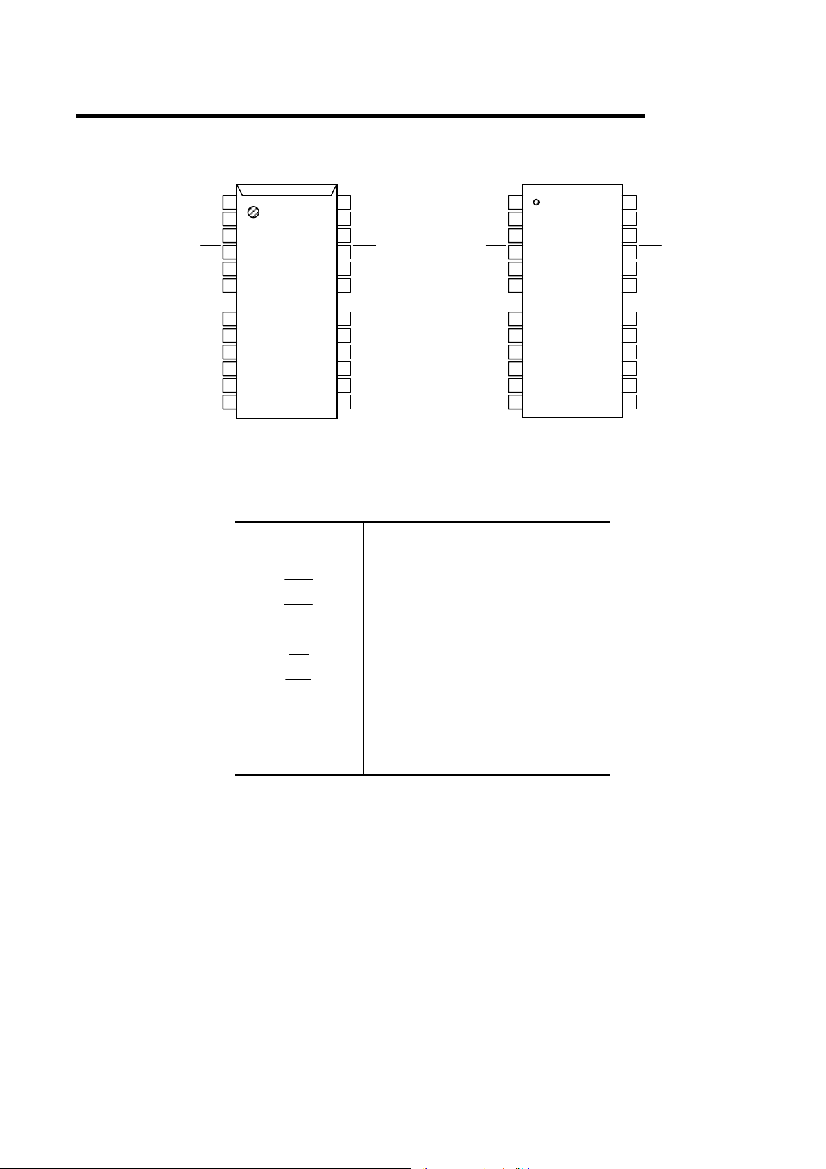
PIN CONFIGRATION (TOP VIEW)
MSM5116400D
V
1
CC
DQ1
2
DQ2
3
WE
4
RAS
5
A11
6
A10
8
9
A0
10
A1
11
A2
12
A3
13
V
CC
26/24-Pin Plastic SOJ
Pin Name Function
A0–A11 Address Input
V
DQ1
DQ2
WE
RAS
A11
A10
A0
A1
A2
A3
V
1
CC
2
3
4
5
6
8
9
10
11
12
13
CC
26
25
24
23
22
21
19
18
17
16
15
14
V
SS
DQ4
DQ3
CAS
OE
A9
A8
A7
A6
A5
A4
V
SS
26/24-Pin Plastic TSOP
RAS Row Address Strobe
(K Type)
26
25
24
23
22
21
19
18
17
16
15
14
V
SS
DQ4
DQ3
CAS
OE
A9
A8
A7
A6
A5
A4
V
SS
CAS Column Address Strobe
DQ1–DQ4 Data Input/Data Output
OE Output Enable
WE Write Enable
V
CC
V
SS
Power Supply (5V)
Ground (0V)
NC No Connection
2/14
Page 3
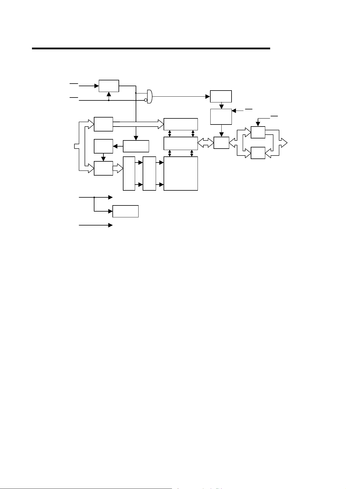
BLOCK DIAGRAM
A
DQ
DQ
OE
WE
RAS
CAS
VCCV
Column
10
Address
Buffers
Internal
0 – A11
Address
Counter
Address
Buffers
Timing
Generator
Row
1212
On Chip
V
Generator
BB
Refresh
Control Clock
Row
Deco-
ders
Word
Drivers
10
Column Decoders
Sense Amplifiers
Memory
Cells
Timing
Generator
Write
Clock
Generator
I/O
Selector
MSM5116400D
Output
4
Buffers
44
4
Buffers
Input
4
4
4
1 -
4
SS
3/14
Page 4
ELECTRICAL CHARACTERISTICS
Absolute Maximum Ratings
Parameter Symbol Rating Unit
MSM5116400D
Voltage on Any Pin Relative to V
SS
Short Circuit Output Current
Power Dissipation
Operating Temperature
Storage Temperature
*: Ta = 25°C
Recommended Operating Conditions
Parameter Symbol Min. Typ. Max. Unit
V
Power Supply Voltage
Input High Voltage
Input Low Voltage
V
V
V
CC
SS
IH
IL
V
T
I
OS
P
D*
T
opr
T
stg
0.5 to 7.0
-
50 mA
1W
0 to 70 °C
55 to 150
-
V
°C
(Ta = 0°C to 70°C)
4.5 5.0 5.5 V
000V
*1
0.5
+
0.8 V
V
-
2.4
0.5
¾
*2
¾
V
CC
Notes: *1. The input voltage is VCC + 2.0V when the pulse width is less than 20ns (the pulse width is with
respect to the point at which V
*2. The input voltage is V
the point at which V
SS
- 2.0V when the pulse width is less than 20ns (the pulse width respect to
SS
is applied).
is applied).
CC
Capacitance
(VCC = 5.0V ± 10%, Ta = 25°C, f=1MHz)
Parameter Symbol Typ. Max. Unit
Input Capacitance (A0 – A11)
Input Capacitance
(RAS, CAS, WE, OE)
Output Capacitance (DQ1 – DQ4)
C
C
C
IN1
IN2
I/O
¾
¾
¾
5pF
7pF
7pF
4/14
Page 5
DC Characteristics
MSM5116400D
(VCC = 5V ± 10%, Ta = 0°C to 70°C)
Parameter
Output High Voltage
Output Low Voltage
Input Leakage
Current
Output Leakage
Current
Average Power
Supply Current
(Operating)
Power Supply
Current
(Standby)
Average Power
Supply Current
(RAS-only Refresh)
Symbol
V
OH
V
OLIOL
I
LI
I
LO
I
CC1
I
CC2
I
CC3
Condition
IOH = -5.0mA
= 4.2mA
0V £ VI £ 6.5V ;
All other pins not
under test = 0V
DQ disable
0V £ V
O
£ V
CC
RAS, CAS cycling,
t
= Min.
RC
RAS, CAS = V
RAS, CAS
– 0.2V
V
CC
IH
³
RAS cycling,
CAS = V
t
RC
= Min.
IH
,
MSM5116400
D-50
Min.
Max
2.4 V
MSM5116400
Min.
2.4 V
CC
D-60
Max
CC
MSM5116400
D-70
Min.
2.4 V
Max
CC
Unit Note
V
00.400.400.4V
10
-
10
-
¾
¾
10
10
75
2
10
-
10
-
¾
¾
10
10
70
2
10
-
10
-
¾
¾
10
10
A
m
A
m
65 mA 1,2
2
mA 1
¾
¾
0.5
75
¾
¾
0.5
70
¾
¾
0.5
65 mA 1,2
I
CC5
RAS = VIH,
CAS = V
,
IL
DQ = enable
¾
2
Power Supply
Current
(Standby)
Average Power
Supply Current
(CAS before RAS
RAS = cycling,
I
CC6
CAS before RAS
¾
75
Refresh)
I
CC7
RAS = VIL,
CAS cycling,
t
= Min.
PC
¾
70
Average Power
Supply Current
(Fast Page Mode)
Notes: 1. ICC Max. is specified as ICC for output open condition.
2. The address can be changed once or less while RAS = V
3. The address can be changed once or less while CAS = V
¾
¾
¾
2
70
65
.
IL
.
IH
¾
¾
¾
2mA1
65 mA 1,2
60 mA 1,3
5/14
Page 6

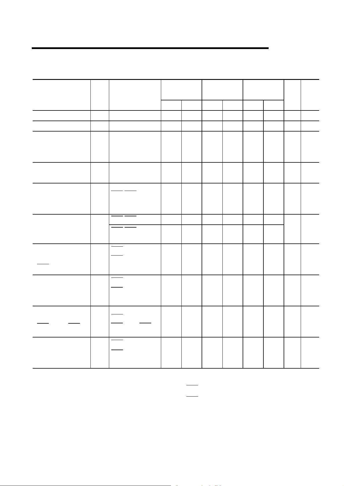
AC Characteristic (1/2)
MSM5116400D
(VCC = 5V ± 10%, Ta = 0°C to 70°C) Note1,2,3
Parameter Symbol
Random Read or Write Cycle Time
Read Modify Write Cycle Time
Fast Page Mode Cycle Time
Fast Page Mode Read Modify
Write Cycle Time
Access Time from RAS
Access Time from CAS
Access Time from Column Address
Access Time from CAS Precharge
Access Time from OE
Output Low Impedance Time from
CAS
CAS to Data Output Buffer Turn-
off Delay Time
OE to Data Output Buffer Turn-off
Delay Time
t
RC
t
RWC
t
PC
t
PRWC
t
RAC
t
CAC
t
AA
t
CPA
t
OEA
t
CLZ
t
OFF
t
OEZ
MSM5116400
D-50
MSM5116400
D-60
MSM5116400
D-70
Unit Note
Min. Max. Min. Max. Min. Max.
90
131
35
76
¾
¾
¾
¾
¾
0
¾
¾
¾
¾
50
13
25
30
13
¾
110
155
40
85
¾
¾
¾
¾
¾
0
¾
¾
¾
¾
60
15
30
35
15
¾
130
185
45
100
¾
¾
¾
¾
¾
0
¾
¾
¾
¾
ns
ns
ns
ns
70 ns 4,5,6
20 ns 4,5
35 ns 4,6
40 ns 4
20 ns 4
¾
ns 4
013015020ns7
013015020ns7
Transition Time
Refresh Period
RAS Precharge Time
RAS Pulse Width
RAS Pulse Width (Fast Page Mode)
RAS Hold Time
RAS Hold Time referenced to OE
CAS Precharge Time
(Fast Page Mode)
CAS Pulse Width
CAS Hold Time
CAS to RAS Precharge Time
RAS Hold Time from CAS Precharge
RAS to CAS Delay Time
RAS to Column Address Delay Time
Row Address Set-up Time
Row Address Hold Time
Column Address Set-up Time
t
t
REF
t
RP
t
RAS
t
RASP
t
RSH
t
ROH
t
CP
t
CAS
t
CSH
t
CRP
t
RHCP
t
RCD
t
RAD
t
ASR
t
RAH
t
ASC
T
350350350ns3
¾
30
64
¾
¾
40
64
¾
¾
50
64
¾
m
ns
50 10,000 60 10,000 70 10,000 ns
50 100,000 60 100,000 70 100,000 ns
13
13
¾
¾
7
¾
15
15
10
¾
¾
¾
20
20
10
¾
¾
¾
ns
ns
ns
13 10,000 15 10,000 20 10,000 ns
50
30
¾
5
¾
¾
60
5
35
¾
¾
¾
70
5
40
¾
¾
¾
ns
ns
ns
17 37 20 45 20 50 ns 5
12 25 15 30 15 35 ns
0
7
0
¾
¾
¾
0
10
0
¾
¾
¾
0
10
0
¾
¾
¾
ns
ns
ns
6/14
Page 7

AC Characteristic (2/2)
MSM5116400D
(VCC = 5V ± 10%, Ta = 0°C to 70°C) Note1,2,3
Parameter
Column Address Hold Time
Column Address to RAS Lead Time
Read Command Set-up Time
Read Command Hold Time
Read Command Hold Time
referenced to RAS
Write Command Set-up Time
Write Command Hold Time
Write Command Pulse Width
OE Command Hold Time
Write Command to RAS Lead Time
Write Command to CAS Lead Time
Data-in Set-up Time
Data-in Hold Time
OE to Data-in Delay Time
CAS to WE Delay Time
Column Address to WE Delay Time
RAS to WE Delay Time
CAS Precharge WE Delay Time
Symbol
t
CAH
t
RAL
t
RCS
t
RCH
t
RRH
t
WCS
t
WCH
t
WP
t
OEH
t
RWL
t
CWL
t
DS
t
DH
t
OED
t
CWD
t
AWD
t
RWD
t
CPWD
MSM5116400
D-50
MSM5116400
D-60
MSM5116400
D-70
Min. Max. Min. Max. Min. Max.
25
13
13
13
13
36
48
73
53
7
¾
¾
0
0
0
0
7
7
¾
¾
¾
¾
¾
¾
¾
¾
¾
0
7
¾
¾
¾
¾
¾
¾
¾
15
30
0
0
0
0
10
10
15
15
15
0
10
15
40
55
85
60
¾
¾
¾
¾
¾
¾
¾
¾
¾
¾
¾
¾
¾
¾
¾
¾
¾
¾
15
35
0
0
0
0
15
10
20
20
20
0
15
20
50
65
100
70
¾
¾
¾
¾
¾
¾
¾
¾
¾
¾
¾
¾
¾
¾
¾
¾
¾
¾
Unit Note
ns
ns
ns
ns 8
ns 8
ns 9
ns
ns
ns
ns
ns
ns 10
ns 10
ns
ns 9
ns 9
ns 9
ns 9
CAS Active Delay Time from RAS
Precharge
RAS to CAS Set-up Time
(CAS before RAS)
RAS to CAS Hold Time
(CAS before RAS)
t
RPC
t
CSR
t
CHR
10
10
5
¾
¾
¾
5
10
10
¾
¾
¾
5
10
10
¾
¾
¾
ns
ns
ns
7/14
Page 8

MSM5116400D
Notes: 1. A start-up delay of 200ms is required after power-up, followed by a minimum of eig ht initialization
cycles (RAS-only refresh or CAS before RAS refresh) before proper device operation is achieved.
2. The AC characteristics assume t
3. V
(Min.) and VIL (Max.) are reference levels for measuring input tim ing signals. Transition tim es
IH
(t
) are measured between VIH and VIL.
T
= 5ns.
T
4. This parameter is measured with a load circuit equivalent to 2 TTL load and 100pF.
5. Operation within the t
t
(Max.) is specified as a reference point only. If t
RCD
limit, then the access time is controlled by t
6. Operation within the t
t
(Max.) is specified as a reference point only. If t
RAD
limit, then the access time is controlled by t
7. t
(Max.) and t
OFF
OEZ
(Max.) limit ensures that t
RCD
CAC
(Max.) limit ensures that t
RAD
AA
.
.
(Max.) can be met.
RAC
is greater than the specified t
RCD
(Max.) can be met.
RAC
is greater than the specified t
RAD
RCD
RAD
(Max.) define the time at which the output achieved the open circuit condition
and are not referenced to output voltage levels.
8. t
9. t
RCH
WCS
or t
, t
must be satisfied for a read cycle.
RRH
, t
, t
CWD
RWD
AWD
and t
are not restrictive operating parameters. They are included in the
CPWD
data sheet as electrical characteristics only. If t
WCS
³ t
(Min.), then the cycle is an early write
WCS
cycle and the data out will rem ain open circuit (high im pedance) throughout the entire cycle. If t
³
t
CWD
(Min.), t
RWD
³ t
RWD
(Min.), t
AWD
(Min.) and t
t
³
AWD
CPWD
³ t
(Min.), then the cycle is a
CPWD
read modify write cycle and data out will contain data read from the selected cell; if neither of the
above sets of conditions is satisfied, then the condition of the data out (at access time) is
indeterminate.
(Max.)
(Max.)
CWD
10. These parameters are referenced to the CAS leading edge in an early write cycle, and to the WE
leading edge in an OE control write cycle, or a read modify write cycle.
8/14
Page 9

Timing Chart
MSM5116400D
· Read Cycle
V
RAS
CAS
IH
V
V
IH
V
V
Address
IH
V
V
OE
IH
V
V
IH
WE
V
V
OH
DQ
V
OL
t
RC
t
RAS
t
t
t
RRH
RCH
RP
t
CRP
t
OFF
IL
t
CRP
IL
t
t
ASR
Row
IL
IL
IL
RAH
t
RAD
t
RCD
t
t
ASC
RCS
t
RAC
Column
Open
t
CLZ
t
CSH
t
t
AA
CAH
t
t
CAC
OEA
t
RAL
t
RSH
t
CAS
t
ROH
t
OEZ
Valid Data-out
“H” or “L”
· Write Cycle (Early Write)
V
OE
DQ
IH
V
IL
t
CRP
V
IH
V
IL
t
ASR
V
IH
V
IL
V
IH
V
IL
V
IH
V
IL
V
IH
V
IL
RAS
CAS
Address
WE
Row
t
RAH
t
RAD
t
RCD
t
ASC
t
WCS
t
WP
t
DS
Valid Data-in
Column
t
t
CSH
CAH
t
RAS
t
WCH
t
DH
t
RC
t
RP
t
CRP
t
CWL
t
RAL
t
RSH
t
CAS
t
RWL
Open
“H” or “L”
9/14
Page 10

· Read Modify Write Cycle
V
OE
DQ
IH
V
IL
t
CRP
V
IH
V
IL
t
ASR
V
IH
V
IL
V
IH
V
IL
V
IH
V
IL
V
I/OH
V
I/OL
RAS
CAS
Address
WE
Row
t
RAH
t
RAD
t
RCD
t
t
ASC
RCS
t
RAC
Column
t
AA
t
CLZ
t
t
CSH
CAC
t
RAS
t
t
RWD
CAH
t
RWC
t
RSH
t
CAS
t
CWD
t
OEA
Valid
Data-out
t
AWD
t
OED
t
OEZ
t
t
t
DS
Valid
Data-in
t
WP
OEH
CWL
t
RWL
t
DH
MSM5116400D
t
RP
t
CRP
“H” or “L”
10/14
Page 11

· Fast Page Mode Cycle
V
RAS
CAS
Address
WE
OE
DQ
IH
V
IL
t
CRP
V
IH
V
IL
t
ASR
V
IH
V
IL
V
IH
V
IL
V
IH
V
IL
V
OH
V
OL
t
RASP
t
RAD
t
t
CSH
t
RAH
RCD
t
ASC
t
CAH
t
CAS
t
PC
t
CP
t
ASC
t
CAH
t
CAS
t
ASC
t
RHCP
t
CP
Row Column Column Column
t
CPA
t
RCS
t
AA
t
t
CLZ
t
OEA
CAC
t
RCH
t
Valid
Data-out
OFF
t
CPA
t
t
AA
OEZ
t
RCS
t
t
RCS
t
RAC
t
t
AA
CLZ
t
t
OEA
CAC
t
RCH
t
t
Valid
Data-out
OFF
OEZ
MSM5116400D
t
RSH
t
CAS
t
RAL
t
CAH
t
OEA
t
CAC
CLZ
t
OEZ
Valid
Data-out
t
RP
t
CRP
t
RCH
t
RRH
t
OFF
· Fast Page Mode Write Cycle (Early Write)
V
RAS
CAS
Address
WE
DQ
IH
V
IL
V
IH
V
IL
V
IH
V
IL
V
IH
V
IL
V
IH
V
IL
t
t
CRP
ASR
t
RAD
t
t
RCD
RAH
t
ASC
Row Column Column Column
t
WCS
t
DS
Valid *
Data-in
t
t
t
WCH
t
t
CSH
CAH
t
CWL
WP
CAS
t
DH
t
WCS
t
RASP
t
t
DS
CP
t
ASC
t
PC
t
CAS
t
CAH
t
CWL
t
WCH
t
WP
t
DH
Valid *
Data-in
Note: OE = “H” or “L”
t
t
ASC
t
WCS
t
DS
CP
t
RHPC
t
t
Valid *
Data-in
t
t
CAH
t
CWL
WP
t
CAS
RAL
RWL
t
t
RSH
DH
t
WCH
“H” or “L”
t
RP
t
CRP
“H” or “L”
11/14
Page 12

· Fast Page Mode Read Modify Write Cycle
t
AA
CSH
Column
t
PWD
t
t
AWD
CAH
t
CWD
t
t
CAS
t
DS
RAS
CAS
Address
WE
V
IH
V
IL
V
IH
V
IL
t
RAH
t
ASR
V
IH
V
IL
V
IH
V
IL
Row
t
t
t
t
RAD
t
RCS
RAC
RCD
ASC
t
t
V
OE
DQ
IH
V
IL
V
I/OH
V
I/OL
t
CLZ
t
CAC
t
Out
CWL
t
t
OEA
OED
WP
DH
t
OEZ
In
t
t
t
CP
CAC
CLZ
t
RASP
t
ASC
Column
t
RCS
t
CPA
t
AA
t
CWD
t
t
t
AWD
t
OEA
t
PRWC
t
CAS
CAH
t
CWL
CPWD
t
WP
t
DS
t
DH
t
OED
t
OEZ
In InOu Ou
t
t
t
AA
t
CAC
CLZ
CP
t
ASC
Column
t
RCS
t
t
t
CWD
AWD
t
t
CAS
t
CAH
CPWD
t
ROH
CPA
t
OEA
MSM5116400D
t
RSH
t
RAL
t
CWL
t
WP
t
DH
t
DS
t
OED
t
OEZ
t
CRP
t
RWL
“H” or “L”
t
RP
· RAS-only Refresh Cy cle
V
RAS
CAS
Address
DQ
IH
V
IL
V
IH
V
IL
V
IH
V
IL
V
OH
V
OL
t
CRP
t
ASRtRAH
Row
t
OFF
t
RAS
t
RC
t
RP
t
RPC
Open
Note: WE, OE = “H” or
“H” or “L”
12/14
Page 13

· CAS befor e RAS Ref r es h Cycle
t
RP
V
RAS
CAS
IH
V
IL
V
IH
V
IL
t
RPC
t
CP
t
V
OH
DQ
V
OL
· Hidden Refresh Read Cycle
OFF
t
CSR
MSM5116400D
t
RC
t
RPC
t
RP
t
CHR
t
RAS
Open
Note: WE, OE, Address = “H” or “H” or “L”
RAS
CAS
Address
WE
OE
DQ
t
RAS
t
t
RC
OEZ
t
OFF
t
RP
t
RC
t
ASC
t
RAC
RAS
Column
t
CLZ
t
RSH
t
CAH
t
CAC
t
AA
t
OEA
RAL
t
ROH
t
t
RP
t
RRH
t
CHR
Valid Data-out
V
IH
V
IL
V
IH
V
IL
V
IH
V
IL
V
IH
V
IL
V
IH
V
IL
V
OH
V
OL
t
ASR
t
CRP
Row
Open
t
RAH
t
RAD
t
RCS
t
RCD
t
“H” or “L”
13/14
Page 14

Hidden Refresh Write Cycle
MSM5116400D
RAS
CAS
Address
WE
OE
DQ
t
RAS
t
RC
t
RP
t
RC
t
V
IH
V
IL
V
IH
V
IL
V
IH
V
IL
V
IH
V
IL
V
IH
V
IL
V
IH
V
IL
t
ASR
t
CRP
Row
t
RAH
t
RAD
t
t
WCS
RCD
t
RAS
ASC
Column
t
DS
Valid Data-in
t
WP
t
t
CAH
DH
t
RAL
t
RSH
t
WCH
t
RP
t
CHR
“H” or “L”
14/14
 Loading...