

Page 1

¡
Semiconductor
MSM27C401CZ
524,288-Word x 8-Bit One Time PROM
DESCRIPTION
The MSM27C401CZ is a 4Mbit electrically Programmable Read-Only Memory organized as 524,288
word x 8bit. The MSM27C401CZ operates on a single +3V-5V power supply and is TTL compatible.
Since the MSM27C401CZ operates asynchronously , external clocks are not required , making this
device easy-to-use. The MSM27C401CZ is suitable as large-capacity fixed memory for
microcomputers and data terminals. It is manufactured using a CMOS double silicon gate technology
and is offered in 32-pin DIP, 32-pin SOP or 32-pin TSOP packages.
FEATURES
• 524,288 word x 8bit
• Single +3V-5V power supply
• Access time 150ns access time (Vcc=+3V)
120ns access time (Vcc=+3.3V)
80ns access time (Vcc=+5V)
• Input / Output TTL compatible
• Three-state output
• Packages 32-pin plastic DIP (DIP32-P-600-2.54)
32-pin plastic SOP (SOP32-P-525-1.27-K)
32-pin plastic TSOP (TSOP I 32-P-814-0.50-K)
1A
1
Page 2
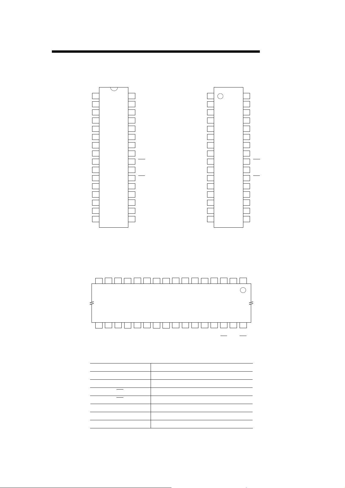
PIN CONFIGURATION (TOP VIEW)
MSM27C401CZ
1
Vpp
2
A16
3
A15
4
A12
A7
5
A6
6
A5
7
A4
8
A3
9
A2
10
A1
11
A0
12
D0
13
D1
14
D2
15
V
16 17
SS
32-pin DIP
32
31
30
29
28
27
26
25
24
23
22
21
20
19
18
V
CC
A18
A17
A14
A13
A8
A9
A11
OE
A10
CE
D7
D6
D5
D4
D3
1
Vpp
2
A16
3
A15
4
A12
A7
5
A6
6
A5
7
A4
8
A3
9
A2
10
A1
11
A0
12
D0
13
D1
14
D2
15
V
16 17
SS
32-pin SOP
32
31
30
29
28
27
26
25
24
23
22
21
20
19
18
V
CC
A18
A17
A14
A13
A8
A9
A11
OE
A10
CE
D7
D6
D5
D4
D3
Vpp A18
A16
A4
A5
A6
A7
A15
A12
32-pin TSOP
A3
A1
A2 D1
A0
D0
D2
V
PIN NAMES
A0 - A18 Address input
D0 - D7 Data output
CE
OE
V
CC
V
SS
V
PP
V
CC
A17
D3 D5 D7
D4 D6
SS
A13A8A9
A10
CE
FUNCTIONS
Chip enable
Output enable
Power supply voltage
GND
Program Power supply voltage
A11A14
12345678910111213141516
32313029282726252423222120191817
OE
2
Page 3
MSM27C401CZ
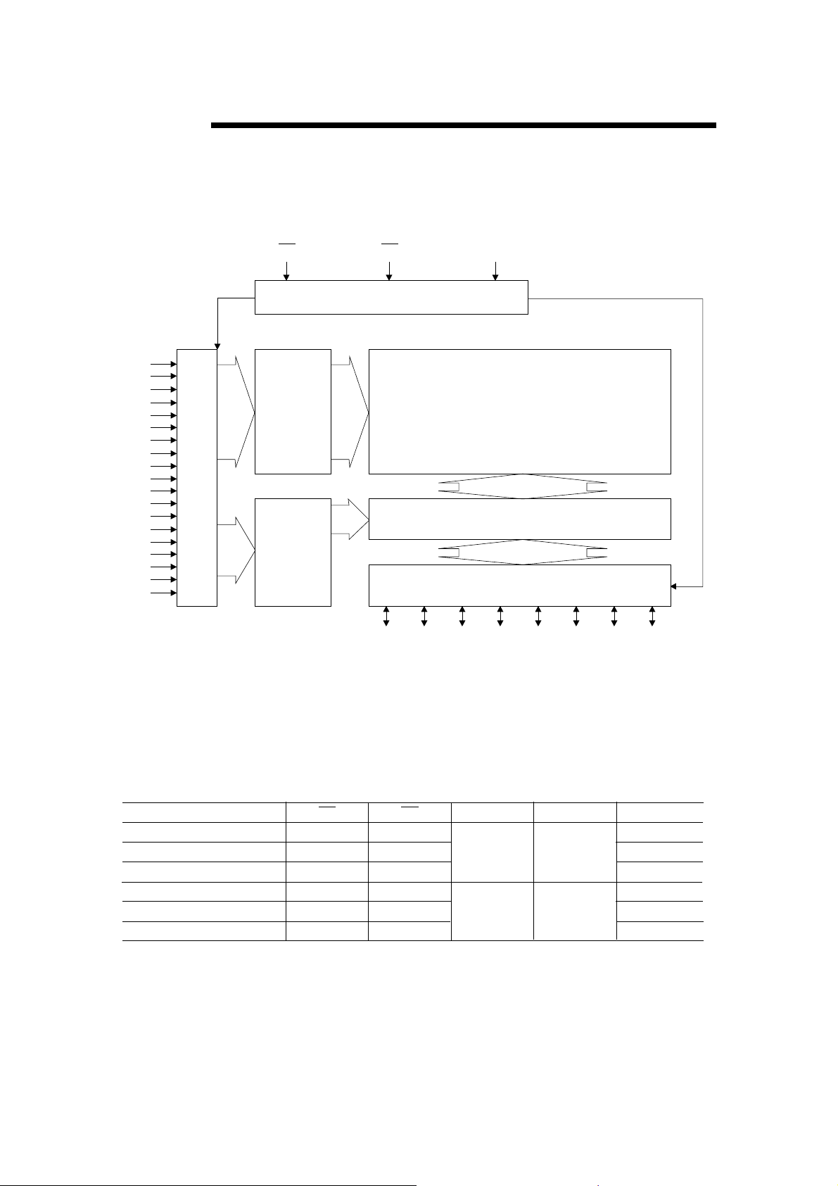
BLOCK DIAGRAM
A0
A1
A2
A3
A4
A5
A6
A7
A8
A9
A10
A11
A12
A13
A14
A15
A16
A17
A18
Address Buffer
CE V
OE
CE PGMOE
Memory Matrix
Row Decoder
524,288X8-Bit
Column Decoder
D0
D1 D2 D3 D4 D5 D6 D7
PP
Multiplexer
Output Buffer
FUNCTION TABLE
MODE
READ
OUTPUT DISABLE
STAND-BY
PROGRAM
PROGRAM INHIBIT
PROGRAM VERIFY
*: Don't Care
3
CE
L
L
H
L
H
H
OE
L
H
*
H
H
L
V
PP
*
11.5V
V
CC
2.7V to 5.5V
6.25V
D0 - D7
D
OUT
Hi-Z
Hi-Z
D
IN
Hi-Z
D
OUT
Page 4
ABSOLUTE MAXIMUM RATINGS
MSM27C401CZ
Parameter
Operating temperature under bias
Storage temperature
Input voltage
Output voltage
Power supply voltage
Program power supply voltage
Power dissipation per package
Symbol
Topr
T
stg
V
I
V
O
V
CC
V
PP
P
D
-
relative to V
-
SS
RECOMMENDED OPERATING CONDITIONS FOR READ
Parameter Symbol
VCC power supply voltage
VPP power supply voltage
Input "H" level
Input "L" level
Voltage is relative to Vss
V
CC
V
PP
V
IH
V
IL
Condition
VCC=2.7V - 5.5V
0 to 70
-55 to 125
+ 0.5
CC
(Ta=0 to 70°C)
Min. Max.
2.7
-0.5
Typ.
-
-
-
-
5.5
+0.5
V
CC
+0.52.2
V
CC
0.6-0.5
UnitValueCondition
°C
°C
V-0.5 to V
V-0.5 to VCC + 0.5
V-0.5 to 7
V-0.5 to 12.5
W1.0
Unit
V
V
V
V
4
Page 5
MSM27C401CZ
ELECTRICAL CHARACTERISTICS (Read operation)
DC Characteristics 1
Parameter
Input leakage current
Output leakage current
power supply current
V
CC
(Standby)
V
power supply current
CC
(Read)
V
power supply current
PP
Input "H" level
Input "L" level
Output "H" level
Output "L" level
Voltage is relative to Vss
Symbol
I
LI
I
LO
I
CS1
I
CS2
I
CCA
I
PP
V
IH
V
IL
V
OH
V
OL
VI=0 to Vcc
VO=0 to Vcc
CE=V
IL ,
tc=150ns
I
CE=V
CE=V
OE=V
V
PP=VCC
=-200µA
OH
=1mA
OL
-
-
CC
IH
=3V±0.3V, Ta=0 to 70°C)
(V
CC
Min. Max.
IH
2.0
-0.5 V
VCC-0.4
Typ.
-
-
-
-
-mA
-
-
-
-
-
-
-
-
-
-
-
-
10
10
10
15
10
VCC+0.5
0.6
-
0.4
UnitCondition
µA
µA
µA
1
mA
µA
V
V
VI
DC Characteristics 2
Parameter
Input leakage current
Output leakage current
V
power supply current
CC
(Standby)
V
power supply current
CC
(Read)
V
power supply current
PP
Input "H" level
Input "L" level
Output "H" level
Output "L" level
Voltage is relative to Vss
Symbol
I
LI
I
LO
I
CS1
I
CS2
I
CCA
I
PP
V
IH
V
IL
V
OH
V
OL
VI=0 to Vcc
VO=0 to Vcc
CE=V
IL ,
tc=120ns
I
CE=V
CE=V
OE=V
V
PP=VCC
=-200µA
OH
=1mA
OL
(V
=3.3V±0.3V, Ta=0 to 70°C)
CC
Min. Max.
CC
IH
IH
-
-
2.0
-0.5
VCC-0.4
Typ.
-
-
-
-
-mA
-
-
-
-
-
-
-
-
-
-
-
-
10
10
10
1
20
10
VCC+0.5
0.6
-
0.4
UnitCondition
µA
µA
µA
mA
µA
V
V
V
VI
5
Page 6

DC Characteristics 3
Parameter
Input leakage current
Output leakage current
V
power supply current
CC
(Standby)
V
power supply current
CC
(Read)
V
power supply current
PP
Input "H" level
Input "L" level
Output "H" level
Output "L" level
Voltage is relative to Vss
Symbol
I
LI
I
LO
I
CS1
I
CS2
I
CCA
I
PP
V
IH
V
IL
V
OH
V
OL
VO=0 to Vcc
CE=V
IL ,
tc=80ns
VI=0 to Vcc
CE=V
CC
CE=V
IH
OE=V
IH
V
PP=VCC
-
-
=-400µA
I
OH
=2.1mA
OL
MSM27C401CZ
(V
=5V±0.5V, Ta=0 to 70°C)
CC
Min. Max.
2.2
-0.5 V
2.4
Typ.
-
-
-
-
-mA
-
-
-
-
-
-
-
-
-
-
-
-
10
10
50
1
35
10
VCC+0.5
0.8
-
0.45
UnitCondition
µA
µA
µA
mA
µA
V
V
VI
AC Characteristics 1
Parameter
Access cycle time
Address access time
CE access time
OE access time
Output disable time
Output hold time
Symbol
T
C
T
ACC
T
CE
T
OE
T
CHZ
T
OHZ
T
OH
Measurement conditions
Input signal level
Input timing reference level
Output load
Output timing reference level
Output
-
CE=OE=V
OE=V
IL
CE=V
IL
OE=V
IL
CE=V
IL
CE=OE=V
0V/3V
0.8V/2.0V
50pF
0.8V/2.0V
1.7V
400
50pF
=3V±0.3V, Ta=0 to 70°C)
(V
CC
Min. Max.
150
IL
-
-
-
150
150
80
700
0
IL
0
65
-
UnitCondition
ns
ns
ns
ns
ns
ns
ns
6
Page 7

MSM27C401CZ
AC Characteristics 2
Parameter
Access cycle time
Address access time
CE access time
OE access time
Output disable time
Output hold time
Symbol
T
C
T
ACC
T
CE
T
OE
T
CHZ
T
OHZ
T
OH
-
CE=OE=V
OE=V
IL
CE=V
IL
OE=V
IL
CE=V
IL
CE=OE=V
=3.3V±0.3V, Ta=0 to 70°C)
(V
CC
Min. Max.
120
IL
-
-
-
120
120
70
600
0
IL
0
55
-
UnitCondition
ns
ns
ns
ns
ns
ns
ns
Measurement conditions
Input signal level
Input timing reference level
Output load
Output timing reference level
AC Characteristics 3
Parameter
Access cycle time
Address access time
CE access time
OE access time
Output disable time
Output hold time
Symbol
T
C
T
ACC
T
CE
T
OE
T
CHZ
T
OHZ
T
OH
Measurement conditions
Input signal level
Input timing reference level
Output load
Output timing reference level
0V/3V
0.8V/2.0V
100pF
0.8V/2.0V
-
CE=OE=V
OE=V
CE=V
OE=V
CE=V
CE=OE=V
IL
IL
IL
IL
IL
IL
0V/3V
0.8V/2.0V
1TTL gate + 100pF
0.8V/2.0V
=5V±0.5V, Ta=0 to 70°C)
(V
CC
Min. Max.
80
-
-
-
80
80
50
400
0
0
35
-
UnitCondition
ns
ns
ns
ns
ns
ns
ns
1.7V
400
Output
100pF
7
Page 8

TIMING CHART (READ CYCLE)
A0 - A18
CE
OE
MSM27C401CZ
t
C
t
t
CE
t
OE
OH
t
CHZ
D0 - D7
t
ACC
Valid Data
t
OHZ
Hi-ZHi-Z
8
Page 9

MSM27C401CZ
ELECTRICAL CHARACTERISTICS (Programming operation)
DC Characteristics
Parameter
Input leakage current
V
power supply current (Program)
PP
VCC power supply current
Input "H" level
Input "L" level
Output "H" level
Output "L" level
Program voltage
power supply voltage
V
CC
Voltage is relative to Vss
AC Characteristics
Parameter
Address set-up time
OE set-up time
Data set-up time
Address hold time
Data hold time
Output float delay from OE
voltage set-up time
V
PP
Program pulse width
Data valid from OE
Symbol
I
LI
I
PP2
I
CC
V
IH
V
IL
V
OH
V
OL
V
PP
V
CC
Symbol
T
AS
T
OES
T
DS
T
AH
T
DH
T
DFP
T
VS
T
PW
T
OE
Condition
V
+0.5V
I=VCC
CE=V
IL
-
-
=-400µA
OH
=2.1mA
I
OL
-
-
(Vcc=6.25V
Condition
-
-
-
-
-
-
-
-
Min. Max.
-
-
-
2.2
-0.5
2.4
-
6.0
±0.25V,V
=11.5V±0.25V,Ta=25°C±5°C)
pp
Min. Max.
2
2
2
0
2 µs
0
2
-
Typ.
-
-
--
-
-
-
-
11.5
6.25
Typ.
-
-
--
-
-
-
25
-
(Ta=25°C
10
50
80
V
+0.5
CC
0.8
-
0.45
11.7511.25
6.5
-
-
-
-
-
130
-
2723
150
±5°C)
Unit
µA
mA
mA
V
V
VI
V
V
V
Unit
µs
µs
µs
µs
ns-
µs
µs
ns
9
Page 10

Programming Waveform
A0 - A18
t
CE
AS
t
PW
t
OES
t
t
DFP
MSM27C401CZ
AH
OE
D0 - D7
V
PP
PIN Capacitance
Parameter
Input
Output
t
DS
D
IN
t
VS
Program
t
DH
t
OE
D
OUT
Program Verify
(VCC=5V, Ta=25°C, f=1MHz)
Symbol
C
IN
C
OUT
Condition
VI=0V
=0V
V
O
Min. Max.
-
Typ.
-
--
12
15
Unit
pF
10
Page 11

MSM27C401CZ
High Speed Programming Algorithm ( I )
Start
First Address
VCC=6.25V
VPP=11.5V
X=0
Increment Address
NG
NO
X=10 ?
NO
Program 25µs
X=X+1
Verify (One Byte)
PASS
Last Address ?
YES
VCC=5.5V
V
=5.5V
PP
Compare All
YES
NG
11
PASS
VCC=2.7 (4.5V)
V
=2.7 (4.5V)
PP
Compare All
PASS
Device Passed
NG
Device Failed
Page 12

High Speed Programming Algorithm ( II )
First Address
VCC=6.25V
VPP=11.5V
Program 25µs
MSM27C401CZ
Start
Increment Address
Increment Address
NO
Last Address ?
First Address
Verify (One Byte)
NO
Last Address ?
Compare All
YES
X=0
PASS
YES
VCC=5.5V
V
=5.5V
PP
NG
NG
X=X+1
YES
X=10 ?
NO
Program 25µs
PASS
VCC=2.7V (4.5V)
V
=2.7V (4.5V)
PP
Compare All
PASS
Device Passed
NG
Device Failed
12
Page 13

Semiconductor
NOTICE
The information contained herein can change without notice owing to product and/or technical improvements. Before using the product, please make sure that the information being referred to is up-todate.
The outline of action and examples for application circuits described herein have been chosen as an
explanation for the standard action and performance of the product. When planning to use the product,
please ensure that the external conditions are reflected in the actual circuit, assembly, and program
designs.
When designing your product, please use our product below the specified maximum ratings and within
the specified operating ranges including, but not limited to, operating voltage, power dissipation, and
operating temperature.
Oki assumes no responsibility or liability whatsoever for any failure or unusual or unexpected operation resulting from misuse, neglect, improper installation, repair, alteration or accident, improper handling, or unusual physical or electrical stress including, but not limited to, exposure to parameters beyond the specified maximum ratings or operation outside the specified operating range.
Neither indemnity against nor license of a third party’s industrial and intellectual property right, etc. is
granted by us in connection with the use of the product and/or the information and drawings contained
herein. No responsibility is assumed by us for any infringement of a third party’s right which may result
from the use thereof.
The products listed in this document are intended for use in general electronics equipment for commercial applications (e.g., office automation, communication equipment, measurement equipment, consumer
electronics, etc.). These products are not authorized for use in any system orapplication that requires
special or enhanced quality and reliability characteristics nor in any system or application where the
failure of such system or application may result in the loss or damage of property, or death or injury to
humans. Such applications include, but are not limited to, traffic and automotive equipment, safety devices, aerospace equipment, nuclear power control, medical equipment, and life-support systems.
Certain products in this document may need government approval before they can be exported to particular countries. The purchaser assumes the responsibility of determining the legality of export of these
products and will take appropriate and necessary steps at their own expense for these.
No part of the contents cotained herein may be reprinted or reproduced without our prior permission.
All brand, company and product names are the trademarks or registered trademarks of their respective
owners.
Copyright 1998 Oki Electric Industry Co., Ltd.
Page 14

ADDRESSES & SEMICONDUCTOR WEB SITES
OKI Electric Industry Co., Ltd.OKI Electric Industry Co., Ltd.
OKI Electric Industry Co., Ltd.,
OKI Electric Industry Co., Ltd.OKI Electric Industry Co., Ltd.
Device Business Group,
10-3, Shibaura, 4-chome,
Minato-ku, Tokyo 108, Japan,
Tel.: +81-(0)3-5445-6327,
Fax.: +81-(0)3-5445-6328,
http://www.oki.co.jp/OKI/DBG/english/index.htm
(NOTE: URL is case sensitive)
OKI Semiconductor GroupOKI Semiconductor Group
OKI Semiconductor Group,
OKI Semiconductor GroupOKI Semiconductor Group
785 North Mary Avenue,
Sunnyvale, CA 94086, U.S.A.,
Tel.: +1-408-720-1900,
Fax.: +1-408-720-1918,
http://www.okisemi.com/
OKI Electric Europe GmbHOKI Electric Europe GmbH
OKI Electric Europe GmbH,
OKI Electric Europe GmbHOKI Electric Europe GmbH
Head Office Europe,
Hellersbergstrasse 2,
D-41460 Neuss, Germany,
Tel: +49-2131-15960,
Fax: +49-2131-103539,
http://www.oki-europe.de/
OKI Electronics (Hong Kong) Ltd.OKI Electronics (Hong Kong) Ltd.
OKI Electronics (Hong Kong) Ltd.,
OKI Electronics (Hong Kong) Ltd.OKI Electronics (Hong Kong) Ltd.
Suite 1901-1&19, Tower 3,
China Hong Kong City,
33 Canton Road, Tsimshatsui,
Kowloon, Hong Kong,
Tel.: +852-2-736-2336,
Fax.: +852-2-736-2395
OKI Semiconductor (Asia) Pte. Ltd.OKI Semiconductor (Asia) Pte. Ltd.
OKI Semiconductor (Asia) Pte. Ltd.,
OKI Semiconductor (Asia) Pte. Ltd.OKI Semiconductor (Asia) Pte. Ltd.
78 Shenton Way 09-01,
Singapore 0207,
Tel.: +65-221-3722,
Fax.: +65-323-5376
OKI Semiconductor (Asia) Pte. Ltd.OKI Semiconductor (Asia) Pte. Ltd.
OKI Semiconductor (Asia) Pte. Ltd.,
OKI Semiconductor (Asia) Pte. Ltd.OKI Semiconductor (Asia) Pte. Ltd.
Taipei Branch,
7th Fl. No.260, Tun Hwa North Road,
Taipei, Taiwan, R.O.C.,
Sumitomo-Flysun Building,
Tel.: +886-2-2719-2561,
Fax.: +886-2-2715-2892
http://www.oki.net.tw/
For further information, please contact:
People To People Technology
 Loading...