

Page 1
D
ATA SHEET
OKI ASIC PRODUCTS
MSM13Q/14Q000
0.35 µm Sea of Gates Arrays
November 1999
Page 2

■ ■
–––––––––––––––––––––––––––––––––––––––––––––––––––––––––––––––––––––––––––––––––––––––––––
Oki Semiconductor
Page 3

MSM13Q0000/14Q0000
0.35 µm Sea of Gates Arrays
DESCRIPTION
Oki’s 0.3 5 µm ASIC products deliver ultra-high performance and high density at low power dissipation.
The MSM13Q0000/14Q0000 series devices (referred to as “MSM13Q/14Q”) are implemented with the
industry-standard Cell-Based Array (CBA) architecture in a Sea-of-Gates (SOG) structure. Built in a
0.35 µm drawn CMOS technology (with an L-Effective of 0.27 µm), these SOG devices are available in
three layers (MSM13Q) and four layers (MSM14Q) of metal. The semiconductor process is adapted from
Oki’s production-proven 64-Mbit DRAM manufacturing process.
The MSM13Q/14Q Series contains 6 arrays each, offering over 1 million raw gates and 352 I/O pads. Up
to 66% and 90% of the raw gates can be used for the 3-layer and 4-layer arrays, respectively. Oki’s 0.35
µm family is optimized for 3-V core operation with optimized 3-V I/O buffers and 5-V tolerant 3-V buffers. These SOG products are designed to fit the most popular plastic quad flat packs (QFPs), thin QFPs
(TQFPs) , and plastic ball grid array (PBGA) packages.
The MSM13Q/14Q Series uses the popular CBA architecture from Silicon Architects of Synopsys which
mixes two types of cells (8-transistor compute cells and 4-transistor drive cells) on the same die to deliver
high gate density and high drives. The CBA is supported by a rich macro library, optimized for synthesis.
Memory blocks are efficiently created by Oki’s memory compilers to generate single- and dual-port
RAM’s in high-density and low-power configurations with synchronous RAM options.
As such, the MSM13Q/14Q series is well suited to memory-intensive designs with high production volumes approaching the real estate and cost savings of standard cells. At the same time, its SOG architecture allows rapid prototyping turnaround times. Thus, Oki’s MSM13Q/14Q family offers the best of two
worlds: quick prototyping of a gate array and low production cost of a standard cell.
Oki’s 0.35 µm ASIC products are supported by leading-edge CAD tools including a synthesis-linked
floorplanner, motive static timing analyzer, and H-clock tree methodology. They are further supported
by specialized macrocells including phase-locked loop (PLL), pseudo-emitter coupled logic (PECL),
peripheral component interconnect (PCI), universal synchronous receiver/transmitter (UART) cells, and
ARM7TDMI RISC cores.
FEATURES
• 0.35 µm drawn 3- and 4-layer metal CMOS
• Optimized 3.3-V core
• Optimized 3-V I/O and 3-V I/O that is 5-V
tolerant
• CBA SOG architecture
• Over 1.0M raw gates and 352 pads
• User-configurable I/O with V
state, and 1- to 24-mA options
• Slew-rate-controlled outputs for low-radiated
noise
• H-clock tree cells which reduce the maximum
skew for clock signals
, VDD, TTL, 3-
SS
• User-configurable single and dual-port;
synchronous or asynchronous memories
• Specialized macrocells including PLL, PECL,
PCI, UART, and ARM7TDMI
• Floorplanning for front-end simulation, backend layout controls, and link to synthesis
• Joint Test Action Group (JTAG) boundary scan
and scan-path ATPG
• Support for popular CAE systems, including
Cadence, IKOS, Mentor Graphics, Synopsys,
Viewlogic, and Zycad
1Oki Semiconductor
Page 4
■
MSM13Q0000/14Q0000 ■ ––––––––––––––––––––––––––––––––––––––––––––––––––––––––––––––––––––––––
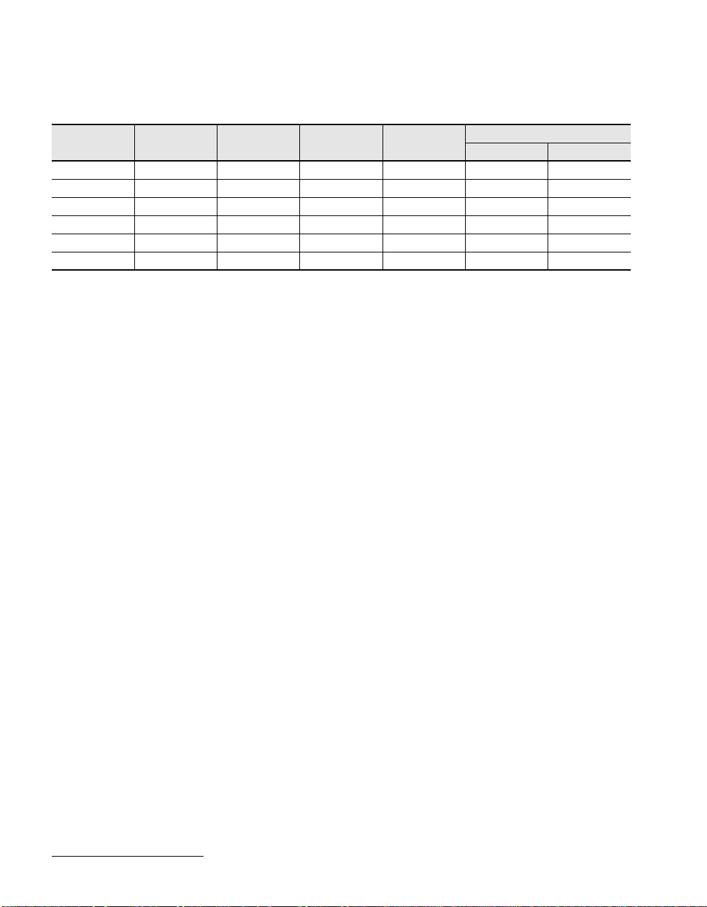
MSM13Q/14Q FAMILY LISTING
MSM13Q/14Q
Series
0150 144 157,192 105,319 143,045 196 802
0230 176 242,400 152,712 208,464 240 1,010
0340 208 346,176 204,244 276,941 288 1,202
0530 256 536,400 289,656 391,572 360 1,490
0840 320 847,048 415,054 567,522 452 1,874
1020 352 1,033,000 475,180 650,790 500 2,066
PAD No.
Raw Gate
(Gates)
Usable Gate
M13Q(3LM)
Usable Gate
M14Q(4LM)
Raw Gate
Row Column
ARRAY ARCHITECTURE
The primary components of a 0.35 µm MSM13Q/14Q circuit include:
• I/O base cells
• Configurable I/O pads for VDD, VSS, or I/O (optimized 3-V I/O and 3-V I/O that is 5-V tolerant)
•V
and VSS pads dedicated to wafer probing
DD
• Separate power bus for output buffers
• Separate power bus for internal core logic and input buffers
• Core base modules containing three compute cells for each drive cell
• Isolated gate structure for reduced input capacitance and increased routing flexibility
Each array has 24 dedicated corner pads for power and ground use during wafer probing, with 4 pads
per corner. The arrays also have separate power rings for the internal core functions (V
and output drive transistors (V
DDO
and V
SSO
).
The array architecture uses optimally sized transistors to efficiently implement logic and memory in a
metal programmable technology. CBA uses two types of cells: compute cells and drive cells. The compute cell employs four PMOS and four NMOS trasnsistors whose sizes are optimized for logic and memory implementations as shown in
Figure 1
. The quantity and size of the transistors in a compute cell are
carefully selected to maximize the efficiency of most commonly used functions in VLSI design. The drive
cell consists of two large PMOS pull-up transistors and two large pull-down transistors. The compute
and drive cells are tiled to create a channelless core array, with three comput cells for each drive cell as
shown in
Figure 2
. The 3:1 ratio of compute to drive cells was selected for optimal implementation of
emerging applications. Macrocells are created using either compute cells, drive cells, or combinations of
compute and drive cells.
DDC
and V
SSC
)
2 Oki Semiconductor
Page 5

––––––––––––––––––––––––––––––––––––––––––––––––––––––––––––––––––––––– ■ MSM13Q0000/14Q0000
Compute Cell Compute Cell Compute Cell Drive Cell
Figure 1. Base Cell Consisting of Three Compute Cells and One Drive Cell
■
Compute Cell Drive Cell
Figure 2. Core Array with Base Cell Mirrored Horizontally and Ver tically
3Oki Semiconductor
Page 6

■
MSM13Q0000/14Q0000 ■ ––––––––––––––––––––––––––––––––––––––––––––––––––––––––––––––––––––––––
ELECTRICAL CHARACTERISTICS
Absolute Maximum Ratings (VSS = 0 V, Tj = 25°C)
Parameter
Power supply voltage V
Input voltage Normal buffers V
5-V tolerant V
Output voltage Normal buffers V
5-V tolerant V
Input current Normal buffers I
5-V tolerant I
Output current per I/O Normal buffers IO I
5-V tolerant I
Storage temperature T
Symbol Conditions Rated Value Unit
DD
O
O
I
I
O
stg
[1]
-0.3 to +4.6 V
I
I
-0.3 to VDD+0.3
-0.3 to 6.0
-0.3 to VDD+0.3
-0.3 to 6.0
-10 to +10
-6 to +6
= 1, 2, 4, 6, 8, 12, 24 mA -24 to +24
O
I
= 2, 4, 6, 8, 12 mA -8 to +8
O
– -65 to +150 °C
V
V
mA
mA
1. Permanent device damage may occur if ABSOLUTE MAXIMUM RATINGS are exceeded. Functional operation should be restricted to the conditions
in the other specifications of this data sheet. Exposure to absolute maximum rating conditions for extended periods may affect device reliability.
Recommended Operating Conditions (VSS = 0 V)
Parameter
Power supply voltage V
Junction temperature T
Symbol Rated Value Unit
(3 V) +3.0 to +3.6 V
DD
j
-40 to +85 °C
4 Oki Semiconductor
Page 7

––––––––––––––––––––––––––––––––––––––––––––––––––––––––––––––––––––––– ■ MSM13Q0000/14Q0000
DC Characteristics (VDD = 3.0 to 3.6 V, VSS = 0 V, Tj = -40°C to +85°C)
[1]
[2]
Max.
Unit
V
µA
–
µA
µA
µA
Parameter
High-level input voltage Normal buffer V
5-V tolerant V
Low-level input voltage Normal buffer V
5-V tolerant V
TTL- level Schmitt trigger input
Normal buffer V
threshold voltage
5-V tolerant V
High-level output voltage Normal buffer V
5-V tolerant V
Low-level output voltage Normal buffer V
5-V tolerant V
High-level input current
Normal buffer
5-V tolerant I
Low-level input current Normal buffer I
5-V tolerant I
3-state output leakage current Normal buffer I
5-V tolerant I
Stand-by current
[3]
1. JEDEC Compatible; JESD8-1A LVTTL.
2. Typical condition is
VDD = 3.3 V and Tj = 25oC
3. RAM/ROM should be in powerdown mode.
Symbol Conditions
IH
IH
TTL input -0.3 – 0.8
IL
TTL input -0.3 – 0.8
IL
t+
TTL input
V
t-
∆
VtVt+ - V
t+
V
t-
∆
VtVt+ - V
OHIOH
t-
TTL 5-V tolerant input
t-
= -100 µA V
IOH = -1, -2, -4, -6, -8, -12, -24 mA 2.4 – –
OHIOH
= -100 µA V
IOH = -1, -2, -4, -6, -8, -12 mA 2.4 – –
OLIOL
OLIOL
= 100 µA – – 0.2
I
= 1, 2, 4, 6, 8, 12, 24mA – – 0.4
OL
= 100 µA – – 0.2
IOL = 1, 2, 4, 6, 8, 12 mA – – 0.4
I
VIH = V
IH
DD
VIH = VDD (50-kΩ pull-down) 10 66 200
VIH = V
IH
DD
VIH = VDD (50-kΩ pull-down) 10 66 200
VIL = V
IL
SS
VIL = VSS (50-kΩ pull-up) -200 -66 -10
VIL = VSS (3-kΩ pull-up) -3.3 -1.1 -0.3 mA
VIL = V
I
IL
OZH
OZL
SS
VOH = V
DD
= VDD (50-kΩ pull-down) 10 -66 200
V
OH
VOL = V
SS
V
= VSS (50-kΩ pull-up) -200 -66 -10
OL
VOL = VSS (3-kΩ pull-up) -3.3 -1.1 -0.3 mA
VOH = V
OZH
I
I
DDQ
OZL
DD
V
= V
(50-kΩ pull-down) 10 66 200
OH
DD
VOL = V
SS
Output open, VIH = VDD, VIL = V
on a typical process.
Rated Value
Min. Typ
2.0 – VDD + 0.3
2.0 – 5.5
– 1.5 2.0
0.7 1.0 –
0.4 0.5 –
– 1.5 2.0
0.7 1.0 –
0.4 0.5 –
- 0.2 – –
DD
- 0.2 – –
DD
– 0.1 10
– 0.1 10
-10 -0.1 -
-10 -0.1
– 0.1 10
-10 -0.1 –
– 0.1 10
-10 -0.1 –
SS
Design Dependent µA
■
5Oki Semiconductor
Page 8

■ MSM13Q0000/14Q0000 ■ ––––––––––––––––––––––––––––––––––––––––––––––––––––––––––––––––––––––––
AC Characteristics (VDD = 3.3 V, VSS = 0 V, Tj = 25°C)
Driving
Parameter
Internal gate
propagation delay
Inverter 1X F/O = 2, L = 0 mm
Type Conditions
2X 0.068
V
4X 0.062
2-input NAND 1X 0.14
2X 0.13
2-input NOR 1X 0.16
2X 0.14
Inverter 1X F/O = 2, L = 1 mm
2X 0.13
V
4X 0.097
2-input NAND 1X 0.28
2X 0.20
2-input NOR 1X 0.34
2X 0.24
Toggle frequency F/O= 1, L = 0 mm 1040 MHz
Input buffer
propagation delay
Output buffer
propagation delay
TTL level normal input buffer F/O = 2,L = 1 mm 0.35
TTL level 5-V tolerant buffer 0.64
Push-pull
Normal output
buffer
4 mA CL = 20pF 2.15
8 mA CL= 50 pF 2.25
12 mA CL = 100 pF 2.82
3-state
4 mA CL = 20 pF 2.41
5-V tolerant
buffer
Output buffer
transition times
[4]
Push-pull
Normal output
12 mA CL = 100 pF 4.68 (r)
buffer
3-state
4 mA CL = 20 pF 3.53 (r)
5-V tolerant
buffer
1. Input transition time in 0.2 ns / 3.3 V.
2. Typical condition is V
3. Rated value is calculated as an average of the L-H and H-L delay times of each macro type on a typical process.
4. Output rising and falling times are both specified over a 10 to 90% range.
= 3.3 V and Tj = 25oC.
DD
DD
DD
[1] [2]
= 3.3 V
= 3.3 V
Rated Value
0.082
0.19
3.48 (f)
3.24 (f)
[3]
Unit
ns
ns
6 Oki Semiconductor
Page 9

––––––––––––––––––––––––––––––––––––––––––––––––––––––––––––––––––––––– ■ MSM13Q0000/14Q0000 ■
MACRO LIBRARY
Oki Semiconductor supports a wide range of macrocells and macrofunctions, ranging from simple hard
macrocells for basic Boolean operations to large, user-parameterizable macrofunctions. The following
figure illustrates the main classes of macrocells and macrofunctions available.
Examples
Basic Macrocells
NANDs
NORs
EXORs
Latches
Flip-Flops
Combinational Logic
Macro Library
Macrocells
Macrofunctions
Basic Macrocells
with Scan test
Clock Tree Driver
Macrocells
3V, 5V Tolerant
Output Macrocells
MSI Macrocells
Mega/Special
Macrocells
3-V, 5-V Tolerant
Input Macrocells
3-V, 5-V Tolerant
Bi-Directional
Macrocells
Oscillator
Macrocells
Memory
Macrocells
MSI
Macrofunctions
[1] Under development
Flip-Flops
3-State Outputs
Push-Pull Outputs
PECL Outputs
Counters
Shift Registers
UART
[1]
PLL
Inputs
Inputs with Pull-Ups
I/O
PCI I/O
Gated Oscillators
CBA RAMs:
Single-Port RAMs (asynchronous or synchronous)
Dual-Port RAMs (asynchronous)
4-Bit Register/Latches
Open Drain Outputs
Slew Rate Control Outputs
PCI Outputs
USB Controller
Ethernet Controller
Inputs with Pull-Downs
PECL Inputs
I/O with Pull-Downs
I/O with Pull-Ups
Figure 3. Oki Macrocell and Macrofunction Library
7Oki Semiconductor
Page 10

■ MSM13Q0000/14Q0000 ■ ––––––––––––––––––––––––––––––––––––––––––––––––––––––––––––––––––––––––
Macrocells for Driving Clock Trees
Oki offers H-clock-tree drivers that minimize clock skew. The advanced layout software uses dynamic
driver placement and sub-trunk allocation to optimize the clock-tree implementation for a particular circuit. Features of the H-clock-tree driver-macrocells include:
• True RC back annotation of the clock network
• Automatic fan-out balancing
• Dynamic sub-trunk allocation
• Single clock tree driver logic symbol
• Automatic branch length minimization
• Dynamic driver placement
• Allows multiple clock trees
8 Oki Semiconductor
Clock
Figure 4. H-Clock-Tree Structure
Page 11

––––––––––––––––––––––––––––––––––––––––––––––––––––––––––––––––––––––– ■ MSM13Q0000/14Q0000 ■
OKI ADVANCED DESIGN CENTER CAD TOOLS
Oki’s advanced design center CAD tools include support for the following:
• Floorplanning for front-end simulation, back-end layout control, and link to synthesis
• Clock tree structures improve first-time silicon success by eliminating clock skew problems
• JTAG Boundary scan support
• Power calculation which predicts circuit power under simulation conditions to accurately model
package requirements (in development)
Table 1: CAD Design Tools
Vendor Platform Operating System
Cadence HP9000, 7xx
IKOS HP9000, 7xx,
Mentor Graphics™ HP9000, 7xx
Synopsys
(Interface to Mentor
Graphics, VIEWLogic)
Model Technology, Inc.
(MTI)
VIEWLogic PC
IBM RS6000
® [2]
Sun
[2]
Sun
[2]
Sun
IBM RS6000
HP9000, 7xx
[2]
Sun
HP9000, 7xx
[2]
Sun
PC
[2]
Sun
HP-UX
AIX
SunOS, Solaris
HP-UX, SunOS, Solaris NSIM
HP-UX
SunOS, Solaris
AIX
HP-UX
SunOS, Solaris
HP-UX
SunOS, Solaris.
Win95/NT™
Windows™,
Windows NT™
SunOS, Solaris
1. Contact Oki Application Engineering for current software versions.
2. Sun or Sun-compatible.
3. Sun and HP platform only.
[1]
Vendor Software/Revision
HDL/VHDL Compiler™
Workview Office™
ViewSim™ with VSO
Composer™
Verilog™
Veritime™
Verifault™
Synergy™
Concept™
Leapfrog™
Gemini/Voyager
IDEA™
QuickVHDL
QuickSim II™
QuickPath™
QuickFault™
QuickGrade™
AutoLogic™
DFT Advisor
Design Compiler™
Test Compiler™
VSS™
V-System VHDL Simulation
Powerview™
Vantage Optium
Motive
[1]
[3]
Description
Design capture
Simulation
Timing analysis
Fault grading
Design synthesis
Design capture
VHDL simulation
Simulation
Design capture
VHDL simulation
Logic simulation
Timing analysis
Fault grading
Fault grading
Design synthesis
Test synthesis
Compilation
Design synthesis
Test synthesis
VHDL simulation
Design capture
Simulation
VHDL simulation
Timing analysis
Design synthesis
Simulation
9Oki Semiconductor
Page 12

■ MSM13Q0000/14Q0000 ■ ––––––––––––––––––––––––––––––––––––––––––––––––––––––––––––––––––––––––
Design Process
The following figure illustrates the overall IC design process and shows the three main interface points
between external design houses and Oki ASIC Application Engineering.
[5]
Schematics
VHDL/HDL Description
Test Vectors
Level 1
[1]
CDC
Floorplanning
Netlist Conversion
(EDIF 200)
Scan Insertion (Optional)
[1]
CDC
Floorplanning
Layout
Verification
(Cadence DRACULA)
Post-Layout Simulation
(Cadence Verilog)
Synthesis
Floorplanning
Gate-Level Simulation
Pre-Layout Simulation
(Cadence Verilog)
[6]
Fault Simulation
( Zycad)
[2]
LSF
Test Vector Conversion
Pattern Generation
(Synopsys Test Compiler)
[4]
(Oki TPL
[3]
TDC
Automatic Test
)
Level 2
Level 2.5
Level 3
CAE Front-End
[5]
Oki Interface
[5]
Manufacturing
Prototype
Test Program
[1] Oki’s Circuit Data Check (CDC) program verifies logic design rules.
[2] Oki’s Link to Synthesis Floorplanning (LSF) toolset transfers post-floorplanning timing for resynthesis.
[3] Oki’s Test Data Check (TDC) program verifies test vector rules.
[4] Oki’s Test Pattern Language (TPL).
[5] Alternate Customer-Oki design interfaces available in addition to standard level 2.
[6] Standard design process includes fault simulation.
10 Oki Semiconductor
Conversion
Figure 5. Oki’s Design Process
Page 13

––––––––––––––––––––––––––––––––––––––––––––––––––––––––––––––––––––––– ■ MSM13Q0000/14Q0000 ■
Automatic Test Pattern Generation
Oki’s 0.35 µm ASIC technologies support Automatic Test Pattern Generation (ATPG) using full scanpath design techniques, including the following:
• Increases fault coverage ≥95%
• Uses Synopsys Test Compiler
• Inserts scan structures automatically
• Connects scan chains
• Traces and reports scan chains
• Checks for rule violations
• Generates complete fault reports
• Allows multiple scan chains
• Supports vector compaction
ATPG methodology is described in detail in Oki’s 0.35 µm Scan Path Application Note.
Combinational Logic
A B
FD1AS FD1AS
Scan Data In
D
C
SD
SSQQN
D
SD
SS
C
Scan Data OutQ
QN
Scan Select
Figure 6. Full Scan Path Configuration
Floorplanning Design Flow
Oki offers three floorplanning tools for high-density ASIC design. The two main purposes for Oki’s floorplanning tool are to:
• Ensure conformance of critical circuit performance specifications
• Shorten overall design turnaround time (TAT)
The supported floorplanners are: Cadence DP3, Gambit GFP, and Oki’s internal floorplanner.
In a traditional design approach with synthesis tools, timing violations after prelayout simulation are
fixed by manual editing of the netlist. This process is difficult and time consuming. Also, there is no
physical cluster information provided in the synthesis tool, and so it is difficult to synthesize logic using
predicted interconnection delay due to wire length. Therefore, synthesis tools may create over-optimized
results.
To minimize these problems, Synopsys proposed a methodology called Links to Layout (LTL). Based on
this methodology, Oki developed an interface between Oki’s floorplanners and the Synopsys environment, called Link Synopsys to Floorplanner (LSF). Because not all Synopsys users have access to the Synopsys Floorplan Management tool, Oki developed the LSF system to support both users who can access
11Oki Semiconductor
Page 14

■ MSM13Q0000/14Q0000 ■ ––––––––––––––––––––––––––––––––––––––––––––––––––––––––––––––––––––––––
Synopsys Floorplan Management and users who do not have access to Synopsys Floorplan Management.
More information on OKI’s floorplanning capabilities is available in Oki’s Application Note, Using Oki’s
Floorplanner: Standalone Operation and Links to Synopsys.
Incremental
Optimization with
Initial Synthesis
Gate Level
Netlist
(EDIF)
Oki RC
PDEF (Synopsys)
Wire Load Model (Synopsys)
Net Capacitance (Synopsys
Script (Synopsys)
Delay
(SDF)
HDL Entry
SynthesisConstraints
Constraints Met?
Yes
Initial Floorplan
Invoke Export on
Floorplanner
Invoke Delay
Load
Back-Annotation Files
No
Physical Information
No
Constraints Met?
Invoke Import on
Yes
Floorplanner
Incremental
Floorplan
PDEF
(Synopsis)
Gate Level
Netlist
(EDIF)
= In Synopsys DC/DA
= In Floorplanner
12 Oki Semiconductor
Constraints Met?
Yes
To Simulation and P&R
No
Figure 7. LSF System Design Flow
Timing Optimization
Page 15

––––––––––––––––––––––––––––––––––––––––––––––––––––––––––––––––––––––– ■ MSM13Q0000/14Q0000 ■
IEEE JTAG Boundary Scan Support
Boundary scan offers efficient board-level and chip-level testing capabilities. Benefits resulting from
incorporating boundary-scan logic into a design include:
• Improved chip-level and board-level testing and failure diagnostic capabilities
• Support for testing of components with limited probe access
• Easy-to-maintain testability and system self-test capability with on-board software
• Capability to fully isolate and test components on the scan path
• Built-in test logic that can be activated and monitored
• An optional Boundary Scan Identification (ID) Register
Oki’s boundary scan methodology meets the JTAG Boundary Scan standard, IEEE 1149.1-1990. Either the
customer or Oki can perform boundary-scan insertion. More information is available in Oki’s JTAG
Boundary Scan Application Note. (Contact the Oki Application Engineering Department for interface
options.)
13Oki Semiconductor
Page 16

■ MSM13Q0000/14Q0000 ■ ––––––––––––––––––––––––––––––––––––––––––––––––––––––––––––––––––––––––
PACKAGE OPTIONS
TQFP & LQFP Package Menu
Base Array
MSM...
13Q/14Q0150 144
13Q/14Q0230 176
13Q/14Q0340 208
I/O Pads
[1]
64 80 100 144 176 208
●●●●
●●●●●
●●●●●●
13Q/14Q0530 256
13Q/14Q0840 320
13Q/14Q1020 352
Body Size (mm) 10 x 10 12 x 12 14 x 14 20 x 20 24 x 24 28 x 28
Lead Pitch (mm) 0.5 0.5 0.5 0.5 0.5 0.5
1. I/O Pads can be used for input, output, bi-directional, power, or ground.
● = Available now; ❍ = In development
PQFP Package Menu
Base Array
MSM...
13Q/14Q0150 144
13Q/14Q0230 176
13Q/14Q0340 208
13Q/14Q0530 256
13Q/14Q0840 320
13Q/14Q1020 352
Body Size (mm) 28 x 28 28 x 28 28 x 28 32 x 32
Lead Pitch (mm) 0.80 0.65 0.50 0.50
1. I/O Pads can be used for input, output, bi-directional, power, or ground.
● = Available now; ❍ = In development
I/O Pads
[1]
TQFP LQFP
●●●❍●
●❍●●
❍●●
PQFP (42 Alloy) PQFP (Cu-Alloy)
128 160 208 240
❍
❍❍
●●
●●●
●●●❍
❍●●❍
14 Oki Semiconductor
Page 17

––––––––––––––––––––––––––––––––––––––––––––––––––––––––––––––––––––––– ■ MSM13Q0000/14Q0000 ■
BGA Package Menu
Base Array
MSM...
13Q/14Q0150 144
13Q/14Q0230 176
13Q/14Q0340 208
13Q/14Q0530 256
13Q/14Q0840 320
13Q/14Q1020 352
Body Size (mm) 27 x 27 35 x 35
Ball Pitch (mm) 1.27 1.27
1. I/O Pads can be used for input, output, bi-directional, power, or ground.
● = Available now; ❍ = In development
I/O Pads
[1]
256 352
●
●
●
●●
●●
15Oki Semiconductor
Page 18

■ MSM13Q0000/14Q0000 ■ ––––––––––––––––––––––––––––––––––––––––––––––––––––––––––––––––––––––––
Notes:
16 Oki Semiconductor
Page 19

The information contained herein can change without notice owing to product and/or technical improvements.
Please make sure before using the product that the information you are referring to is up-to-date.
The outline of action and examples of application circuits described herein have been chosen as an explanation of the standard action
and performance of the product. When you actually plan to use the product, please ensure that the outside conditions are reflected in
the actual circuit and assembly designs.
Oki assumes no responsibility or liability whatsoever for any failure or unusual or unexpected operation resulting from misuse, neglect,
improper installation, repair, alteration or accident, improper handling, or unusual physical or electrical stress including, but not limited
to, exposure to parameters outside the specified maximum ratings or operation outside the specified operating range.
Neither indemnity against nor license of a third party's industrial and intellectual property right,etc.is granted by us in connection with
the use of product and/or the information and drawings contained herein. No responsibility is assumed by us for any infringement of a
third party's right which may result from the use thereof.
When designing your product, please use our product below the specified maximum ratings and within the specified operating ranges,
including but not limited to operating voltage, power dissipation, and operating temperature.
The products listed in this document are intended for use in general electronics equipment for commercial applications (e.g.,office
automation, communication equipment, measurement equipment, consumer electronics, etc.).These products are not authorized for
use in any system or application that requires special or enhanced quality and reliability characteristics nor in any system or application
where the failure of such system or application may result in the loss or damage of property or death or injury to humans. Such
applications include, but are not limited to: traffic control, automotive, safety, aerospace, nuclear power control, and medical, including
life support and maintenance.
Certain parts in this document may need governmental approval before they can be exported to certain countries. The purchaser
assumes the responsibility of determining the legality of export of these parts and will take appropriate and necessary steps, at their
own expense, for export to another country.
Copyright 1999 Oki Semiconductor
Oki Semiconductor reserves the right to make changes in specifications at anytime and without notice. This information furnished by
Oki Semiconductor in this publication is believed to be accurate and reliable. However, no responsibility is assumed by Oki
Semiconductor for its use; nor for any infringements of patents or other rights of third parties resulting from its use. No license is
granted under any patents or patent rights of Oki.
Oki Semiconductor
Page 20

Oki REGIONAL SALES OFFICES
Northwest Area
785 N. Mary Avenue
Sunnyvale, CA 94086
Tel: 408/720-8940
Fax: 408/720-8965
North Central Area
300 Park Blvd.
Suite 365
Itasca, IL 60143
Tel: 630/250-1313
Fax: 630/250-1414
Northeast Area
138 River Road
Shattuck Office Center
Andover, MA 01810
Tel: 978/688-8687
Fax: 978/688-8896
Southwest Area
2302 Martin Street
Suite 250
Irvine, CA 92715
Tel: 949/752-1843
Fax: 949/752-2423
Southeast Area
1590 Adamson Parkway
Suite 220
Morrow, GA 30260
Tel: 770/960-9660
Fax: 770/960-9682
Oki Web Site:
http://www.okisemi.com
For Oki Literature:
Call toll free 1-800-OKI-6388
(6 a.m. to 5 p.m. Pacific Time)
Oki Stock No:
030319-003
Corporate Headquarters
785 N. Mary Avenue
Sunnyvale, CA 94086-2909
Tel: 408/720-1900
Fax: 408/720-1918
 Loading...