

Page 1
ISO-9001 CERTIFIED BY DSCC
HIGH VOLTAGE
AMPLIFIER
690
M.S.KENNEDY CORP.
4707 Dey Road Liverpool, N.Y. 13088 (315) 701-6751
FEATURES:
Adjustable High Voltage Power Supply to +75V
Low Cost TO-3 Package
High Slew Rate - 2000V/µS Typical
Wide Bandwidth - 30MHz Typical
Low Transition Time - 20nS Typical at Full Swing
MIL-PRF-38534 CERTIFIED
DESCRIPTION:
The MSK 690 is a high voltage differential ampifier designed for use in CRT displays. With the high voltage power
supply set to +65 volts, the output voltage of the MSK 690 can swing from +5 volts to +60 volts at a rate of 2000
v/µS. The MSK 690 boasts a 30 MHz typical -3dB bandwidth and 20nS typical transition time making it a good
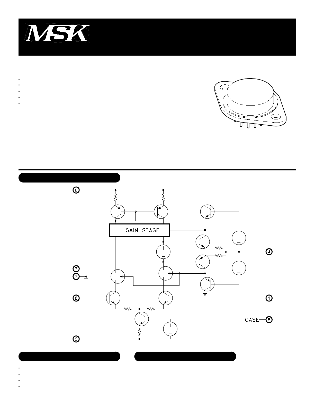
candidate for high speed systems. The circuit is packaged in a space efficient, hermetically sealed 8 pin TO-3 to
achieve good thermal efficiency and low cost. No isolation washer is necessary when heat sinking this device. The
MSK 690 is available in both industrial and military grades.
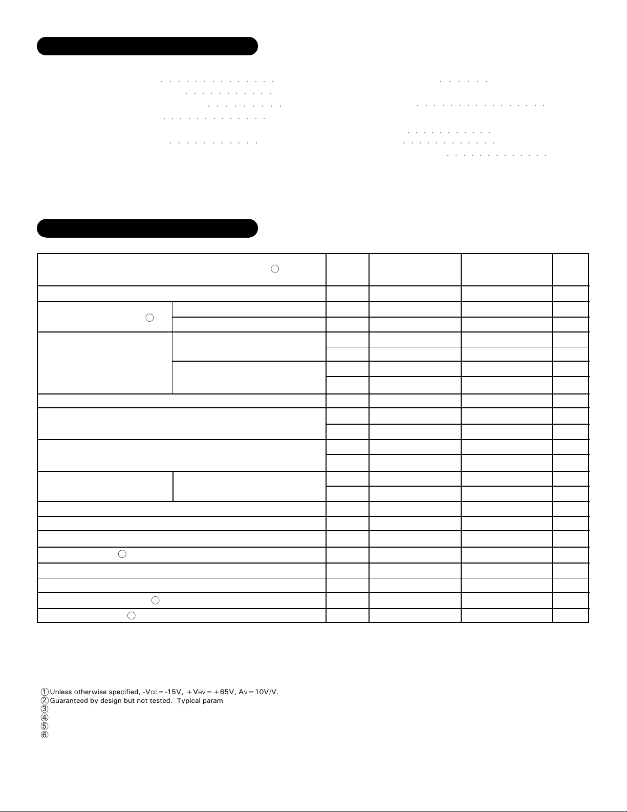
EQUIVALENT SCHEMATIC
TYPICAL APPLICATIONS
High Voltage Op-Amp
CRT Display Driver
High Voltage ATE Pin Driver
Level Shifter
PIN-OUT INFORMATION
Inverting Input
1
-VCC
2
Ground
3
Output
4
1
Non-Inverting Input
8
Ground
7
+VHV
6
Case Connection
5
Rev. A 8/00
Page 2
ABSOLUTE MAXIMUM RATINGS
-VCC
+VHV
VIND
IOUT
RθJC
Supply Voltage
○○○○○○○○○○○○○○
High Voltage Supply
Differential Input Voltage
Output Current
○○○○○○○○○○○○○
Thermal Resistance
(Output Devices)
○○○○○○○○○○○
ELECTRICAL SPECIFICATIONS
Parameter
STATIC
Supply Voltage Range
Quiescent Current
INPUT
Input Bias Current
Input Offset Current
Output Offset Voltage
OUTPUT
Output Voltage (High)
Output Voltage (Low)
Output Current
TRANSFER CHARACTERISTICS
Slew Rate
Open Loop Voltage Gain
Bandwidth (-3dB)
2
2
2
2
○○○○○○○○○○○
○○○○○○○○○
100mA
42°C/W
Test Conditions
-VCC
+VHV
-VCC=-15V
+VHV=+65V
VIN=0V
VIN=0V
VOUT=+50VDC Nominal
AV=100V/V
RL=10KΩ
RL=10KΩ
RL=10KΩ
f=1KHz
VO=24Vpp
-20V
+75V
15V
1
Storage Temperature
TST
Lead Temperature
TLD
(10 Seconds)
Case Operating Temperature
TC
(MSK690B)
(MSK690)
Junction Temperature
TJ
Group A
Subgroup
2,3
2,3
2,3
2,3
2,3
Min.
-12
-
+40
-
1
-
-
1
-
-
1
-
-
1
-
-
1
-
-
4
4
-
4
-
-
55
-
75
1200
55
20
○○○○○○○○○○○○○○○○
○○○○○○○○○○○
○○○○○○○○○○○○
MSK690B MSK690
Typ.
-15
+65
20
20
40
45
±50
±100
±50
±50
±0.1
±0.1
60
5.0
100
2000
65
35
○○○○○○
-65°C to +150°C
-55°C to +125°C
-40°C to +85°C
○○○○○○○○○○○○○
-12
55
75
55
20
Typ.
-15
+65
20
-
-
-
-
-
-
-
-
-
-
-
40
-
±50
-
±50
-
±0.1
-
60
5.0
-
100
2000
65
35
Max.
-18
+75
27
30
55
60
±195
±250
±100
±200
±0.7
±1.0
-
7.0
-
-
-
-
Min.
+40
1200
Max.
-18
+75
27
-
55
-
±250
-
±150
-
±0.7
-
-
7.0
-
-
-
-
300°C
150°C
Units
V
V
mA
mA
mA
mA
µA
µA
µA
µA
V
V
V
V
mA
V/µS
dB
MHz
NOTES:
1
Unless otherwise specified, -V
2
Guaranteed by design but not tested. Typical parameters are for reference only.
3
Industrial grade devices shall be tested to subgroups 1 and 4 unless otherwise requested.
4
Military grade devices ('B' suffix) shall be 100% tested to subgroups 1,2,3 and 4.
5
Subgroup 5 and 6 testing available upon request.
6
Subgroup 1,4 TC=+25°C
Subgroup 2,5 TC=+125°C
Subgroup 3,6 TA=-55°C
CC=-15V, +VHV=+65V, AV=10V/V.
Rev. A 8/002
Page 3

APPLICATION NOTES
ADJUSTABLE HIGH VOLTAGE POWER SUPPLY
The high voltage power supply of the MSK 690 can be ad-
justed from +40 volts to +75 volts. To minimize device power
dissipation, the +VHV power supply should be decreased as
much as possible without causing output signal clipping. The
following formula can be used to select a value for +VHV:
+VHV = VOUTMAX + 5.0V
This will ensure that the transistion times are not degraded due
to the output transistor temporarily going into saturation.
FEEDBACK CAPACITANCE
The gain range of the MSK 690 is ±5V/V to ±100V/V. When
configured for low closed loop gains in the range of ±5V/V to
±25V/V, a small 0.5pF to 2.0pF adjustable capacitor should
be placed in parallel with the feedback resistor. This capacitor
can be adjusted to tailor overshoot and minimize ringing de-
pending on the load. For closed loop gains greater than ±25V/
V the user may omit this capacitor without any loss in circuit
stability. See the table below labeled "recommended compo-
nent values" and the typical connection diagram for compo-
nent selection vs. closed loop gain.
CASE CONNECTION
The case of the MSK 690 is internally connected to pin five
of the package. This pin can be left as a no connect but it is
recommended that the user connect this pin to ground to re-
duce noise and improve overall circuit stability.
DECOUPLING AND LAYOUT
Since the MSK 690 is a high voltage amplifier, it is com-
monly used in high gain configurations. Consequently, any
noise introduced into the system through the power supplies
will be amplified by the system gain. It is therefore imperative
that proper power supply decoupling and printed circuit card
layout guidelines are adhered to. Each power supply should be
effectively decoupled with a parallel combination of capacitors
as shown in the Typical Inverting Connection Diagram. These
capacitors should be connected as close as possible to the pack-
age pins and lead lengths must be kept to a minimum. On the
printed circuit card, the input and output traces should be kept
apart whenever possible to avoid localized feedback. The power
supply lines should be kept as wide as possible to keep their
effective impedance down thereby minimizing pickup.
AV
-5V/V
-10V/V
-50V/V
-100V/V
RECOMMENDED COMPONENT VALUES
IN
-R
510Ω
270Ω
500Ω
500Ω
f
R
2.7KΩ
2.7KΩ
25KΩ
50KΩ
IN
+R
499Ω
249Ω
495Ω
499Ω
Cf
0.5-2.0pF
0.5-2.0pF
N/A
N/A
SOURCE RESISTOR SELECTION
When driving reactive loads, such as the effective capaci-
tance of a cathode ray tube, local oscillations may often occur
in the output transistors of the op-amp. To minimize these
oscillations, an output source resistor may be added in series
with the amplifier output and the capacitive load as seen in the
figure below. This R-C combination acts as a snubber network
that lowers the high frequency bandwidth. The source resistor
is typically in the 10 ohm to 100 ohm range. In exchange for
increased overall circuit stability, a minor reduction in amplifier
bandwidth may occur. The following formula may be used to
approximate the frequency at which the zero will occur on the
open loop plot due to the addition of the isolation resistor.
fZERO = 1/(2π(RISO + RO) CLOAD)
TYPICAL INVERTING CONNECTION DIAGRAM
SOURCE RESISTOR CONNECTION
3
Rev. A 8/00
Page 4

MECHANICAL SPECIFICATIONS
ALL DIMENSIONS ARE ±0.010 INCHES UNLESS OTHERWISE LABELED.
ORDERING INFORMATION
Part
Number
MSK690
MSK690B
Military-Mil-PRF-38534
M.S. Kennedy Corp.
4707 Dey Road, Liverpool, New York 13088
Phone (315) 701-6751
FAX (315) 701-6752
www.mskennedy.com
Screening Level
Industrial
The information contained herein is believed to be accurate at the time of printing. MSK reserves the right to make
changes to its products or specifications without notice, however, and assumes no liability for the use of its products.
4
Rev. A 8/00
 Loading...