

Page 1
M.S.KENNEDY CORP.
ISO 9001 CERTIFIED BY DSCC
WIDE BANDWIDTH,
VERY HIGH VOLTAGE
CRT VIDEO AMPLIFIER
643
4707 Dey Road Liverpool, N.Y. 13088
FEATURES:
Negative Output Voltage for Grid Drive
2.5nS Transition Times
Drives 8.5pF Capacitive Load With Ease
DC Coupled for Output Level Adjust
175MHz Bandwidth
75Vpp Output Swing
Replacement for CR3424R
MIL-PRF-38534 CERTIFIED
(315) 701-6751
DESCRIPTION:
The MSK 643(B) is a wide bandwidth, high voltage color or monochrome CRT video amplifier designed specifically
to drive the grid of today's most demanding high resolution CRT monitors. The MSK 643(B) is a transimpedance
amplifier capable of achieving a ±40V output voltage swing with an input current of ±10mA. The output of the
amplifier is DC biased at half the power supply voltage. Transition times in the range of 2.5nS enable the MSK 643
to drive 10nS pixels with ease and make it ideally suited for monitors with 1280 x 1024 or higher display resolutions.
The MSK 643 is mounted in a space efficient 9 pin single in-line bathtub package with two mounting tabs for direct
mounting to a heat sink or chassis.
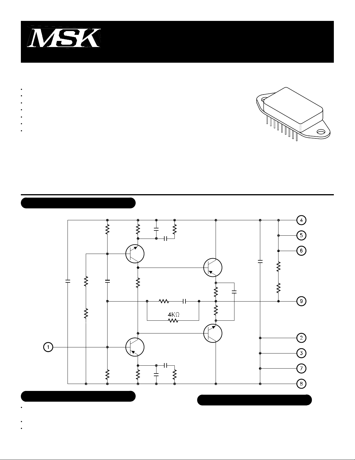
EQUIVALENT SCHEMATIC
TYPICAL APPLICATIONS
CRT Driver for Color and
Monochrome Monitors
High Voltage Transimpedance Amplifier
Ultra High Speed Amplifier for
Test Equipment
PIN-OUT INFORMATION
1
Inverting Input
2
Ground
3
Ground
4
-Vee
5
-Vee
1
6
-Vee
7
Ground
8
Ground
9
Output
Rev. B 12/01
Page 2
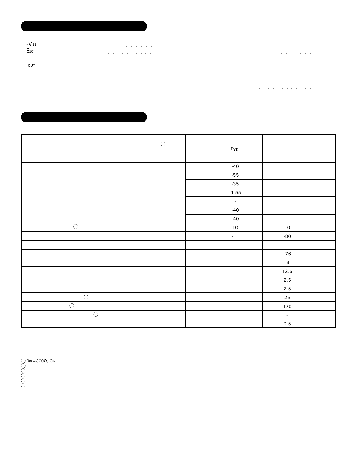
ABSOLUTE MAXIMUM RATINGS
-VEE
θJC
Supply Voltage
○○○○○○○○○○○○○○
Thermal Resistance
○○○○○○○○○○○
(Junction to Case)
IOUT
Peak Output Current
ELECTRICAL SPECIFICATIONS
Parameter
STATIC
Power Supply Current
Input Bias Voltage
Output Offset Voltage
Input Capacitance
Power Supply Range
DYNAMIC CHARACTERISTICS
Output Voltage High
Output Voltage Low
Voltage Gain
Rise Time
Fall Time
Overshoot (Adjustable)
-3dB Bandwidth
Low Frequency Tilt Voltage
Linearity Error
2
2
2
2
-100V
27°C/W
○○○○○○○○○○
Test Conditions
VIN=N/C
VIN=N/C
VIN=N/C
VIN=0.7V
Derated Performance
f=10KHz
f=10KHz
VIN=2VPP; f=10KHz
VOUT=40VPP
VOUT=40VPP
VOUT=20VPP
VOUT=20VPP
f=1KHz
f=10KHz; 5VPP≤VOUT≤50Vpp
250mA
1
TST
Storage Temperature Range
TLD
Lead Temperature Range
(10 Seconds)
TC
Case Operating Temperature
MSK643
MSK643B
TJ
Junction Temperature
○○○○○○○○○○○○
○○○○○○○○○○○
-Vee=-80V Unless Otherwise Specified
Min.
-
-
-
-1.4
-1.35
-38
-36
-
-60
-74
-
10.5
-
-
-
125
-
-
MSK 643B
Typ.
-40
-55
-35
-1.55
-
-40
-40
10
-80
-76
-4
12.5
2.5
2.5
25
175
-
0.5
Group A
Subgroup
1
2
3
1
2,3
1
2,3
-
-
4
4
4
4
4
-
-
-
4
-65°C to +150°C
○○○○○○○○○○
-55°C to +125°C
○○○○○○○○○○○○
MSK 643
Max.
-45
-65
-45
-1.7
-1.8
-42
-44
-100
14.5
3.4
3.4
1.5
Min.
-
-
-
-1.55
-1.3
-
-37
-
-
-
-60
-
-74
-6
-
10
-
-
-
-
-
120
-
5
-
300°C
-40°C to +85°C
175°C
-50
-43
-6
15
3.5
3.5
1.5
5
Units
mA
mA
-
mA
-
V
-
V
V
-
-
V
pF
V
-
V
V
V/V
nS
nS
%
-
MHz
-
V
%
Typ.
-40
-55
-35
-
-40
-
10
-80
-76
-4
12.5
2.5
2.5
25
175
-
0.5
Max.
-1.8
-100
NOTES:
1
RIN=300Ω, CIN=100pF, CLOAD=8.5pF, RL=∞, unless otherwise specified (See Figure 1).
2
Guaranteed by design but not tested. Typical parameters are representative of actual device performance but are for reference only.
3
Industrial grade devices shall be tested to subgroups 1 and 4 unless otherwise specified.
4
Military grade devices ('B' suffix) shall be 100% tested to subgroups 1,2,3 and 4.
5
Subgroup 5 and 6 testing available upon request.
6
Subgroup 1,4 TA=TC=+25°C
Subgroup 2,5 TA=TC=+125°C
Subgroup 3,6 TA=TC=-55°C
Rev. B 12/012
Page 3

APPLICATION NOTES
TYPICAL TEST CIRCUIT
The signal source in Figure 1 can be either a fast pulse gen-
erator or a network analyzer as long as the output impedance is
50 ohms. The DC level of the input should be -1.55V and all
cables should be kept as short as possible. Since total load
capacitance should be kept below 8.5pF, a FET probe should
be used on the ouput.
USING THE MSK 643
The output of the amplifier is biased at one half of the power
supply voltage. An output voltage swing of ±35 volts is typi-
cal with a power supply voltage of -80 volts. With an 8.5pF
capacitive load, transistion times are in the 2.5nS range. If a
spark gap current limiting resistor is used on the output of the
amplifier and the transistion times are degraded, a peaking coil
may be used to preserve system performance. The optimum
value for this coil will be in the range of 100 to 200nH and can
best be determined by trial and error. The output of the MSK
643 is not short circuit protected, therefore, purely resistive
loads should be no less than 800 ohms at any time to avoid
damaging the output.
OPERATION CONSIDERATIONS
The input of the MSK 643 rests at a -1.55VDC level with the
input terminal open. In this state, the output rests at one half
of the power supply voltage. When connecting a pulse genera-
tor to the input of the amplifier, the DC level should be offset
so that the signal is centered around -1.55V. During character-
ization, the input should be coupled to the MSK 643 through a
parallel combination of a variable resistor and variable capacitor
peaking circuit. Optimum values for the peaking circuit can be
determined experimentally. The optimum value of load capaci-
tance is 8.5pF. Viewing the output with a normal oscilloscope
probe would seriously degrade performance. A FET probe fit-
ted with a 100:1 voltage divider will add only approximately
1.5pF of capacitance to the load and is highly recommended.
An experimental circuit along with recommended values can be
found in Figure 2.
OUTPUT ISSUES
The output of the MSK 643 is a pair of bipolar emitter follow-
ers configured in a complimentary push pull configuration. This
configuration eliminates the need for a pull up load resistor and
makes the amplifier less susceptible to load capacitance varia-
tions. Connecting a wire or cable from the output of the ampli-
fier to the CRT grid can create a resonant circuit which can
cause unwanted oscillations or overshoot at its resonant fre-
quency. A damping resistor in series with the lead inductance
will alleviate this condition. The optimum value of this resistor
can be determined using the following formula:
R = 2* √L/C
This resistor also doubles as an arcing protector. In the bread-
boarding stage, the value of this resistor should be determined
experimentally. Resistance in the range of 50 to 100 ohms is
usually sufficient. If a quick, simple peaking network is de-
sired, a 300 ohm cable terminated by a capacitor will act like an
inductor in the frequency range involved.
TRANSIMPEDANCE AMPLIFICATION
Transimpedance amplifiers relate input current to output volt-
age. The MSK 643 contains an internal 4KΩ feedback resistor.
This resistor converts input current to output voltage in the
following manner (See Figure 1):
±1.43V (referenced to -1.55Vdc) across the 300Ω input
resistor results in an input current of ±4.77mA. This current
flows through the 4KΩ feedback resistor and results approxi-
mately in a ±20V swing at the output. The actual voltage gain
of the typical MSK 643 circuit may be slightly less due to tran-
sistor losses. The following formula approximates voltage gain
including potential losses:
Voltage Gain (V/V) = 4KΩ/(Rin + L) L ≈ 25Ω
HEAT SINKING
The MSK 643 requires heat sinking in most applications. The
following formula may be applied to determine if a heat sink is
necessary and what size and type to use.
Rθsa = ((Tj-Ta)/Pd ) - (Rθjc) - (Rθcs)
WHERE
Tj = Junction Temperature
Pd = Total power dissipation
Rθjc = Junction to case thermal resistance
Rθcs = Case to heat sink thermal resistance
Rθsa = Heat sink to ambient thermal resistance
Tc = Case temperature
Ta = Ambient temperature
Ts = Sink temperature
EXAMPLE
Tj = 150°C
Ta = 100°C
Pd = 1.5W
Rθjc = 27°C/W
Rθcs = 0.15°C/W
Solving the above equation for Rθsa (heat sink thermal conduc-
tivity) shows that the heat sink for this application must have a
thermal resistance of no more than 6.0°C/W to maintain a junc-
tion temperature of no more than 150°C.
3
Rev. B 12/01
Page 4

TYPICAL PERFORMANCE CURVES
4
Rev. B 12/01
Page 5

COMPLETE VIDEO SYSTEM
Figure 3 above illustrates how an MSK 620 and MSK 643 can be used to build a compete video system for high voltage grid
drive. RA and RB act as a level shift stage to match the +3.9Vdc level at the output of the MSK 620 with the -1.55Vdc level at
the input of the MSK 643. The output of the MSK 643 is sampled and fed back to the MSK 620. This scheme provides black level
control superior to sampling the signal at pin 14 of the MSK 620. The general rule of thumb for transition times for a video driver
is that rising and falling edges should be no more than one third the pixel time of the monitor. To improve rise and fall time in the
system, the peaking capacitor Cp was added across the input resistor of the MSK 643. At high frequencies Cp increases the gain
of the amplifier there by causing peaking. Cp should be a variable capacitor so that the response of the amplifier can be fine tuned
for minimum transition time with minimum overshoot.
Rev. B 12/015
Page 6

MECHANICAL SPECIFICATIONS
NOTE: ESD Triangle indicates Pin 1.
ALL DIMENSIONS ARE ±0.010 INCHES UNLESS OTHERWISE LABELED
ORDERING INFORMATION
Part
Number
MSK643
MSK643B
M.S. Kennedy Corp.
4707 Dey Road, Liverpool, New York 13088
Screening Level
Industrial
Military-Mil-PRF-38534
Phone (315) 701-6751
FAX (315) 701-6752
www.mskennedy.com
The information contained herein is believed to be accurate at the time of printing. MSK reserves the right to make
changes to its products or specifications without notice, however, and assumes no liability for the use of its products.
Rev. B 12/016
 Loading...