

Page 1
M.S.KENNEDY CORP.
ISO-9001 CERTIFIED BY DSCC
HIGH CURRENT,
SUPER LOW DROPOUT
ADJUSTABLE VOLTAGE REGULATOR
5021
4707 Dey Road Liverpool, N.Y. 13088
FEATURES:
Extremely Low Dropout Voltage: 0.50V @ 20 Amps
Output Voltage Adjustable from 1.3V to 36V with Two External Resistors
TTL Level Enable Pin
Externally Programmable Current Limit
Low Quiescent Current
Available Fully Qualified to Mil-PRF-38534
Output Current to 20 Amps
Regulation Dropout Fault Pin
MIL-PRF-38534 CERTIFIED
(315) 701-6751
DESCRIPTION:
The MSK 5021 is a user adjustable voltage regulator capable of delivering 20 amps to a load with only a 0.5 volt
dropout voltage rating. The output voltage is adjustable from 1.3 volts to 36 volts through the selection of two
external resistors. Low dropout voltage ratings are achieved by employing a unique parallel MOSFET output pass
transistor configuration which drives power dissipation down and efficiency up. Accuracy is guaranteed with a ±1%
voltage tolerance at room temperature that only varies ±2% over temperature. A TTL level can be used to enable/
disable the device and a regulation dropout fault pin provides a means of monitoring the output level. The MSK 5021
is packaged in a thermally efficient 12 pin power dip that can be bolted directly to a heat sink.
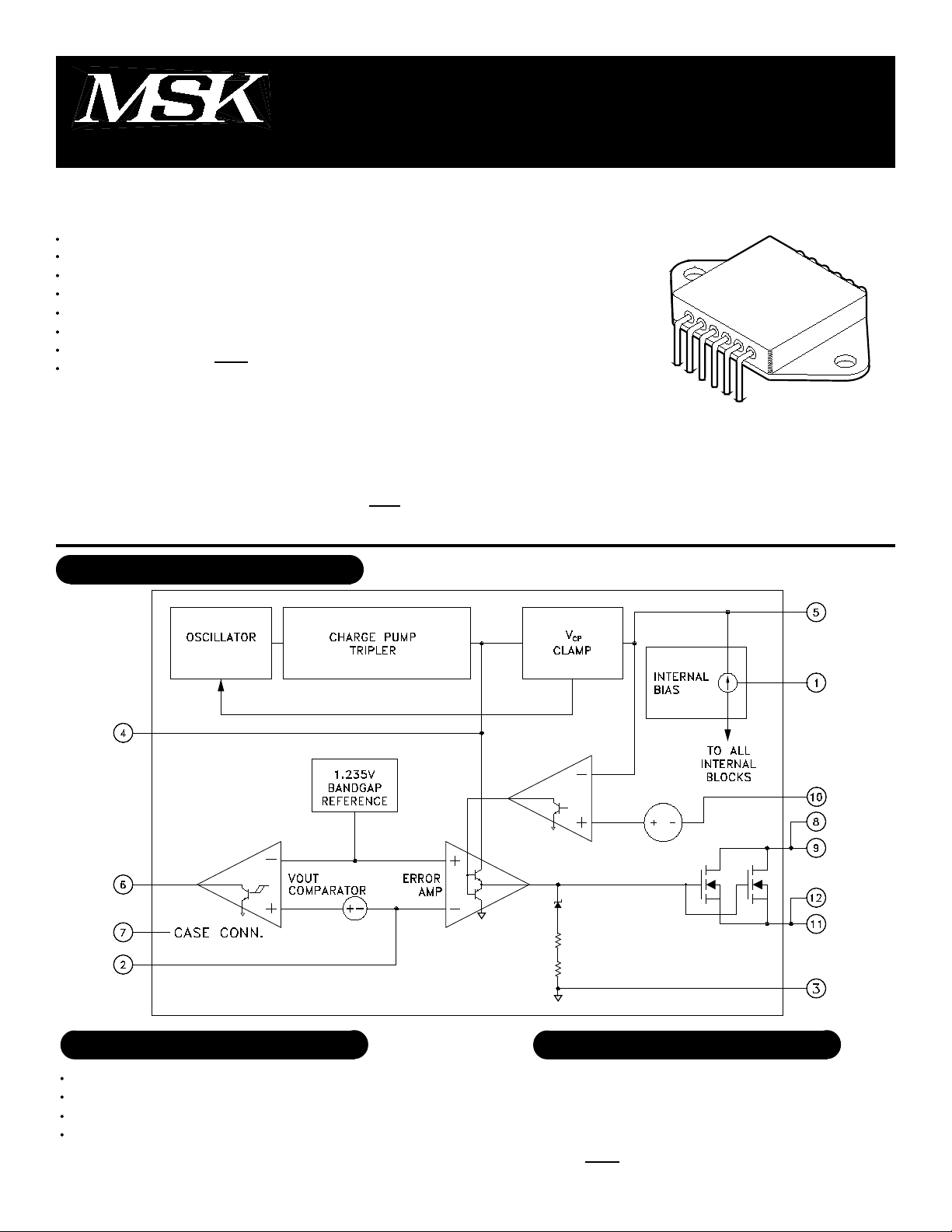
EQUIVALENT SCHEMATIC
TYPICAL APPLICATIONS
High Efficiency, High Current Linear Regulators
Adjustable Voltage/Current Regulators
System Power Supplies
Switching Power Supply Post Regulators
PIN-OUT INFORMATION
12
1
Enable
2
VAdjust
3
Ground
4
CPump
5
Input
6
Fault
1
Output
11
Output
10
Sense
9
VSC
8
VSC
7
Case Connection
Rev. B 7/00
Page 2
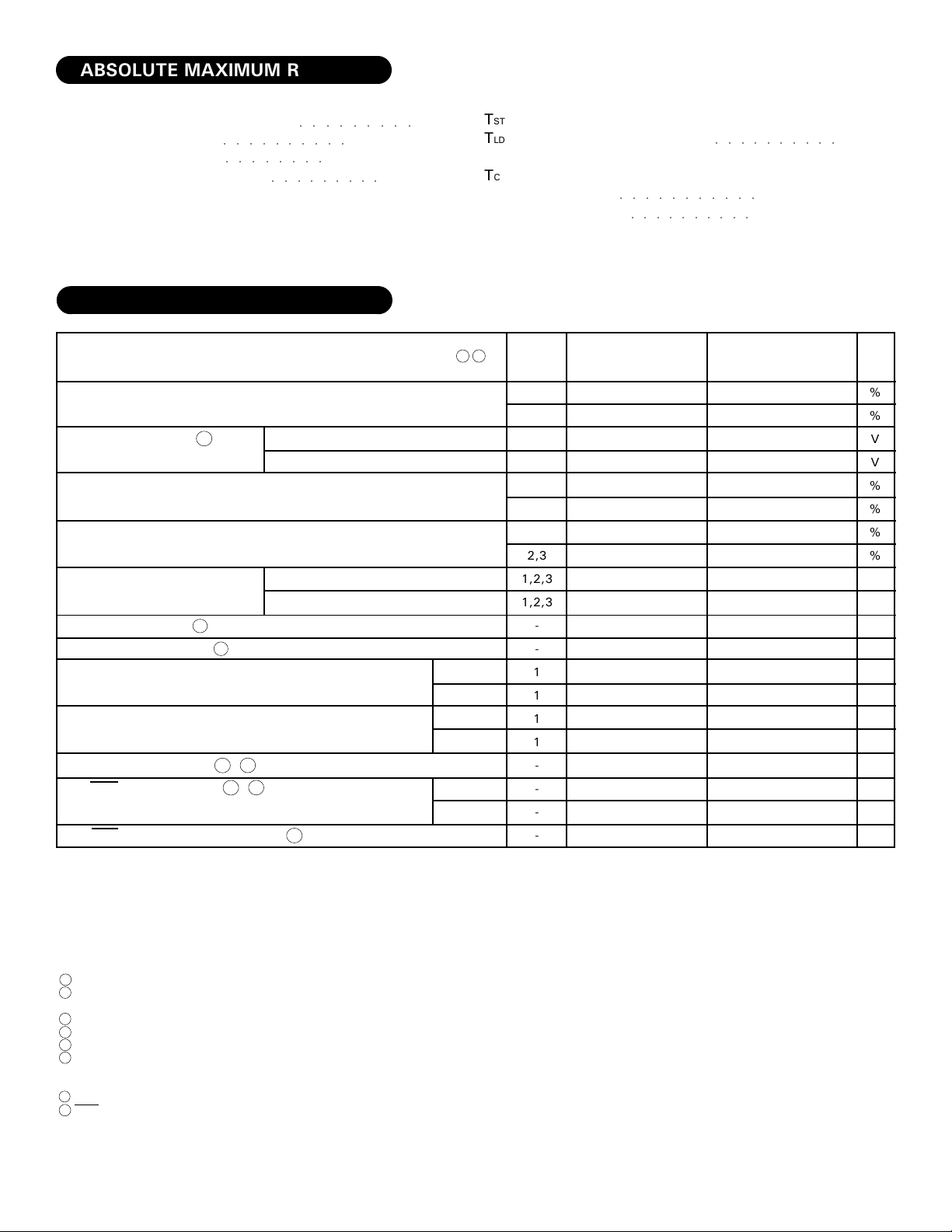
ABSOLUTE MAXIMUM RATINGS
Input Voltage (WRT VOUT)
VIN
Enable Voltage
VEN
Output Current
IOUT
Junction Temperature
TJ
○○○○○○○○○○
○○○○○○○○
○○○○○○○○○
20A within SOA
○○○○○○○○○
ELECTRICAL SPECIFICATIONS
36V
-0.3V to 36V
+175°C
TST
Storage Temperature Range
TLD
Lead Temperature Range
(10 Seconds)
TC
Case Operating Temperature
MSK5021
MSK5021B
○○○○○○○○○○○
○○○○○○○○○○
-65°C to +150°C
○○○○○○○○○○
-40°C to +85°C
-55°C to +125°C
300°C
Parameter
Output Voltage Tolerance
Dropout Voltage
2
Load Regulation
Line Regulation
Quiescent Current
Ripple Rejection 2
Thermal Resistance 2
Enable Input Voltage
Enable Input Current
2
Output Settling Time
Fault Output Voltage
7
2 8
Fault Output Sink Current Range
Test Conditions
1
IOUT=0A; VIN=VOUT+3V
IOUT= 0A
IOUT=20A
VIN=VOUT+3V
0A ≤ IOUT ≤ 20A
(VOUT +1.5V) ≤ VIN ≤ (VOUT+15V)
IOUT=0A
VEN=5V; VIN=VOUT+3V; IOUT=0A
VEN=0V; VIN=VOUT+3V; IOUT=0A
f=120Hz
Junction to Case
HIGH
LOW
HIGH
LOW
To within 10mV (IOUT=0A)
IFAULT=1mA
HIGH
LOW
2
3
Group A
Subgroup
1
2,3
1
1
1
2,3
1
2,3
1,2,3
1,2,3
-
-
1
1
1
1
-
-
-
-
MSK 5021(B)
Min.
Typ.
-
±0.5
-
±1.0
-
0.002
-
0.50
-
±0.5
-
±0.5
-
±0.5
-
±0.5
-
-
-
-
2.4
-
-
-
-
-
-
0.09
1
20
10
45
0.5
1.2
1.2
20
10
0.5
VIN
MSK 5021
2.4
1
Typ.
±0.5
-
-
-
-
-
-
-
-
-
-
-
-
-
0.002
0.5
±0.5
-
±0.5
-
20
10
45
0.5
1.2
1.2
-
20
-
10
-
0.5
-
VIN
-
0.09
-
-
Max.
Min.
±1.0
±2.0
0.010
0.75
±1.0
±2.0
±1.0
±1.0
30
50
-
0.6
-
0.8
50
25
-
-
-
10
-
Max.
±1.0
-
0.010
1.0
±1.0
-
±1.0
-
30
50
-
0.6
-
0.8
50
25
-
-
-
10
Units
%
%
V
V
%
%
%
%
mA
µA
dB
°C/W
V
V
µA
µA
mS
V
V
mA
NOTES:
Output decoupled to ground using 33µF minimum capacitor and RSC=0Ω unless otherwise specified.
1
This parameter is guaranteed by design but need not be tested. Typical parameters are representative of
2
actual device performance but are for reference only.
All output parameters are tested using a low duty cycle pulse to maintain TJ = TC.
3
Industrial grade devices shall be tested to subgroup 1 only unless otherwise specified.
4
Military grade devices ('B' suffix) shall be 100% tested to subgroups 1,2 and 3.
5
Subgroup 1
6
Subgroup 2
Subgroup 3
After application of enable pulse.
7
Fault pin connected to VIN through a 5.1KΩ resistor for VIN=5.0V.
8
TA=TC=+25°C
TA=TC=+125°C
TC=TC=-55°C
2
Rev. B 7/00
Page 3

APPLICATION NOTES
MINIMIZING OUTPUT RIPPLE:
The output voltage ripple of the MSK 5021 voltage regulator
can be minimized by placing a filter capacitor from the output
to ground. The optimum value for this capacitor may vary
from one application to the next and is best determined by
experimentation. Transient load response can also be improved
by placing a 33uF or larger capacitor directly across the load.
CASE CONNECTIONS:
The case of the MSK 5021 is connected to pin seven of the
package but isolated from the internal circuitry allowing direct
attachment of the heat sink to the case. It may be necessary
in some applications to ground the case to limit noise or elimi-
nate oscillations on the output. Pin seven can be left as a no
connect if the designer chooses.
LOAD REGULATION:
For best results, the ground pin should be connected directly to
the load (see next note). This effectively reduces the ground
loop effect and eliminates excessive voltage drop in the sense
leg. It is also important to keep the output connection be-
tween the regulator and the load as short as possible since this
directly affects the load regulation. For example, if 20 gauge
wire were used which has a resistance of about .008 ohms per
foot, this would result in a drop of 80mV/ft at a load current of
10 amps.
LOAD CONNECTIONS:
In voltage regulator applications where very large load cur-
rents are present, the load connection is very important. The
path connecting the output of the regulator to the load must be
extremely low impedance to avoid affecting the load regulation
specifications. Any impedance in this path will form a voltage
divider with the load. The same holds true for the connection
from the low end of the load to ground. For best load regula-
tion, the low end of the load must be connected directly to pin
3 of the MSK 5021 and not to a ground plane inches away
from the hybrid.
ENABLE/DISABLE PIN:
The MSK 5021 voltage regulator is equipped with a TTL com-
patible ENABLE pin. A TTL high level on this pin activates the
internal bias circuit and powers up the device. A TTL low level
on this pin places the controller in shutdown mode and the
device draws only 10µA of quiescent current. This pin can be
pulled up to VIN if the enable function is not desired.
FAULT PIN CONNECTIONS:
Pin 6 of the MSK 5021 is the FAULT pin. When the output
voltage drops 6% or more below its nominal value, the voltage
level on the fault pin drops to a logic low (typically less than
0.1 volts). This pin can be used to drive a light emitting diode
or other external circuitry as long as the current is limited to
less than 10.0mA (see typical connection diagram). The fault
pin is an open collector output so the high state output voltage
will be equal to the pull up voltage since no current flows under
these conditions.
CPUMP:
For all applications, the user must connect a 1.0uF capacitor
from pin 4 directly to ground. This capacitor is part of the
circuit which drives the gate of the internal MOSFETS. Ap-
proximately three times the voltage seen on the input will ap-
pear across this capacitor. Careful attention must be paid to
capacitor voltage rating since voltages larger than the power
supply are present.
HEAT SINK SELECTION:
To select a heat sink for the MSK 5021, the following formula
for convective heat flow must be used.
Governing Equation:
Tj = Pd x (Rθjc + Rθcs + Rθsa) + Ta
WHERE:
Tj = Junction Temperature
Pd = Total Power Dissipation
Rθjc = Junction to Case Thermal Resistance
Rθcs = Case to Heat Sink Thermal Resistance
Rθsa = Heat Sink to Ambient Thermal Resistance
Ta = Ambient Temperature
First, the power dissipation must be calculated as follows:
Power Dissipation = (Vin - Vout) x Iout
Next, the user must select a maximum junction temperature.
The absolute maximum allowable junction temperature is 175°C.
The equation may now be rearranged to solve for the required
heat sink to ambient thermal resistance (R
EXAMPLE;
An MSK 5021 is configured for Vin = +7V and Vout = +3.3V.
Iout is a continuous 10A DC level. The ambient temperature is
+25°C. The maximum desired junction temperature is 150°C.
Rθjc = 0.5°C/W and Rθcs = 0.15°C/W typically.
Power Dissipation = (7V - 3.3V) x (10A)
= 37 Watts
Solve for Rθsa:
Rθsa = 150°C - 25°C - 0.5°C/W - 0.15°C/W
37W
= 2.728°C/W
In this example, a heat sink with a thermal resistance of no
more than 2.73°C/W must be used to maintain a junction tem-
perature of no more than 150°C.
θsa).
POWER DISSIPATION:
The output pass transistors in the MSK 5021 are rated to dissi-
pate nearly 200 watts. The limiting factor of this device is
effective dissipation of heat generated under such conditions.
For example, to dissipate 200 watts, calculations show that
the MSK 5021 would have to be bolted to the underbelly of a
submarine submerged in the Artic Ocean! Careful consider-
ation must be paid to heat dissipation and junction temperature
when applying this device.
CURRENT LIMIT CONNECTIONS:
To implement current limiting, a sense resistor (Rsc) must be
placed from pin 5 to pins 8 and 9 as shown in the typical
connection diagram. When the voltage drop across the sense
resistor reaches 35mV, the internal control loop limits the out-
put current only enough to maintain 35mV across the sense
resistor. The device is not disabled. The following formula
may be used to find the correct value of sense resistance:
RSC=35mV/ILIM
If current limit is not required simply connect the Vsc pins di-
rectly to the input voltage along with the sense pin. Refer to
the typical connection diagram for an illustration.
3
Rev. B 7/00
Page 4

TYPICAL PERFORMANCE CURVES
4
Rev. B 7/00
Page 5

TYPICAL CONNECTION DIAGRAM
The above connection diagram illustrates an MSK 5021 regulator. Q1 turns on the fault L.E.D. when pin 6 of the
hybrid drops to a logic low. Current into pin 6 is limited to approximately 1mA by the 12KΩ resistor from pin 5 to pin
6. The optimum value of capacitance COUT may vary from one application to the next depending on the load applied.
10µF is a good starting point. The ENABLE input is TTL compatible but can be tied to the input voltage when
shutdown is not needed. RSC should be selected for the desired current limit. See current limit connections applica-
tion note.
OUTPUT VOLTAGE ADJUSTMENT:
The output voltage of the MSK 5021 can be adjusted from +1.3 volts to +36 volts. Refer to the following
formula for resistor divider selection. R2 shall be 10KΩ for all applications.
RADJUST = 1 x 10 ((Vout/1.235)-1)
4
Rev. B 7/005
Page 6

MECHANICAL SPECIFICATIONS
ESD Triangle indicates Pin 1.
NOTE: ALL DIMENSIONS ARE ±0.010 INCHES UNLESS OTHERWISE LABELED.
ORDERING INFORMATION
Part
Number
MSK5021
MSK5021B
Screening Level
Industrial
Military-Mil-PRF-38534
M.S. Kennedy Corp.
4707 Dey Road, Liverpool, New York 13088
Phone (315) 701-6751
FAX (315) 701-6752
www.mskennedy.com
The information contained herein is believed to be accurate at the time of printing. MSK reserves the right to make
changes to its products or specifications without notice, however, and assumes no liability for the use of its products.
Rev. B 7/006
 Loading...