

Page 1
ISO 9001 CERTIFIED BY DSCC
10 AMP, 75V, 3 PHASE MOSFET
BRIDGE WITH INTELLIGENT
M.S.KENNEDY CORP.
4707 Dey Road Liverpool, M/Y. 13088 (315) 701-6751
INTEGRATED GATE DRIVE
FEATURES:
75 Volt Motor Supply Voltage
10 Amp Output Switch Capability, All N-Channel MOSFET Output Bridge
100% Duty Cycle High Side Conduction Capable
Suitable for PWM Applications from DC to 100KHz
Shoot-Through/Cross Conduction Protection
Undervoltage Lockout Protection
Programmable Dead-Time Control
Low Active Enable for Bridge Shutdown Control
Isolated Base Plate Design for High Voltage Isolation Plus Good Thermal Transfer
DESCRIPTION:
The MSK 4400 is a 3 phase MOSFET bridge plus drivers in a convenient isolated baseplate package. The
module is capable of 10 amps of output current and 75 volts of DC bus voltage. It has a full line of protection features,
including undervoltage lockout protection of the bias voltage, cross conduction control and a user programmable dead-time
control for shoot-through elimination. In addition, the bridge may be shut down by using the ENABLE control. The MSK
4400 provides good thermal conductivity for the MOSFETs due to an isolated plate design that allows direct heat sinking of
the device without insulators.
4400
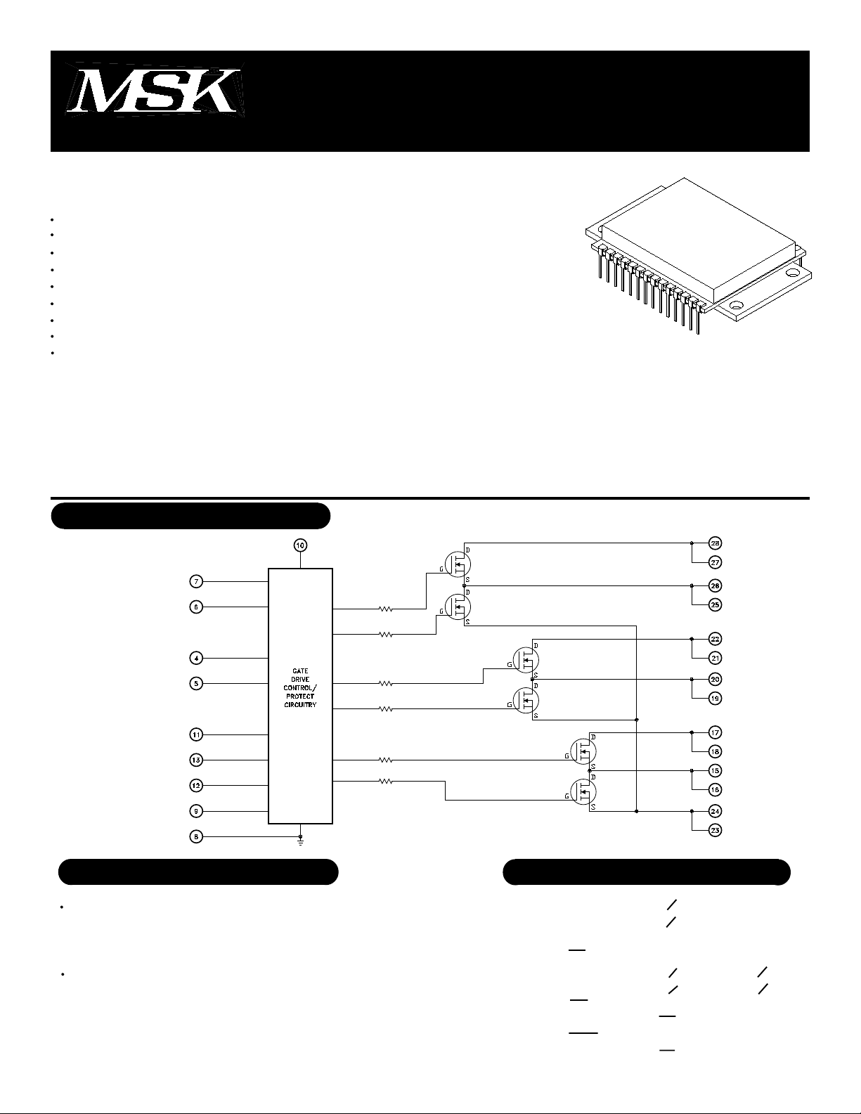
EQUIVALENT SCHEMATIC
TYPICAL APPLICATIONS
3 Phase Brushless DC
Servo Control
Fin Actuator Control
Gimbal Control
3 Phase AC
Induction Motor Control
HVAC Blower Control
PIN-OUT INFORMATION
N/C
1
N/C
2
N/C
3
BH
4
BL
5
AL
6
AH
7
GND
8
SWR
9
VBIAS
1
10
20
19
18
17
16
15
14
13
12
11
BO
BO
CV+
CV+
CO
CO
N/C
CH
CL
EN
AV+
28
AV+
27
AO
26
AO
25
RSENSE
24
RSENSE
23
BV+
22
BV+
21
Rev. E 6/01
Page 2
ABSOLUTE MAXIMUM RATINGS
High Voltage Supply
V+
Bias Supply
VBIAS
Logic Input Voltages
VIND
Continuous Output Current
IOUT
Peak Output Current
IPK
○○○○○○○○○○○○○○○○○○○○
○○○○○○○○○○○○○○○
○○○○
○○○○○○○○○○○○○○○
-0.3V to VBIAS +0.3V
○○○○○○○○○○○
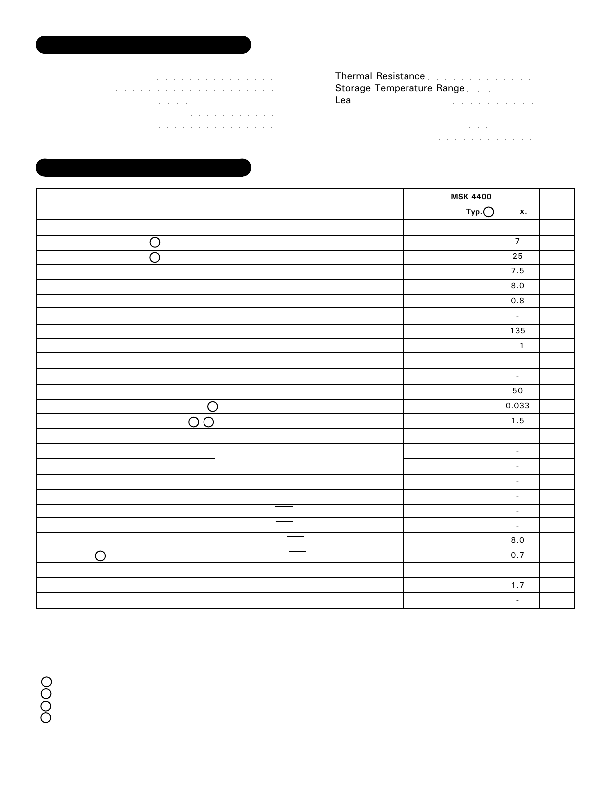
ELECTRICAL SPECIFICATIONS
Parameter
CONTROL SECTION
VBIAS Quiescent Current 4
VBIAS Operating Current 4
Undervoltage Threshold (Falling)
Undervoltage Threshold (Rising)
Low Level Input Voltage
High Level Input Voltage
Low Level Input Current
High Level Input Current
OUTPUT BRIDGE
Drain-Source Breakdown Voltage
Drain-Source Leakage Current
Drain-Source On Resistance (Each FET) 1
Voltage Drop Across Bridge Phase 2 4
SWITCHING CHARACTERISTICS
Rise Time
Fall Time
Enable Turn-On Prop Delay (Lower)
Enable Turn-Off Prop Delay (Lower)
Enable Turn-On Prop Delay (Upper)
Enable Turn-Off Prop Delay (Upper)
Dead Time
Dead Time 4
SOURCE-DRAIN DIODE CHARACTERISTICS
Forward Voltage
Reverse Recovery Time
75V
16V
10A
25A
Test Condition
@ 25°C unless otherwise specified
All Inputs Off
f=20KHz, 50% Duty Cycle
VIN=0V
VIN=5V
ID=100µA, All Inputs Off
VDS=70V
ID=25A
ID=10A
V+=38V
ID=25A Peak
SWR Resistor=∞
SWR Resistor=∞
SWR=Open
SWR=12K
ISD=10A
ISD=10A, di/dt=100A/µS
Thermal Resistance
θJC
Storage Temperature Range
TST
Lead Temperature Range
TLD
(10 Seconds)
Case Operating Temperature
TC
Junction Temperature
TJ
○○○○○○○○○○○○○
-55°C to +150°C
○○○
○○○○○○○○○○
-40°C to +125°C
○○○
○○○○○○○○○○○○
MSK 4400
Min.
-
-
5.75
6.2
-
2.7
60
-1
75
-
-
-
-
-
-
-
-
-
6.0
0.3
-
-
Typ. 3
6
22
6.6
7.1
-
-
100
-
-
-
-
1.3
62
58
100
100
2
2
7.0
0.5
-
120
Max.
135
0.033
7
25
7.5
8.0
0.8
-
+1
-
50
1.5
-
-
-
-
-
-
8.0
0.7
1.7
-
3.9 C/W
+300°C
+150°C
Units
mAmp
mAmp
Volts
Volts
Volts
Volts
µAmp
µAmp
V
µAmp
Ω
VOLTS
nSec
nSec
µSec
µSec
µSec
µSec
µSec
µSec
Volts
nSec
NOTES:
1 Use for maximum MOSFET junction temperature calculations.
2 Use for overall efficiency and dissipation calculations.
3 Typical parameters are representative of actual device performance but are for reference only.
4 Parameter is 100% tested on production devices. All other parameters are guaranteed.
2
Rev.E 6/01
Page 3

APPLICATION NOTES
MSK 4400 PINOUT DESCRIPTIONS
AØ, BØ, CØ - Are the connections to the motor phase
windings from the bridge output. The wiring to these pins
should be sized according to the required current by the
motor. There are no short circuit provisions for these out-
puts. Shorts to V+ or gound from these pins must be
avoided or the bridge will be destroyed.
AL, BL, CL - Are the logic level inputs for controlling the
low side switch for each of the three phases. A logic
HIGH turns the low side output on, sinking the output cur-
rent and pulling it down. If the corresponding high side
switch is ON, the device will turn off the high side output,
insert the dead time and then command the lowside out-
put on. The low side input has priority over the high side
input.
AH, BH, CH - Are the logic level inputs for controlling the
high side switch for each of the three phases. A logic low
turns the high side output ON, sourcing the output current
and pulling it up. If the corresponding low side switch is
ON, the device will ignore the high side input until the
lowside is turned off and dead time has elapsed. Again,
the lowside input has priority.
EN - Is the logic level input for enabling and disabling the
bridge outputs. A logic low enables output switching.
GND - Is the logic input return connection, the VBIAS
return and the V+ return.
SWR - Is the control for the amount of dead time be-
tween a high side switch ON and the corresponding low
side switch OFF and vice versa. Leaving it open creates
the most dead time, while connecting a 12 K resistor to
VBIAS creates the least.
VBIAS - Is the supply voltage for running all of the low
level logic and gate drive functions.This pin should be by-
passed to GND using a 0.1µF ceramic capacitor and a
4.7µF bulk capacitor.
AV+,BV+,CV+ - Are the power connections from the
hybrid to the bus. The pins for each phase are brought out
separately and must be connected together to the V+
source externally. The external wiring to these pins should
be sized according to the RMS current required by the
motor. These pins should be bypassed by a high quality
monolithic ceramic capacitor for high frequencies and
enough bulk capacitance for keeping the V+supply from
drooping. 1000µF of bulk capacitance was used in the
test circuit. The voltage range on these pins is from 16
volts up to 75 volts.
RSENSE - Is the connection point for the bottom of the
three phase bridge. A low value resistor between here
and the GND will produce a voltage proportional to cur-
rent in the bridge. Both pins must be connected. If a resis-
tor is not used, these pins must be connected to GND.
3
Rev. E 6/01
Page 4

TYPICAL APPLICATION SCHEMATIC
OPEN LOOP BRUSHLESS DC MOTOR SPEED CONTROL
TYPICAL PERFORMANCE CURVES
4
Rev. E 6/01
Page 5

MECHANICAL SPECIFICATIONS
NOTE: ALL DIMENSIONS ARE ±0.010 INCHES UNLESS OTHERWISE LABELED.
ORDERING INFORMATION
Part
Number
MSK4400S
MSK4400D
Straight
Down
MSK4400U
4707 Dey Road, Liverpool, N.Y. 13088
The information contained herein is believed to be accurate at the time of printing. MSK reserves the right to make
changes to its products or specifications without notice, however, and assumes no liability for the use of its products.
Please visit our websit for the most recent revision of this datasheet.
Lead
Screening Level
Option
Industrial
Industrial
Up
Industrial
M.S. Kennedy Corp.
Phone (315) 701-6751
FAX (315) 701-6752
www.mskennedy.com
5
Rev. E 6/01
 Loading...