

Page 1
M.S.KENNEDY CORP.
ISO-9001 CERTIFIED BY DSCC
28 AMP, 500 VOLT IGBT PLUS DIODE
SMART POWER 3-PHASE MOTOR
DRIVE POWER HYBRID
4357
4707 Dey Road Liverpool, N.Y. 13088
FEATURES:
500V, 28 Amp Capability at 125°C
Ultra Low Thermal Resistance
Integral Free Wheeling Fast Recovery Epitaxial Diode (FRED)
Self-Contained, Smart Lowside/Highside Drive Circuitry
Under-Voltage Lockout, Internal 2uS Deadtime
Capable of Switching Frequencies to 25KHz
Isolated Case Allows Direct Heat Sinking
Case Bolt-down Design Allows Superior Heat Dissipation
MIL-PRF-38534 CERTIFIED
(315) 701-6751
DESCRIPTION:
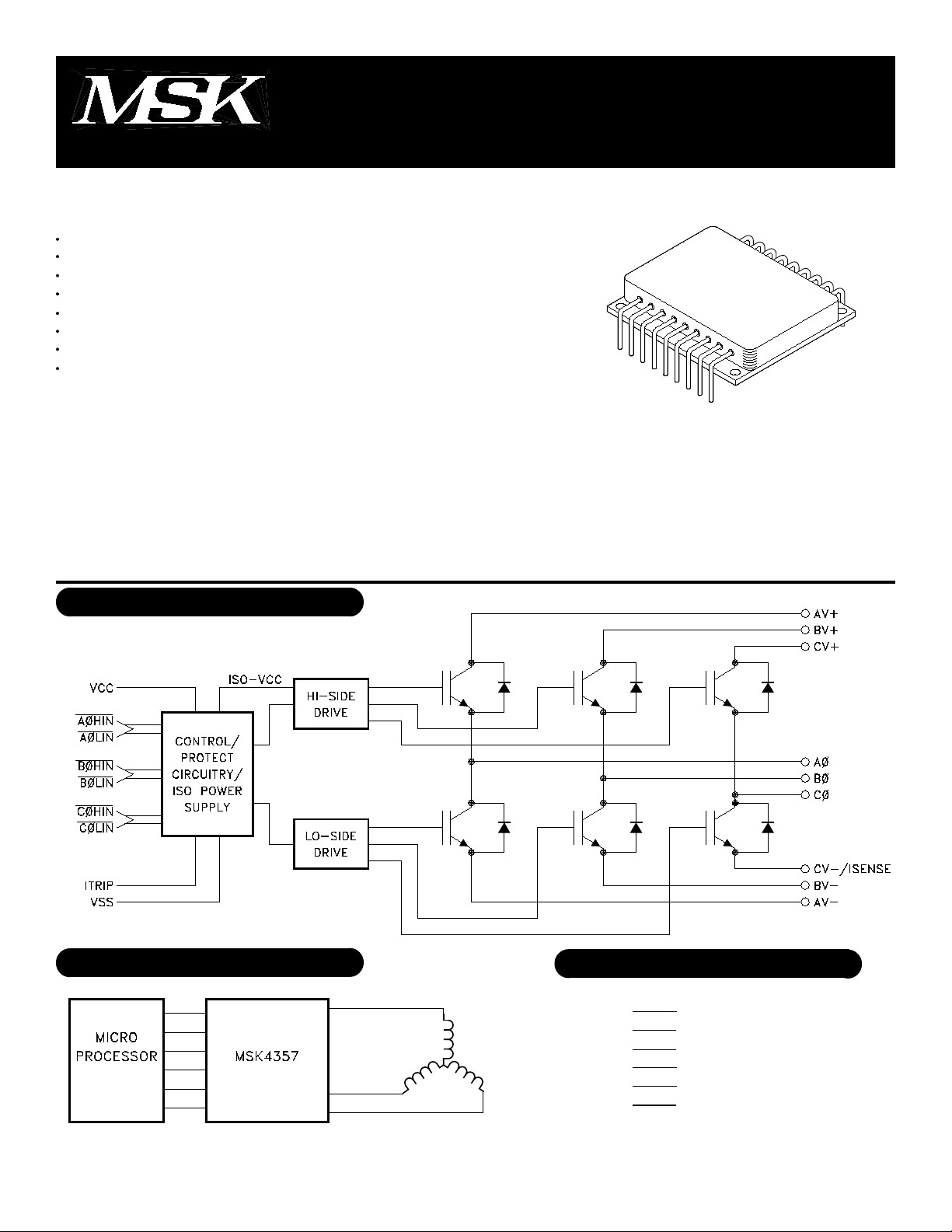
The MSK 4357 is a 28 Amp, 3 Phase Bridge Smart Power Motor Drive Hybrid with a 500 volt rating. The output
switches are Insulated Gate Bipolar Transistors (IGBT's) tailored for high switching speeds. The free-wheeling diodes
are the new Fast Recovery Epitaxial Diodes (FRED's) to provide matched current capabilities with the IGBT's and are
specified with excellent reverse recovery times at high current ratings. This new smart power motor drive hybrid is
compatible with 5v CMOS or TTL logic levels. The internal circuitry prevents simultaneous turn-on of the in-line half
bridge transistors with a built-in 2uS deadtime to prevent shoot-through. Undervoltage lockout shuts down the bridge
when the supply voltage gets to a point of incomplete turn-on of the output switches. The internal high-side power
supply derived from the +15 volt supply completely eliminates the need for 3 floating independent power supplies for
the high-side drive.
EQUIVALENT SCHEMATIC
TYPICAL APPLICATIONS
3 PHASE SIX STEP DC BRUSHLESS MOTOR DRIVE
OR 3 PHASE SINUSOIDAL INDUCTION MOTOR DRIVE
PIN-OUT INFORMATION
1
VCC
2
AØHIN
3
AØLIN
4
BØHIN
5
BØLIN
6
CØHIN
7
CØLIN
8
ITRIP
9
VSS
1
18
AV+
17
AØ
16
AV-
15
BV+
14
BØ
13
BV-
12
CV+
11
CØ
10
CV-/ISENSE
PRELIMINARY Rev. E 11/01
Page 2
ABSOLUTE MAXIMUM RATING
High Voltage Supply
V+
Logic Supply
VCC
Continuous Output Current
IOUT
Peak Output Current
IPK
Thermal Resistance
JC
(Output Switches) (Junction to Case)
○○○○○○○○○○○○○○○○○○○○
○○○○○○○○○○○○○○○
○○○○○○○○○○○
○○○○○○○○○○○○○○○
○○○○○○○○○○○○
500V
18V
28A
60A
0.48°C/W
Storage Temperature Range
TST
Lead Temperature Range(10 Seconds)
TLD
Case Operating Temperature
TC
MSK4357
MSK4357H/E
Junction Temperature
TJ
○○○○○○○○○○○○
○○○○○○○○○
-65°C to +150°C
○○○
-40°C to +85°C
-55°C to +125°C
○○○○○○○○○○
300°C
+175°C
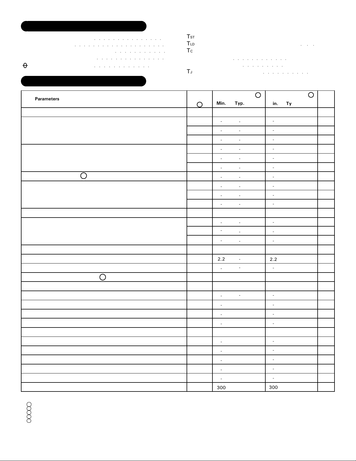
ELECTRICAL SPECIFICATIONS
Parameters
Test Conditions
All Ratings: Tc = +25°C Unless Otherwise Specified
Group A
Subgroup
5
MSK 4357H/E 3
Min.
OUTPUT CHARACTERISTICS
VC-E On Voltage (Each IGBT)
Instantaneous Forward Voltage
(FRED Flyback Diode)
Reverse Recovery Time 1
Leakage Current
IC=28A
ID=28A
ID=28A,di/dt=100A/uS,Vr=350V
V+=500V
V+=400V
V+=500V
1
2
3
1
2
3
-
1
2
3
-
-
-
-
-
-
-
-
-
-
BIAS SUPPLY CHARACTERISTICS
Quiescent Bias Current
VCC=15V
1
2
3
-
-
-
INPUT SIGNALS CHARACTERISTICS
Positive Trigger Threshold Voltage
Negative Trigger Threshold Voltage
VCC=15V
VCC=15V
1,2,3
1,2,3
2.2
-
SWITCHING CHARACTERISTICS 1
Upper Drive:
Turn-On Propagation Delay
Turn-Off Propagation Delay
Turn-On
Turn-Off
Lower Drive:
Turn-On Propagation Delay
Turn-Off Propagation Delay
Turn-On
Turn-Off
Dead Time
Minimum Pulse Width
V+=270V,VCC=15V,IC=28A
V+=270V,VCC=15V,IC=28A
4
4
4
4
4
4
4
4
-
-
-
-
-
-
-
-
-
-
-
300
NOTES:
1
Guaranteed by design but not tested. Typical parameters are representative of actual device performance but are for reference only.
2
Industrial grade and "E" suffix devices shall be tested to subgroups 1 and 4 unless otherwise specified.
3
Military grade devices ("H" suffix) shall be 100% tested to subgroups 1,2,3, and 4.
4
Subgroups 5 and 6 testing available upon request.
5
Subgroup 1,4
2,5
3,6
TA=TC=+25°C
TA=TC=+125°C
TA=TC=-55°C
Typ.
-
-
-
-
-
-
-
-
-
-
-
-
-
-
-
-
-
-
-
-
-
-
-
2
-
Max.
2.0
1.7
TBD
1.7
1.3
2.5
180
400
1.5
400
6
12
TBD
-
0.8
TBD
TBD
45
350
TBD
TBD
45
350
-
-
MSK 4357 2
Min.
-
-
-
-
-
-
-
-
-
-
-
-
-
2.2
-
-
-
-
-
-
-
-
-
-
300
Typ.
-
-
-
-
-
-
-
-
-
-
-
-
-
-
-
-
-
-
-
-
-
-
-
2
-
Max.
2.2
-
-
1.7
-
-
180
400
-
-
6
-
-
-
0.8
TBD
TBD
45
350
TBD
TBD
45
350
-
-
UNITS
V
V
V
V
V
V
nS
uA
mA
uA
mA
mA
mA
V
V
nS
nS
nS
nS
nS
nS
nS
nS
uS
uS
2
PRELIMINARY Rev. E 11/01
Page 3

APPLICATION NOTES
PROTECTIONMSK4357 PIN DESCRIPTION
VCC - is the low voltage supply for all the internal logic and
drivers. A 0.1uF ceramic capacitor in parallel with a 10uF
tantalum capacitor is recommended bypassing for the VCC-
VSS pins.
VSS - is the low voltage supply return pin and the input logic
return reference. All logic input and logic output is referenced
to this pin. This pin can vary ± 5V from the AV-,BV-,CV-/
ISENSE power return pin without affecting any of the logic
functions.
AØHIN, BØHIN, CØHIN - are low active logic inputs for signal-
ling the corresponding phase high-side switch to turn on. The
input levels are 5V CMOS or TTL compatible. Typical propa-
gation delays are around 600nS.
AØLIN, BØLIN, CØLIN - are low active inputs for signalling
the corresponding phase low-side switch to turn on. The in-
put levels are 5V CMOS or TTL compatible. Typical propaga-
tion delays are around 600nS.
ITRIP - is an analog input pin for sensing current flowing from
the AV-,BV-,CV-/ISENSE pin through a sense resistor to the
high power ground. A 0.485 volt level at this pin with re-
spect to VSS will signal an overcurrent condition and shut
down all output switching. Bringing the voltage below this
point (100 mV hysteresis) will remove the shutdown condi-
tion, and leaving the low-side logic inputs simultaneously high
(de-activated) for 10uS will restore normal operation.
All logic inputs use a 300nS filter. A pulse width below this
-
will get ignored.
VCC voltage below the cutoff level of 8.65 volts will reset all
-
switch outputs off and ignore subsequent logic inputs until
VCC is restored.
Undervoltage lockout of the internal drivers for the high-side
-
switches also occurs at 8.65 volts. This may occur if the
high-side output gets switched at greater than 25 kHZ with-
out switching the low-side. The internal power supply for the
high-side switch will sag too low for adequate switching. Ei-
ther slow down the PWM rate or PWM the low-side switches
instead.
Switching a low-side logic input while the corresponding phase
-
high-side logic input is activated will turn off both switches.
The opposite condition is also true. This is cross-conduction
lockout and will occur any time low and high-side inputs for a
phase are activated at the same time.
A 2uS deadtime is automatically inserted between high and
-
low-side output switching to allow complete turn-off of each
switch so no overlap will occur.
An overcurrent condition detected by the ITRIP pin will shut
-
down all output switches until the overcurrent condition is
removed and all three low-side logic inputs are held high for
10uS, then normal operation will resume.
AV+,BV+,CV+ - are the connections from the tops of the
three half bridges to the high voltage positive rail. Connec-
tions must be made individually from each pin to the rail, with
enough current-handling capability for the load. Proper power
supply bypassing must be connected to these three pins and
the Vss connections for proper filtering. This bypassing must
be done as close to the hybrid as possible.
AV-,BV- - are the connections from the bottoms of the AØ
and BØ half bridges to the return of the high voltage negative
rail. These pins should be tied to the CV-/ISENSE with as
short a connection as possible.
CV-/ISENSE - is the connection from the bottom of the CØ
half bridge to the return of the high voltage negative rail. There
should be a connection to AV- and BV- here. If there is cur-
rent sensing, then a sense resistor should go between this
point and the return of the high voltage supply. If no sensing
is desired, then this point should connect to Vss, the negative
rail of the high voltage supply and any high voltage bypass
capacitance.
AØ, BØ, CØ - are the pins connecting the 3 phase bridge
switch outputs.
ITRIP has a 400nS leading edge blanking time after switching
-
to ignore any switching current transients.
TYPICAL OPERATION
FIGURE 1
GROUNDING, BYPASSING, CURRENT SENSE
EXAMPLE:
FOR 20 AMP LIMIT:
R-SENSE = 0.050 OHMS
R-SENSE VOLT = 1 VOLT
R1 = 51.5 OHMS
R2 = 48.5 OHMS
3
PRELIMINARY Rev. E 11/01
Page 4

TYPICAL PERFORMANCE CURVES
4
PRELIMINARY Rev. E 11/01
Page 5
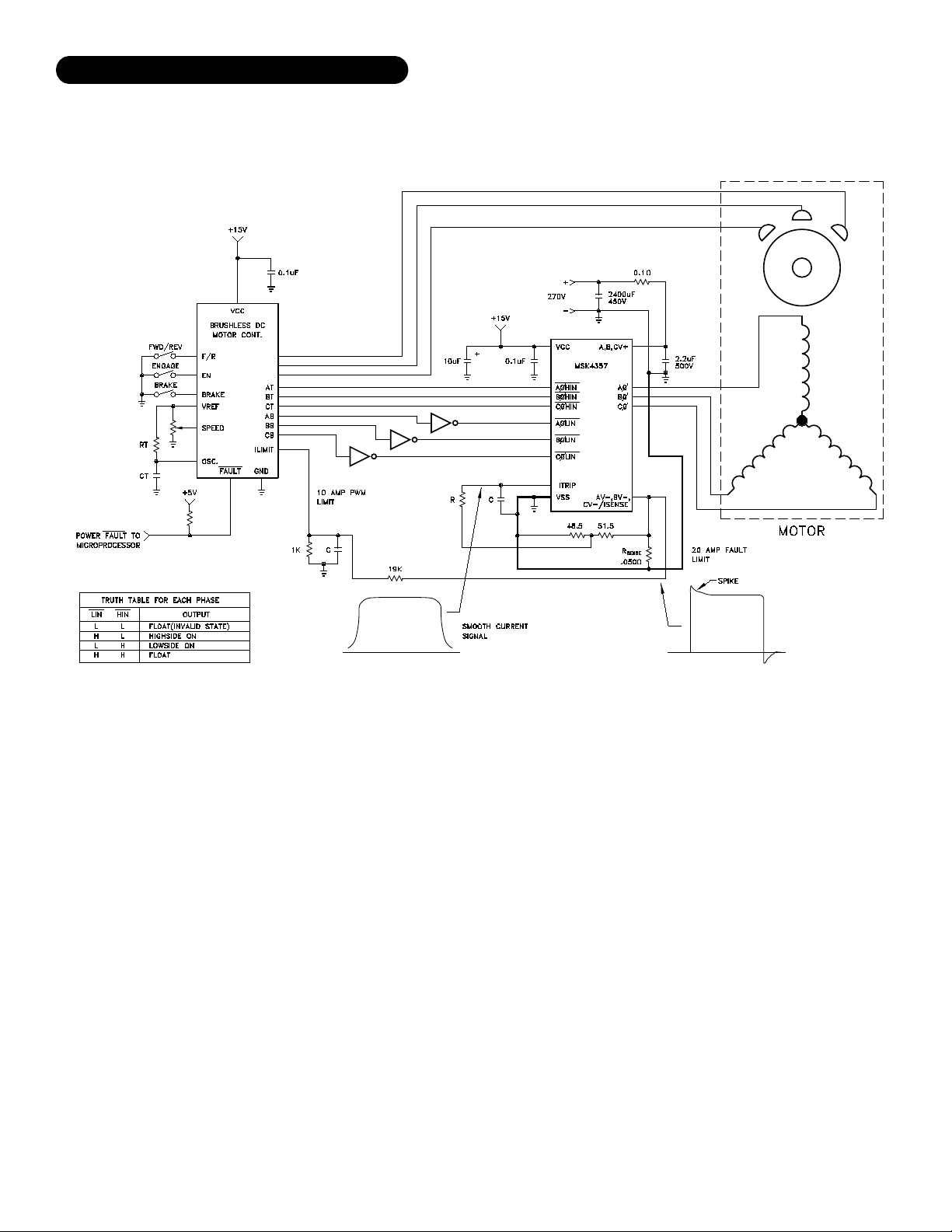
TYPICAL SYSTEM OPERATION
The MSK4357 is designed to be used with a +270 volt high voltage bus, +15 volt low power bus, and +5 volt logic signals.
Proper derating should be applied when designing the MSK4357 into a system. High frequency layout techniques with ground
planes on a printed circuit board is the only method that should be used for circuit construction. This will prevent pulse jitter caused
by excessive noise pickup on the current sense signal or the error amp signal.
Ground planes for the low power circuitry and high power circuitry should be kept separate. The connection between the bottom
of the current sense resistor, VSS pin and the high power ground are connected at this point. This is a critical path, and high
currents should not be flowing between the current sense and VSS. Inductance in this path should be kept to a minimum. An RC
filter (shown in 2 places) will filter out the current spikes and keep the detected noise for those circuits down to a minimum.
In the system shown, two types of current limit are implemented. The first limit is a PWM pulse by pulse limit controlled by the
motor controller. A second absolute maximum limit is set up for the MSK4357 which will completely shut off the bridge in the
event that current limit is exceeded.
The logic signals coming from the typical motor controller IC are set up for driving N channel low side and P channel high side
switches directly, and are usually 15 volt levels. Provision should be made for getting 5 volt logic signals to the MSK4357 of the
correct assertion levels. Typically, the low side signals out of the controller are high active and the high side are low active.
Inverters are shown in the system schematic for the low side controller output.
5
PRELIMINARY Rev. E 11/01
Page 6

MECHANICAL SPECIFICATIONS
ALL DIMENSIONS ARE ±0.010 INCHES UNLESS OTHERWISE LABELED
ORDERING INFORMATION
MSK4357 H U
LEAD CONFIGURATION
S=STRAIGHT, U=BENT UP, D=BENT DOWN
SCREENING
BLANK=INDUSTRIAL, E=EXTENDED RELIABILITY;
H=CLASS H
GENERAL PART NUMBER
THE ABOVE EXAMPLE IS A MILITARY GRADE HYBRID WITH LEADS BENT UP.
M.S. Kennedy Corp.
4707 Dey Road Liverpool, New York 13088
Phone (315) 701-6751
FAX (315) 701-6752
www.mskennedy.com
The information contained herein is believed to be accurate at the time of printing. MSK reserves the right to make
changes to its products or specifications without notice, however, and assumes no liability for the use of its products.
Please visit our website for the most recent revision of this datasheet.
PRELIMINARY Rev. E 11/016
 Loading...