

Page 1
ISO-9001 CERTIFIED BY DSCC
20 AMP, 200 VOLT MOSFET
SMART POWER 3-PHASE MOTOR
4322
M.S.KENNEDY CORP.
M.S. KENNEDY CORP.
4707 Dey Road Liverpool, N.Y. 13088 (315) 701-6751
FEATURES:
200V, 20 Amp Capability
Ultra Low Thermal Resistance - Junction to Case - 1.0°C/W (Each MOSFET)
Self-Contained, Smart Lowside/Highside Drive Circuitry
Under-Voltage Lockout, Internal 2µS Deadtime
Capable of Switching Frequencies to 25KHz
Isolated Case Allows Direct Heat Sinking
Case Bolt-down Design Allows Superior Heat Dissipation
DESCRIPTION:
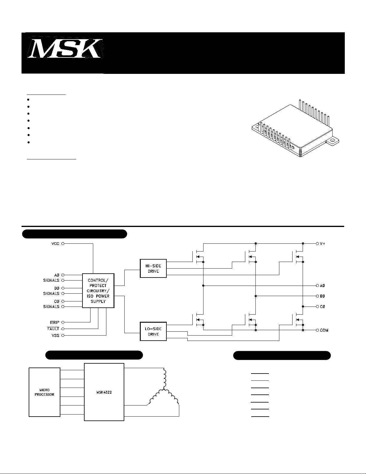
The MSK 4322 is a 20 Amp, 3 Phase Bridge Smart Power Motor Drive Hybrid with a 200 volt rating on the
output switches. The output switches are power MOSFETs with intrinsic fast-recovery diodes for the free-
wheeling currents of motor drives. This new smart power motor drive hybrid is compatible with 5V CMOS or
TTL logic levels. The internal circuitry prevents simultaneous turn-on of the in-line half bridge transistors with a
built-in 2µS deadtime to prevent shoot-through. Undervoltage lockout shuts down the bridge when the supply
voltage gets to a point of incomplete turn-on of the output switches. The internal high-side boot strap power
supply derived from the +15 volt supply completely eliminates the need for 3 floating independent power sup-
plies for the high-side drive. Current sense circuitry is provided to sense current from an external resistor to shut
down the bridge for overcurrent.
DRIVE POWER HYBRID
MIL-PRF-38534 QUALIFIED
EQUIVALENT SCHEMATIC
TYPICAL APPLICATIONS PIN-OUT INFORMATION
TYPICAL APPLICATIONSPIN-OUT INFORMATION
3 PHASE SIX STEP DC BRUSHLESS MOTOR DRIVE
OR 3 PHASE SINUSOIDAL INDUCTION MOTOR DRIVE
1
2
3
4
5
6
7
8
9
10
VCC
AØHIN
BØHIN
CØHIN
AØLIN
FAULT
CØLIN
BØLIN
VSS
ITRIP
20
19
18
17
16
15
14
13
12
11
N/C
AØ
V+
N/C
N/C
BØ
N/C
N/C
CØ
COM
1
PRELIMINARY Rev. A 6/00
Page 2
ABSOLUTE MAXIMUM RAT-
V+ High Voltage Supply. . . . . . . 200V
INGS
VCC Logic Supply . . . . . . . . . . 18V
IOUT Continuous Output Current . . . 20A
IPK Peak Output Current. . . . . . . 30A
θJC Thermal Resistance . . . . . . 1.0°C/W
(Output Switches) (Junction to Case)
ELECTRICAL SPECIFICATIONS
Storage Temperature Range
TsT
Lead Temperature Range(10 Seconds)
TLD
Case Operating Temperature
TC
MSK 4322
MSK 4322H
Junction Temperature
TJ
○○○○○○○○○○○○○○○○○
○○○○○○○○○○○○○○○○○
○○○○○○○○○○○○○○○○○
○○○○○○○○○
○○○○○○○○○
-65° to +150°C
300°C
-40°C to +85°C
-55°C to +125°C
+175°C
Parameters
OUTPUT CHARACTERISTICS
VDS(ON) (Each Transistor)
Instantaneous Forward Voltage
(Intrinsic Diode)
Reverse Recovery Time 1
Leakage Current
BIAS SUPPLY CHARACTERISTICS
Quiescent Bias Current
INPUT SIGNAL CHARACTERISTICS
Positive Trigger Threshold Voltage
Negative Trigger Threshold Voltage
SWITCHING CHARACTERISTICS
Upper Drive:
Turn-On Propagation Delay
Turn-Off Propagation Delay
Turn-On
Turn-Off
Lower Drive:
Turn-On Propagation Delay
Turn-Off Propagation Delay
Turn-On
Turn-Off
Dead Time 1
Minimum Pulse Width 1
Test Conditions
V+ = 200V
V+ = 160V
V+ = 200V
(non-switching)
V
CC = 15V
V
CC = 15V
1
V+ = 100V, V
V+ = 100V, V
ID = 20A
IS = 20A
VCC = 15V
CC = 15V, ID = 20A
CC = 15V, ID = 20A
GROUP A
SUBGROUP
5
1
2
3
1
2
3
-
1
2
3
1
2
3
1,2,3
1,2,3
-
-
-
-
-
-
-
-
-
-
MSK 4322H
Min. Typ. Max.
-
-
-
-
-
-
-
-
-
-
-
-
-
2.2
-
2.0
-
5.0
-
TBD
-
2.0
-
TBD
-
TBD
-
600
-
750
-
3.0
-
TBD
-
-
-
-
-
-
6
12
TBD
-
0.8
-
-
-
-
-
TBD
-
TBD
-
45
-
350
-
-
-
-
-
-
300
TBD
-
TBD
-
45
-
350
-
2
-
-
-
3
MSK 4322
Min. Typ. Max.
-
-
-
-
-
-
-
-
-
-
-
-
-
2.2
-
-
-
-
-
-
-
-
-
-
300
2
UNITS
2.0
-
-
-
2.0
-
-
-
600
-
750
-
-
-
-
-
-
-
0.8
-
TBD
-
TBD
-
45
-
350
-
TBD
-
TBD
-
45
-
350
-
2
-
V
-
V
-
V
V
-
V
-
V
nS
µA
-
mA
-
µA
6
mA
-
mA
-
mA
-
V
V
nS
nS
nS
nS
nS
nS
nS
nS
-
µS
-
nS
NOTES:
1 Guaranteed by design but not tested. Typical parameters are representative of actual device performance but are for reference only.
2 Industrial grade devices shall be tested to subgroups 1 and 4 unless otherwise specified.
3 Military grade devices ("H" suffix) shall be 100% tested to subgroups 1, 2, 3 and 4.
4 Subgroups 5 and 6 testing available upon request.
5 Subgroup 1, 4 TA =TC = +25°C
2, 5 TA = TC =+125°C
3, 6 TA = TC =-55°C
2
PRELIMINARY Rev. A 6/00
Page 3

TYPICAL PERFORMANCE CURVES
3
PRELIMINARY Rev. A 6/00
Page 4

APPLICATION NOTES
MSK 4322 PIN DESCRIPTION
VCC - Is the low voltage supply for all the internal logic
and drivers. A 0.1 µF ceramic capacitor in parallel with
a 10µF tantalum capacitor is recommended bypassing
for the VCC-VSS pins.
VSS - Is the low voltage supply return pin and the input
logic return reference. All logic input and logic output
is referenced to this pin. This pin can vary ±5V from
the COM power return pin without affecting any of the
logic functions.
AØHIN, BØHIN, CØHIN - Are low active logic inputs for
signalling the corresponding phase high-side switch to
turn on. The input levels are 5V CMOS or TTL compat-
ible. Typical propagation delays are around 600nS.
AØLIN, BØLIN, CØLIN - Are low active inputs for sig-
nalling the corresponding phase low-side switch to turn
on. The input levels are 5V CMOS or TTL compatible.
Typical propagation delays are around 600nS.
FAULT - Is an open drain logic output pin that gets
enabled any time the VCC level goes below the cutoff
point, or an overcurrent condition occurs. Bringing VCC
back to normal levels will reset FAULT. Removing the
overcurrent condition and allowing the low-side logic
inputs to remain high(off) for 10µS will restore opera-
tion.
PROTECTION
- All logic inputs use a 300nS filter. A pulse width
below this will get ignored.
- VCC voltage below the cutoff level of 8.65 volts
will reset all switch outputs off and ignore subse-
quent logic inputs until VCC is restored.
- Undervoltage lockout of the internal drivers for the
high-side switches also occurs at 8.65 volts, but will
not flag with the FAULT output. This may occur if
the high-side output gets switched without switch
ing the low-side. The internal boot strap power
supply for the high-side switch will sag too low for
adequate switching. The boot strap supply depends
on PWMing of the low-side switches for proper
operation.
- Switching a low-side logic input while the corre-
sponding phase high-side logic input is activated
will turn off both switches. The opposite condition
is also true. This is cross-conduction lockout and
will occur any time low and high-side inputs for a
phase are activated at the same time.
- A 2µS deadtime is automatically inserted between
high and low-side output switching to allow com-
plete turn-off of each switch so no overlap will
occur.
ITRIP - Is an analog input pin for sensing current flow-
ing from the COM pin through a sense resistor to the
high power ground. A 0.485 volt level at this pin with
respect to VSS will signal an overcurrent condition,
enable the FAULT pin and shut down all output switch-
ing. Bringing the voltage below this point (100 mV
hysteresis) will remove the FAULT output and leaving
the low-side logic inputs simultaneously high (de-acti-
vated) for 10µS will restore normal operation.
V+ - Is the high voltage positive rail for the bridge.
Proper bypassing to VSS with sufficient capacitance to
suppress any voltage transients and to ensure remov-
ing any drooping during switching, should be done as
close to the pins on the hybrid as possible.
COM - Is the return side of the bridge. A sense resistor
can be connected between this point and VSS, which
is the high voltage negative rail. COM can float above
and below the VSS pin up to 5 volts and proper opera-
tion will be maintained. Precautions should be taken
so as to not allow this voltage to get over ±5 volts
under any conditions.
AØ, BØ, CØ - Are the pins connecting the 3 phase
bridge switch outputs.
- An overcurrent condition detected by the ITRIP
pin will shut down all output switches until the
overcurrent condition is removed and all three
low-side logic inputs are held high for 10µS,
then normal operation will resume.
- ITRIP has a 100nS leading edge blanking time
after switching to ignore any switching current
transients.
TYPICAL OPERATION
4
PRELIMINARY Rev. A 6/00
Page 5

TYPICAL SYSTEM OPERATION
The MSK 4322 is designed to be used with a +100 volt high voltage bus, +15 volt low power bus and +5 volt
logic signals. Proper derating should be applied when designing the MSK 4322 into a system. High frequency
layout techniques with ground planes on a printed circuit board is the only method that should be used for circuit
construction. This will prevent pulse jitter caused by excessive noise pickup on the current sense signal or the
error amp signal.
Ground planes for the low power circuitry and high power circuitry should be kept separate. The connection
between the bottom of the current sense resistor, VSS pin and the high power ground are connected at this point.
This is a critical path and high currents should not be flowing between the current sense and VSS. Inductance in
this path should be kept to a minimum. An RC filter (shown in 2 places) will filter out the current spikes and keep
the detected noise for those circuits down to a minimum.
In the system shown, two types of current limit are implemented. The first limit is a PWM pulse by pulse limit
controlled by the motor controller. A second absolute maximum limit is set up for the MSK 4322 which will
completely shut off the bridge in the event that current limit is exceeded.
When controlling the motor speed by the PWM method, it is required that the low side switches be PWM pulsed
due to the charge pump power supplies used to power the high side switch drives. The higher the PWM speed the
higher the current load on the drive supply. PWM of the low side will prevent sagging of the high side supplies.
The logic signals coming from the typical motor controller IC are set up for driving N channel low side and P
channel high side switches directly and are usually 15 volt levels. Provision should be made for getting 5 volt logic
signals to the MSK 4322 of the correct assertion levels. Typically, the low side signals out of the controller are
high active and the high side are low active. Inverters are shown in the system schematic for the low side control-
ler output.
5
PRELIMINARY Rev. A 6/00
Page 6

MECHANICAL SPECIFICATIONS
ESD Triangle Indicates Pin 1
All dimensions are ±0.01 inches unless otherwise specified.
MSK4322 H U
4707 Dey Road, Liverpool, New York 13088
ORDERING INFORMATION
LEAD CONFIGURATIONS
S = STRAIGHT; U = BENT UP; D = BENT DOWN
SCREENING
BLANK = INDUSTRIAL; H = MIL-PRF-38534
GENERAL PART NUMBER
M.S. Kennedy Corp.
Phone (315) 701-6751
FAX (315) 701-6752
www.mskennedy.com
The information contained herein is believed to be accurate at the time of printing. MSK reserves the right to make
changes to its products or specifications without notice, however and assumes no liability for the use of its products.
6
PRELIMINARY Rev. A 6/00
 Loading...