

Page 1
ISO 9001 CERTIFIED BY DSCC
29 AMP, 75V, 3 PHASE MOSFET
BRIDGE WITH INTELLIGENT
4301
M.S.KENNEDY CORP.
4707 Dey Road Liverpool, N.Y. 13088 (315) 701-6751
INTEGRATED GATE DRIVE
FEATURES:
75 Volt Motor Supply Voltage
29 Amp Output Switch Capability, All N-Channel MOSFET Output Bridge
100% Duty Cycle High Side Conduction Capable
Suitable for PWM Applications from DC to 100KHz
Shoot-Through/Cross Conduction Protection
Undervoltage Lockout Protection
Programmable Dead-Time Control
Low Active Enable for Bridge Shutdown Control
Isolated Package Design for High Voltage Isolation Plus Good Thermal Transfer
Available with Three Lead Bend Options
MIL-PRF-38534 QUALIFIED
DESCRIPTION:
The MSK 4301 is a 3 phase MOSFET bridge plus drivers in a convenient isolated hermetic package. The hybrid is
capable of 29 amps of output current and 75 volts of DC bus voltage. It has a full line of protection features, including
undervoltage lockout protection of the bias voltage, cross conduction control and a user programmable dead-time control for
shoot-through elimination. In addition, the bridge may be shut down by using the Enable control. The MSK 4301 provides
good thermal conductivity for the MOSFETs due to the electrically isolated package design that allows direct heat sinking
of the device without insulators.
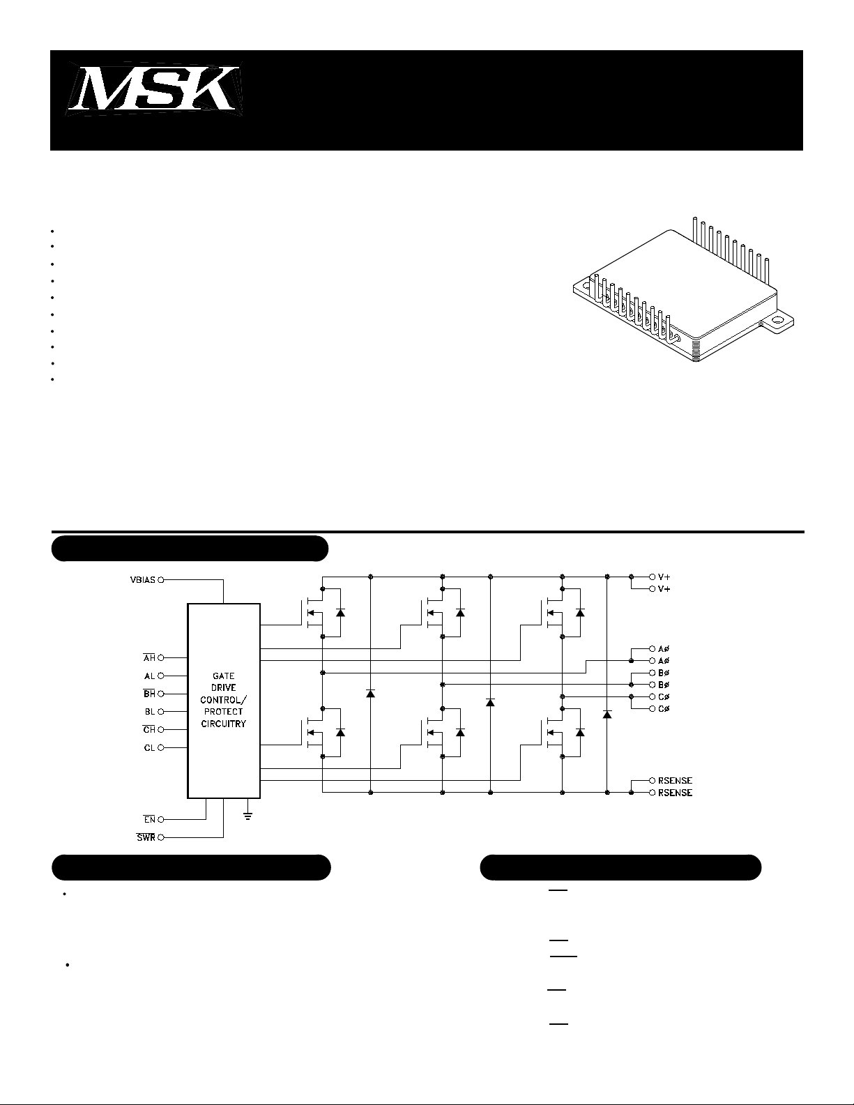
EQUIVALENT SCHEMATIC
TYPICAL APPLICATIONS
3 Phase Brushless DC
Servo Control
Fin Actuator Control
Gimbal Control
3 Phase AC
Induction Motor Control
HVAC Blower Control
PIN-OUT INFORMATION
BH
1
BL
2
AL
3
AH
4
SWR
5
VBIAS
6
EN
7
CL
8
CH
9
GND
10
1
20
19
18
17
16
15
14
13
12
11
AØ
AØ
V+
V+
BØ
BØ
CØ
CØ
RSENSE
RSENSE
Rev. D 4/01
Page 2

ABSOLUTE MAXIMUM RATINGS
V+
High Voltage Supply
VBIAS
Bias Supply
VIND
Logic Input Voltages
IOUT
Continuous Output Current
IPK
Peak Output Current
○○○○○○○○○○○○○○○○○○○○
○○○○○○○○○○○○○○○
○○○○
-0.3V to VBIAS +0.3V
○○○○○○○○○○○
○○○○○○○○○○○○○○○
ELECTRICAL SPECIFICATIONS
75V
16V
29A
41A
θJC
Thermal Resistance
TST
Storage Temperature Range
TLD
Lead Temperature Range
(10 Seconds)
TC
Case Operating Temperature
(4301H/E)
(4301)
TJ
Junction Temperature
○○○○○○○○○○○○○○○
○○○○○○○○○○○○○○○○
MMS
○○○○○○○○○○○○○○
-65°C to +150°C
○○○
○○○○○○○○○○
+300°C
-55°C to +125°C
-40°C to +85°C
○○○○○○○○○○○○
+150°C
1°C/W
Parameter
CONTROL SECTION
VBIAS Quiescent Current
VBIAS Operating Current
Undervoltage Threshold (Falling)
Undervoltage Threshold (Rising)
Low Level Input Voltage
High Level Input Voltage
Low Level Input Current
High Level Input Current
OUTPUT BRIDGE
Drain-Source Breakdown Voltage
Drain-Source Leakage Current
Drain-Source On Resistance (Each FET)
Drain-Source On Resistance
(Each FET, For Thermal Calculations Only)
SWITCHING CHARACTERISTICS
Rise Time
Fall Time
Turn-On Prop Delay (Lower)
Turn-Off Prop Delay (Lower)
Turn-On Prop Delay (Upper)
Turn-Off Prop Delay (Upper)
Dead Time
Dead Time
SOURCE-DRAIN DIODE CHARACTERISTICS
Forward Voltage
Reverse Recovery Time
1
1
1
1
1
1
1
1
1
f=20KHz, 50% Duty Cycle
1
1
Test Conditions
All Inputs Off
VIN=0V
VIN=5V
ID=25µA, All Inputs Off
VDS=70V
ID=29A
V+=28V, RL=1Ω
ID=29A
SWR Resistor=∞
SWR Resistor=∞
SWR Resistor=∞
SWR Resistor=∞
SWR =∞
SWR=12K
ISD=29A
ISD=29A, di/dt=100A/µS
GroupA 4
Subgroup
1,2,3
1,2,3
1
1
-
-
-
-
-
-
1
-
-
-
4
4
4
4
4
4
-
-
MSK4301H/E
60
-1
70
Typ.
2.5
-
-
-
-
-
-
-
-
-
-
-
-
-
-
20
6.6
7.1
100
120
81
0.5
0.5
5.0
1.0
1.05
120
Min.
5.75
6.2
2.7
3.0
0.3
3 2
Max.
8
25
7.5
8.0
0.8
-
-
-
-
-
-
5
5
-
135
+1
-
25
0.020
0.013
-
-
2
8
8
2
7.0
1.2
1.30
-
MSK4301
Min.
-
-
5.75
6.2
-
2.7
60
-1
70
-
-
--
-
-
-
-
-
-
3.0
0.3
-
-
Typ.
2.5
20
6.6
7.1
-
-
100
-
-
-
-
-
120
81
0.5
5
5
0.5
5.0
1.0
1.05
120
Max.
8
25
7.5
8.0
0.8
-
135
+1
-
25
0.020
0.013
-
-
3
10
10
3
7.0
1.2
1.30
-
Units
mAmp
mAmp
Volts
Volts
Volts
Volts
µAmp
µAmp
V
µAmp
Ω
Ω
nSec
nSec
µSec
µSec
µSec
µSec
µSec
µSec
Volts
nSec
NOTES:
1 Guaranteed by design but not tested. Typical parameters are representative of actual device
performance but are for reference only.
2 Industrial grade and "E" suffix devices shall be tested to subgroups 1 and 4 unless otherwise specified.
3 Military grade devices ("H" Suffix) shall be 100% tested to Subgroups 1, 2, 3 and 4.
4 Subgroups 5 and 6 testing available upon request.
5 Subgroup 1, 4 T
2, 5 T
3, 6 T
A = TC = +25°C
A = TC = +125°C
A = TC = -55°C
2
Rev. D 4/01
Page 3

APPLICATION NOTES
MSK 4301 PIN DESCRIPTIONS
AL,BL,CL - Are the lowside logic level digital inputs. These
three inputs control the three lowside bridge transistors. If the
highside inputs are low, then the lowside inputs will control
both the lowside and the highside of the bridge, with deadtime
set by the SWR resistor. EN will override these inputs, forcing
all outputs low. These inputs can be driven by logic up to 15V
(less than VBIAS). An internal pullup to VBIAS will hold each
input high if the pins are not driven.
AH,BH,CH - Are the highside logic level digital inputs. These
three inputs control the three highside bridge transistors. Un-
less the deadtime is disabled by connecting SWR to ground,
the lowside input of each phase will override the corresponding
highside input. If SWR is the lowside input of each phase will
override the corresponding highside input. In this condition,
tied to ground, deadtime is disabled and the outputs follow the
inputs. In this condition, shoot-through must be avoided exter-
nally. EN will override all inputs, forcing outputs low.
VBIAS - Is the positive supply for the gate drive. This pin should
be decoupled to ground with at least a 22µF capacitor in parallel
with a 0.1µF ceramic capcitor.
BUS VOLTAGE FILTER CAPACITORS
The size and placement of the capacitors for the main voltage
bus for the motor will have an effect on the noise filtered through-
out the rest of the system. Series RLC tuned circuit is being
created by the inductance of the wire (about 30nH per inch),
the filter capacitance, and all of the resistances (wire resistance
and the capacitor ESR) of the overall power circuit. Voltage
spikes from the back EMF if the motor ride on top of the bus
voltage. All of this must be taken into account when laying out
the system. A first capacitor of high quality and low ESR should
be placed as close to the hybrid circuit as possible. Along with
that, a capacitor of 5x to 10x the first value should be added
(and that second capacitor should have some ESR) and/or a
resistor should be added to help with the damping of the volt-
age spikes. Be careful of the ripple current in all the capacitors.
Excessive ripple current, beyond what the capacitor is rated
for, will destroy the capacitor.
GROUND - Is the return for the VBIAS supply. This pin should
be connected to the return of the lowside MOSFETs or the
bottom of the sense resistor at the bottom of the bridge. The
gate drive current must return through this pin, so trace lengths
should be kept to a minimum. All grounds should be returned
to the bottom of the bridge or sense resistor in a star fashion.
This will eliminate ground loops.
SWR - Is the pin for controlling the deadtime between the top
and bottom transistors of the bridge. By connecting a pullup
resistor between this pin and VBIAS, various deadtimes can be
obtained. There is and internal 100KΩ pullup resistor connected
internally. By adding additional resistors in externally, reduced
deadtimes can be achieved. By connecting this pin directly to
ground, all deadtime is eliminated. However, care must be taken
to assure that deadtime is being generated by the logic circuitry
driving the inputs. Shoot-through can occur (both the top and
bottom transistors on at the same time for a given phase, caus-
ing a short on the V+ supply to ground) destroying the bridge.
V+ - Is the power connection for the top of the output bridge.
These pins must be bypassed by a capacitor to ground of a least
10µF per amp preferrably 100µF per amp of output current mini
mum, high quality high frequency bypass capacitance to help
suppress switching noise. Connect both pins for proper current
sharing.
A
Ø, BØ, CØ - Are the output pins for the three phases of power
bridge. Connect both pins for proper current sharing.
BIAS SUPPLY BYPASS CAPACITORS
It is recommended that at least 22µF of capacitance for bypass-
ing the VBIAS voltage that supplies the drive circuitry for the
MSK 4301, along with 0.1µF for helping the high frequency
current pulses needed by the gate driver. If an extremely long
risetime is exhibited by the turn on of the FETs, the extra high
frequency capacitance will help.
GENERAL LAYOUT
Good high frequency PC layout techniques are a must. Traces
wide enough for the current delivered, and placement of the big
capacitors close to the MSK 4301 are very important. The path
for the RSENSE connection through any sense resistor back to
the GND pins must be as short as possible. This path is the
gate drive current path for all the FETs on the lower half of each
phase. A short, low inductance path will aid in the switching
time of those FETs.
IN
EN - Is the enabling input for the bridge. This digital input,
when pulled low, will enable the bridge, following the inputs
from AL, BL, CL and AH, BH, CH inputs. When pulled high, it
will override all other inputs and disable the bridge. It is inter-
nally pulled high to VBIAS, and can be driven by logic levels up
to VBIAS.
RSENSE - Are the connections to the bottom of the bridge. All
power flowing through the bridge will flow through this point,
and can be sensed by connecting a sense resistor from here to
ground. The sense resistor will develop a voltage proportional
to the current flowing. Size the value and power rating of the
sense resistor according to the voltage necessary. 3 volts is
the maximum voltage between this point and ground, or dam-
age to the hybrid will result. Connect both pins for proper cur-
rent sharing.
LOW POWER STARTUP
When starting up the circuit utilizing the MSK 4301 for the first
time, it is very important to keep certain things in mind. Be-
cause of the small size of the bridge, there is no internal short
circuit protection and a short circuit will destroy the bridge.
Any required short circuit protection must be built outside the
bridge. Current and voltage limit the power supply feeding the
V+ pins to the bridge, and monitor the current for any signs of
short circuiting, or shoot-through currents. If there are large
current spikes at the beginning of each switching cycle, there
may be shoot through. Try raising the resistor value of the
SWR. This will lengthen the deadtime and stop shoot-through.
3
Rev. D 4/01
Page 4

TYPICAL APPLICATION SCHEMATIC
TYPICAL PERFORMANCE CURVES
4
Rev. D 4/01
Page 5

MECHANICAL SPECIFICATIONS
ESD Triangle Indicates Pin 1.
NOTE: ALL DIMENSIONS ARE ±.010 INCHES UNLESS OTHERWISE LABELED.
MSK4301 H U
The above example is a Military grade hybrid with leads bent up.
ORDERING INFORMATION
LEAD CONFIGURATIONS
S= STRAIGHT; U= BENT UP; D= BENT DOWN
SCREENING
BLANK= INDUSTRIAL; E = EXTENDED RELIABILITY;
H = CLASS H
GENERAL PART NUMBER
M.S. Kennedy Corp.
4707 Dey Road, Liverpool, New York 13088
Phone (315) 701-6751
FAX (315) 701-6752
www.mskennedy.com
The information contained herein is believed to be accurate at the time of printing. MSK reserves the right to make
changes to its products or specifications without notice, however, and assumes no liability for the use of its products.
Please visit our website for the most recent revision of this datasheet.
5
Rev. D 4/01
 Loading...