

Page 1

ISO 9001 CERTIFIED BY DSCC
DUAL HIGH POWER
M.S. KENNEDY CORP
4707 Dey Road Liverpool, N.Y. 13088 (315) 701-6751
FEATURES:
Available as SMD #5962-9083801 HX
High Output Current - 10 Amps Peak
Wide Power Supply Range - ±10V to ±40V
On Board Current Limit
FET Input
Isolated Case
Second Source for OMA 2541SKB
DESCRIPTION:
The MSK 2541 is a high power dual monolithic amplifier ideally suited for high power amplification and magnetic
deflection applications. This amplifier is capable of operation at a supply voltage rating of 80 volts and can deliver
guaranteed continuous output currents up to 5A per amplifier. The MSK 2541 has internal current limit circuitry to
protect the amplifier and load from transients. The MSK 2541 is available in a hermetically sealed 8 pin TO3 package
that is isolated from internal circuitry. This allows for convenient bolt down heat sinking when necessary.
EQUIVALENT SCHEMATIC
OP-AMP
MIL-PRF-38534 CERTIFIED
2541
TYPICAL APPLICATIONS
Servo Amplifer
Motor Driver
Audio Amplifier
Programmable Power Supply
Bridge Amplifier
PIN-OUT INFORMATION
1 Output B 8 Inverting Input B
2 Positive Power Supply 7 Non-Inverting Input B
3 Non-Inverting Input A 6 Negative Power Supply
4 Inverting Input A 5 Output A
1
Rev. B 8/00
Page 2
ABSOLUTE MAXIMUM RATINGS
±V
CC Voltage Supply ±40V
OUT Peak Output Current See S.O.A.
I
IN Differential Input Voltage ±VCC
V
VIN Common Mode Input Voltage ±VCC
TC Case Operating Temperature Range
MSK 2541B -55° to +125°C
MSK 2541 -40° to +85°C
○○○○○○○○○○○○
○○○○○○○
○○○○○○○
○○○○○
○○○○○○○○○○○○
○○○○○○○○○○○○
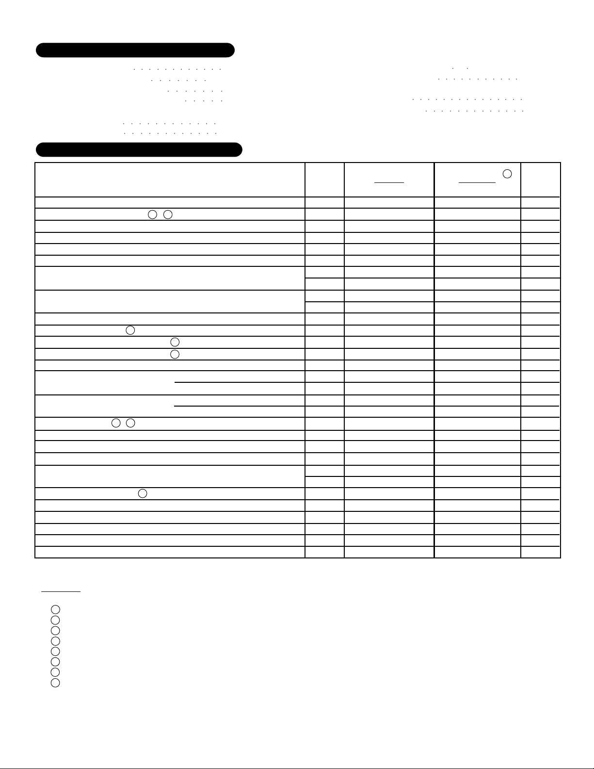
ELECTRICAL SPECIFICATIONS
Parameter
STATIC
Supply Voltage Range
Quiescent Current
2
Total - Both Amplifiers V
INPUT
Input Offset Voltage
Input Offset Voltage Drift
Input Bias Current
Input Bias Current
Input Capacitance
Input Impedance
Common Mode Rejection Ratio
Power Supply Rejection Ratio
4
F = DC V
V
OUTPUT
Output Voltage Swing
Output Current
4
Settling Time
3
Power Bandwidth
TRANSFER CHARACTERISTICS
Slew Rate
Open Loop Voltage Gain
THERMAL RESISTANCE
4
θJC (Junction to Case)
θJC
One Amplifier, AC Output F > 60 Hz
θJC
θJC
Both Amplifiers, AC Output F > 60 Hz
θJA (Junction to Ambient)
Test Conditions
4
IN = 0V
V
V
IN = 0V
V
CM = 0V
Either Input
VCM = 0V
F = DC
4
CC = ±10V to ±40V
4
L = 5.6Ω F ≤ 10 KHz
R
R
L = 10Ω F = 10 KHz
R
L = 5.6Ω F ≤ 10 KHz
R
L = 10Ω F = 10 KHz
0.1% 2V step
R
L = 10Ω VO = 20 VRMS
VOUT = ±10V RL = 10Ω
F = 10 Hz R
One Amplifier, DC Output
Both Amplifiers, DC Output
No Heat Sink
IN = 0V
CM = ±22V
L = 10 KΩ
TST Storage Temperature Range -65° to +150°C
TLD Lead Temperature Range 300°C
○○
○○○○○○○○○○○
(10 Seconds)
PD Power Dissipation 125W
TJ Junction Temperature 150°C
MSK 2541B
Group A
Subgroup
-
1, 2, 3
1
2, 3
1
2, 3
1
2, 3
-
-
-
-
4
5, 6
4
5, 6
-
4
4
4
5, 6
-
-
-
-
-
Military Industrial
Min.
±10
Typ.
±35
±40
-
±0.1
-
±15
-
±4
-
±10
-
2.0
-
-
-
10
-
95
±28
±30
±5
113
-
90
±29
±31
±8
±3.0
-
45
6
95
55
10
100
85
-
1.4
-
1.25
-
0.9
-
0.8
-
30
○○○○○○○○○○○○○○○
○○○○○○○○○○○○○
MSK 2541
Max.
±40
±60
±1.0
±30
±50
±50
30
20
-
5
-
12
-
-
-
-
-
-
-
2
-
-
-
-
-
-
-
1.9
1.5
1.2
1.0
-
Min.
±10
-
-
-
-
-
-
-
-
-
90
-
±28
-
±5
-
-
40
6
90
-
-
-
-
-
-
Typ.
±35
±40
±1.0
±15
±10
±29
1.25
±4
2.0
5
10
113
90
±8
2
50
10
100
1.4
0.9
0.8
30
5
Max.
±40
±60
±10
±100
-
12
-
-
-
30
1.9
1.5
1.2
1.0
Units
V
mA
mV
-
µV/°C
pA
-
nA
pA
-
nA
-
-
-
-
-
-
-
-
-
-
-
-
-
pF
W
dB
dB
V
V
A
A
µS
KHz
V/µS
dB
dB
°C/W
°C/W
°C/W
°C/W
-
°C/W
NOTES:
1 Unless otherwise specified: RCL = 0Ω, ±VCC = ±34 VDC, all specs are per amplifier.
2 Electrical specifications are derated for power supply voltages other than ±34 VDC.
3 AV = -1, measured in false summing junction circuit.
4 Devices shall be capable of meeting the parameter, but need not be tested. Typical parameters are for reference only.
5 Industrial grade devices shall be tested to subgroups 1 and 4 unless otherwise specified.
6 Military grade devices ('B' suffix) shall be 100% tested to subgroups 1, 2, 3 and 4.
7 Subgroup 5 and 6 testing available upon request.
8 Subgroup 1, 4 TA=TC=+25°C
Subgroup 2, 5 TA=TC=+125°C
Subgroup 3, 6 TA=TC=-55°C
2
Rev. B 8/00
Page 3

APPLICATION NOTES
HEAT SINKING
To select the correct heat sink for your application, refer to the
thermal model and governing equation below.
Thermal Model:
Governing Equation:
TJ = PD X (RθJC + RθCS + RθSA) + TA
Where
TJ = Junction Temperature
PD = Total Power Dissipation
RθJC = Junction to Case Thermal Resistance
RθCS = Case to Heat Sink Thermal Resistance
RθSA = Heat Sink to Ambient Thermal Resistance
C = Case Temperature
T
TA = Ambient Temperature
TS = Sink Temperature
POWER SUPPLY CONNECTIONS
The MSK 2541 maximum supply voltage is specified as
±40V. However, single sided or unbalanced power supply
operation is permissible as long as the total power supply volt-
age does not exceed 80V. Caution should be exercised when
routing high current printed circuit paths. Generally, these
paths should not be placed near low level, high impedance
input circuitry to avoid oscillations.
During prototype evaluation, power supply current limiting
is strongly advised to avoid damaging the device. See the
application note entitled "Current Limit" for an explanation of
the limitations of the MSK 2541 on board current limit.
POWER SUPPLY BYPASSING
Both the negative and the positive power supplies must be
effectively decoupled with a high and low frequency bypass
circuit to avoid power supply induced oscillation. An effective
decoupling scheme consists of a 0.1 microfarad ceramic ca-
pacitor in parallel with a 4.7 microfarad tantalum capacitor
from each power supply pin to ground. It is also a good prac-
tice with very high power op-amps, such as the MSK 2541, to
place a 30-50 microfarad non-electrolytic capacitor with a low
effective series resistance in parallel with the other two power
supply decoupling capacitors. This capacitor will eliminate
any peak output voltage clipping which may occur due to poor
power supply load regulation. All power supply decoupling
capacitors should be placed as close to the package power
supply pins as possible (pins 3 and 6).
CURRENT LIMIT
Example:
In our example the amplifier application requires each output to
drive a 20 volt peak sine wave across a 10 ohm load for 2 amps of
output current. For a worst case analysis we will treat the 2 amps
peak output current as a D.C. output current. The power supplies
are ±35 VDC.
1.) Find Power Dissipation
PD = [(quiescent current) X (+VCC - (-VCC))] + [(VCC - VO) X IOUT]
= (30 mA) X (70V) + (15V) X (2A)+(15V)x(2A)
= 2.1W + 60W
= 62.1W
2.) For conservative design, set TJ = +150°C
3.) For this example, worst case TA = +25°C
4.) RθJC = 1.2°C/W typically
5.) RθCS = 0.15°C/W for most thermal greases
6.) Rearrange governing equation to solve for RθSA
RθSA =(TJ - TA) / PD - (RθJC) - (RθCS)
= (150°C - 25°C) / (62.1W) - (1.2°C/W) - (.15°C/W)
= ≅.66°C/W
The heat sink in this example must have a thermal resistance of
no more than .66°C/W to maintain a junction temperature of no
more than +150°C. Since this value of thermal resistance may be
difficult to find, other measures may have to be taken to decrease
the overall power dissipation. Refer to the "Heat Sinking Options"
application note offered by MSK.
The internal current limit should not be used as a short cir-
cuit protection scheme. When the output is directly shorted
to ground, the power supply voltage is applied across the out-
put transistor that is conducting. If the power supplies were
set to ±40V and the output was shorted to ground, the tran-
sistor that is conducting current would see 40V from its emit-
ter to its collector. Referring to the safe operating area curve
shows when [VCC-VOUT]=40V, the maximum safe output
current (IO) at TC=25°C is 1.5A. In this case the amplifier
would not be protected by the internal current limit and would
probably be damaged. The internal current limit is provided as
a protection against unintentional load conditions which may
require larger amounts of load current than the amplifier is
rated for.
SAFE OPERATING AREA
The safe operating area curve is a graphical representation
of the power handling capability of the amplifier under various
conditions. The wire bond current carrying capability, transis-
tor junction temperature and secondary breakdown limitations
are all incorporated into the safe operating area curves. All
applications should be checked against the S.O.A. curves to
ensure high M.T.T.F.
3
Rev. B 8/00
Page 4

TYPICAL PERFORMANCE CURVES
4
Rev. B 8/00
Page 5

APPLICATION CIRCUITS
CLAMPING OUTPUT FOR EMF-GENERATING LOADS
ISOLATING CAPACITVE LOADS
PROGRAMMABLE VOLTAGE SOURCE
PARALLELED OPERATION, EXTENDED S.O.A.
5
Rev. B 8/00
Page 6

MECHANICAL SPECIFICATIONS
ALL DIMENSIONS ARE ±0.010 INCHES UNLESS OTHERWISE SPECIFIED.
ORDERING INFORMATION
Part
Number
MSK2541
MSK2541B
5962-9083801HX
Screening Level
Industrial
Military-MIL-PRF-38534
DSCC - SMD
M.S. Kennedy Corp.
4707 Dey Road, Liverpool, New York 13088
Phone (315) 701-6751
Fax (315) 701-6752
www.mskennedy.com
The information contained herein is believed to be accurate at the time of printing. MSK reserves the right to make
changes to its products or specifications without notice, however and assumes no liability for the use of its products.
6
Rev. B 8/00
 Loading...