

Page 1
ISO 9001 CERTIFIED BY DSCC
HIGH SPEED/VOLTAGE
OP AMP
1461
M.S.KENNEDY CORP.
4707 Dey Road Liverpool, N.Y. 13088 (315) 701-6751
FEATURES:
Extremely Fast - 500v/µS
Wide Supply Range ±15V to ±45V
VMOS Output, No S.O.A. Restrictions
Large Gain-Bandwidth Product
FET Input
Electrically Isolated Case
800mA Typical Output Current
MIL-PRF-38534 CERTIFIED
DESCRIPTION:
The MSK 1461 is a state of the art high speed FET input operational amplifier. The distinguishing characteristic
of the MSK 1461 is its unique VMOS output stage which completely eliminates the safe operating area restrictions
associated with secondary breakdown of bipolar transistor output stage op-amps. Freedom from secondary break-
down allows the 1461 to handle large output currents at any voltage level limited only by transistor junction tempera-
ture. 115 dB of open loop gain gives the 1461 high closed loop gain accuracy and the typical ±1.0mV of input offset
voltage will fit well in any error budget. A 500 V/µS slew rate and 1200 MHz gain bandwidth product make the 1461
an outstanding high-speed op-amp. A single external capacitor is used for compensation and output current limiting
is user programmable through the selection of two external resistors.
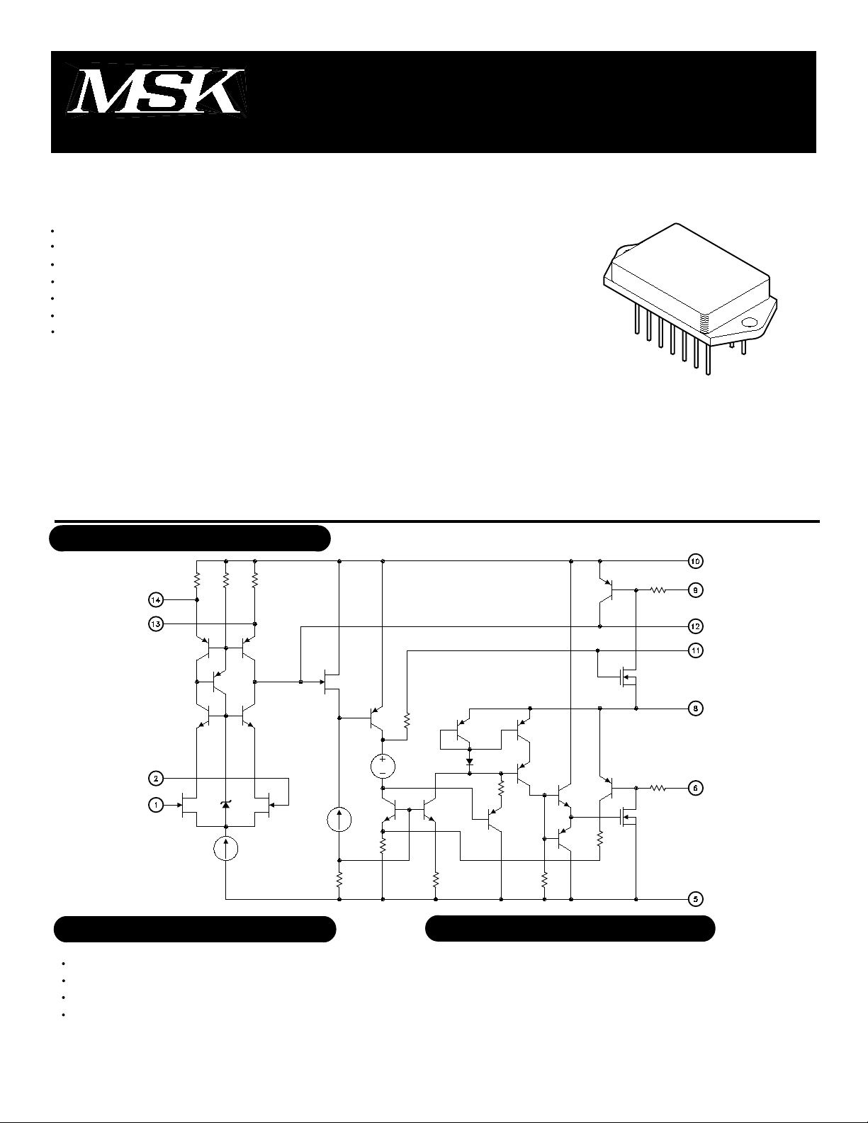
EQUIVALENT SCHEMATIC
TYPICAL APPLICATIONS
PIN-OUT INFORMATION
Video Yoke Drivers
Video Distribution Amplifiers
High Accuracy Audio Amplification
High Speed ATE Pin Drivers
Inverting Input
1
Non-Inverting Input
2
No Connection
3
No Connection
4
Negative Power Supply
5
Negative Current Limit
6
No Connection
7
1
8
Output
9
Positive Current Limit
10
Positive Power Supply
11
Compensation
12
Compensation
13
Offset Adjust
14
Offset Adjust
Rev. B 8/00
Page 2
ABSOLUTE MAXIMUM RATINGS
±VCC
Supply Voltage
IOUT
Output Current
VIN
Differential Input Voltage
RTH
Thermal Resistance
○○○○○○○○○○○○○○○○
○○○○○○○○○○○○○○○
○○○○○○○○○○○○
Junction to Case
(Output Devices Only)
ELECTRICAL SPECIFICATIONS
Parameter
STATIC
Supply Voltage Range
Quiescent Current
Thermal Resistance
INPUT
Input Offset Voltage
Input Offset Voltage Drift
Input Offset Adjust
Input Bias Current
Input Offset Current
Input Impedance
Common Mode Range
Common Mode Rejection Ratio
OUTPUT
Output Voltage Swing
Output Current, Peak
Settling Time
2
TRANSFER CHARACTERISTICS
Slew Rate
Open Loop Voltage Gain
Gain Bandwidth Product
3
3
3
3
3
3
3
3
VOUT=±10V RL=1KΩ AV=-5V/V
3
3
±45V
800mA
○○○○○○○○○○
±25V
12°C/W
Test Conditions
VIN=0V
Junction to Case
VIN=0V AV=-10V/V
Bal. Pins=N/C
RPOT=10KΩ to +VCC
VCM=0V
Either Input
VCM=0V
F=DC
F=10KHz VCM=±22V
RL=50Ω AV=-5V/V
RL=1KΩ
RL=33Ω AV=-5V/V TJ<175°C
0.1% 10V step
RL=1KΩ F=100Hz
F=100KHz
Storage Temperature Range
TST
Lead Temperature Range
TLD
(10 Seconds)
Case Operating Temperature
TC
(MSK 1461B)
(MSK 1461)
Junction Temperature
TJ
Group A
Subgroup
-
1
2,3
-
1
2,3
-
1
2,3
-
-
-
-
4
4
4
4
4
4
4
4
Min.
±15
±22
±27
±30
±600
200
800
○○○○○○○○○○
○○○○○○○○○○○○○
Typ.
-
±19
-
±21
-
11
-
±1.0
-
±6.0
-
±8.0
-
±10
-
±10
-
±5.0
-
±5.0
-
3x10
-
±24
100
90
±31
±33
±800
400
-
500
106
90
1200
-65°C to +150°C
○○○○○○○○○○
-55°C to +125°C
○○○○○○○○○○○
MSK 1461MSK 1461B
Typ.
12
Min.
±15
±19
-
-
-
±1.0
-
±10
-
±8.0
-
-
±10
-
-
±5.0
-
-
-
-
-
-
-
-
-
-
-
-
-
-
±22
90
±27
±30
±600
-
200
90
800
3x10
±24
100
±31
±33
±800
400
500
106
1200
Max.
±45
±25
±35
±5.0
±50
±300
±100
800
300°C
-40°C to 85°C
+175°C
Max.
-
±45
±28
-
-
11
15
±8.0
-
µV/°C
-
±300
-
-
-
-
-
1212
-
-
-
-
-
-
800
-
-
-
Units
V
mA
mA
°C/W
mV
V
pA
nA
pA
nA
Ω
V
dB
V
V
mA
nS
V/µS
dB
MHz
NOTES:
1
RSC=0Ω and ±VCC=36VDC unless otherwise specified.
2
AV=-1, measured in false summing junction circuit.
3
Devices shall be capable of meeting the parameter, but need not be tested. Typical parameters are for reference only.
4
Industrial grade devices shall be tested to subgroups 1 and 4 unless otherwise specified.
5
Military grade devices ("B" suffix) shall be 100% tested to subgroups 1,2,3 and 4.
6
Subgroups 5 and 6 testing available upon request.
7
Subgroup 1,4
Subgroup 2,5
Subgroup 3,6
TC=+25°C
TJ=+125°C
TA=-55°C
Rev. B 8/002
Page 3

APPLICATION NOTES
HEAT SINKING
To select the correct heat sink for your application,
refer to the thermal model and governing equation below.
Thermal Model:
Governing Equation:
TJ=PD x (RθJC + RθCS + RθSA) + TA
Where
TJ = Junction Temperature
PD = Total Power Dissipation
RθJC = Junction to Case Thermal Resistance
RθCS = Case to Heat Sink Thermal Resistance
RθSA = Heat Sink to Ambient Thermal Resistance
TC = Case Temperature
TA = Ambient Temperature
TS = Sink Temperature
CURRENT LIMIT
The output current of the MSK 1461 is internally lim-
ited to approximately ±750mA by two 0.8Ω internal cur-
rent limit resistors. Additional current limit can be achieved
through the use of two external current limit resistors.
One resistor (+RSC) limits the positive output current and
the other (-RSC) limits the negative output current. The
value of the current limit resistors can be determined as
follows:
±RSC = [(0.65V/±ILIM) - 0.8Ω]
Since the 0.65V term is obtained from the base to
emitter voltage drop of a bipolar transistor, the equation
only holds true for +25°C operation. As case tempera-
ture increases, the 0.65V term will decrease making the
actual current limit set point decrease slightly.
The following schematic illustrates how to connect
each current limit resistor:
INPUT OFFSET ADJUST CONNECTION
IN
Example:
In our example the amplifier application requires the
output to drive a 20 volt peak sine wave across a 400Ω
load for 50mA of peak output current. For a worst case
analysis we will treat the 50mA peak output current as a
D.C. output current. The power supplies shall be set to
±40VDC.
1.) Find Driver Power Dissipation
PD = [(quiescent current) x (+VS - (-VS))] +
[(+VS-VO) x IOUT]
= [(50mA) x (80V)] + [(20V) x (0.05A)]
= 4W + 1.0W
= 5Watts
2.) For conservative design, set TJ=+125°C.
3.) For this example, worst case TA=+50°C
4.) RθJC = 12°C/W from MSK 1461B Data Sheet
5.) RθCS = 0.15°C/W for most thermal greases
6.) Rearrange governing equation to solve for RθSA
RθSA = ((TJ - TA)/PD) - (RθJC) - (RθCS)
= ((125°C - 50°C) / 5W) - (12°C/W) - (.15°C/W)
≅ 2.85°C/W
The heat sink in this example must have a thermal
resistance of no more than 2.85°C/W to maintain a junc-
tion temperature of no more than +125°C.
POWER SUPPLY BYPASSING
Both the negative and the positive power supplies must
be effectively decoupled with a high and low frequency
bypass circuit to avoid power supply induced oscillation.
An effective decoupling scheme consists of a 0.1µF ce-
ramic capacitor in parallel with a 4.7µF tantalum capaci-
tor from each power supply pin to ground.
SAFE OPERATING AREA
Any designer who has worked with power operational
amplifiers is familiar with Safe Operating Area (S.O.A.)
curves. S.O.A. curves are a graphical representation of
the following three power limiting factors of any bipolar
transistor output op-amp.
1. Wire Bond Current Carrying Capability
2. Transistor Junction Temperature
3. Secondary Breakdown Limitations
Since the MSK 1461 utilizes a MOSFET output, there
are no secondary breakdown limitations and therefore no
need for S.O.A. curves. The only limitation on output
power is the junction temperature of the output drive tran-
sistors.
Whenever possible, junction temperature should be
kept below 150°C to ensure high reliability. See "Heat
Sinking" for more information involving junction tempera-
ture calculations.
3
Rev. B 8/00
Page 4

TYPICAL PERFORMANCE CURVES
4
Rev. B 8/00
Page 5

MECHANICAL SPECIFICATIONS
ESD Triangle Indicates Pin 1.
NOTE: ALL DIMENSIONS ARE ±0.010 UNLESS OTHERWISE LABELED.
ORDERING INFORMATION
Number
MSK1461
MSK1461B
4707 Dey Road, Liverpool, New York 13088
Part
Screening Level
Industrial
Military-Mil-PRF-38534
M.S. Kennedy Corp.
Phone (315) 701-6751
FAX (315) 701-6752
www.mskenndy.com
The information contained herein is believed to be accurate at the time of printing. MSK reserves the right to make
changes to its products or specifications without notice, however, and assumes no liability for the use of its products.
5
Rev. B 8/00
 Loading...