

Page 1
TYPICAL APPLICATIONS
4707 Dey Road Liverpool, N.Y. 13088 (315) 701-6751
MIL-PRF-38534 QUALIFIED
101
ISO-9001 CERTIFIED BY DSCC
M.S.KENNEDY CORP.
FEATURES:
PA Audio
Magnetic Deflection
Bridge Motor Drive
Noise Cancellation
HIGH POWER DUAL
OPERATIONAL AMPLIFIER
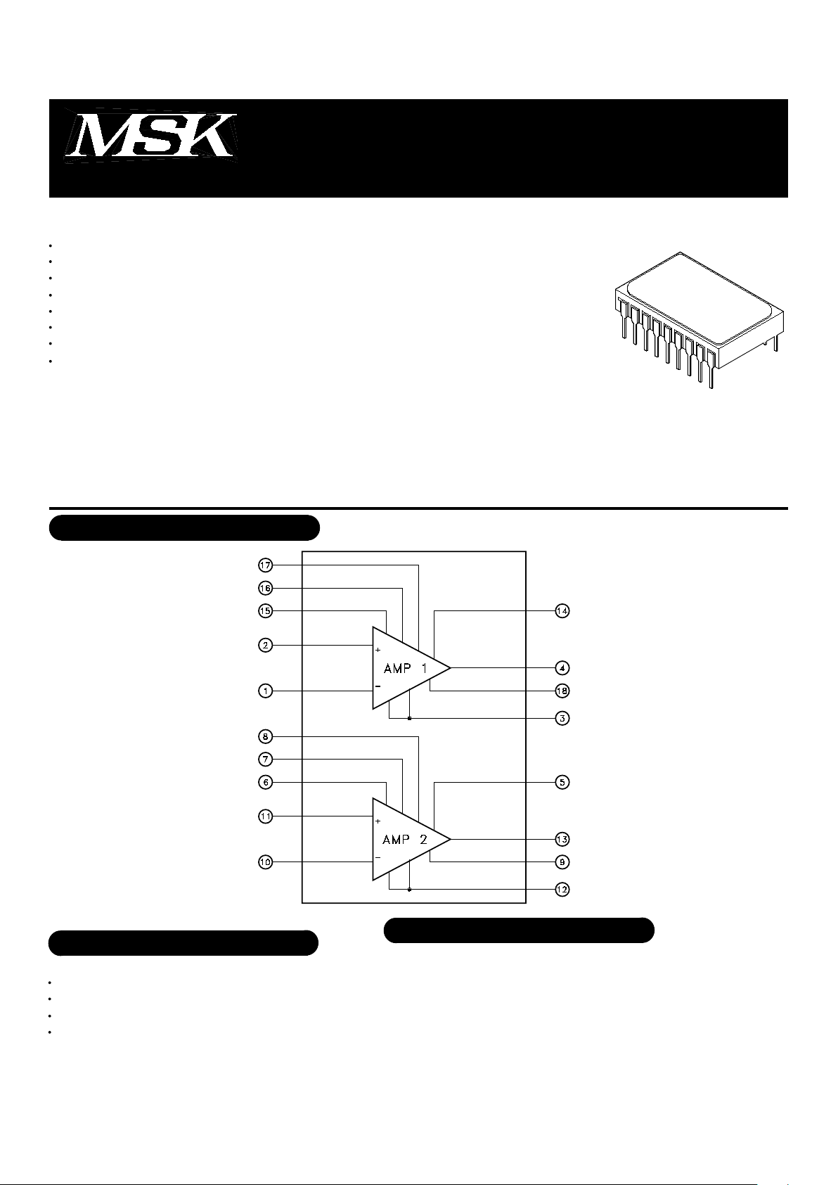
EQUIVALENT SCHEMATIC
TYPICAL APPLICATIONS
DESCRIPTION:
The MSK 101 is a dual high power monolithic MOSFET operational amplifier ideally suited for high power amplifi-
cation and magnetic deflection applications. With a total supply voltage rating of 150 volts and 5A of output current
available from each amplifier, the MSK 101 is also an excellent low cost choice for motor drive circuits. The MOSFET
output frees the MSK 101 from secondary breakdown limitations and power dissipation is kept to a minimum with a
typical quiescent current rating of only ± 8.0 mA total in class "C" mode. Power saving class "C" mode is enabled
by the user externally. The MSK 101 is packaged in a hermetically sealed 18 pin ceramic dip which has two external
compensation pins for each amplifier.
PIN-OUT INFORMATION
Current Sense 1
Amp 1 Comp 2
Amp 1 Comp 1
Quiescent Current Adjust 1
+Vcc 1
Output Drive 2
-Vcc 2
Non-Inverting Input 2
Inverting Input 2
Inverting Input 1
Non-Inverting Input 1
-Vcc 1
Output Drive 1
+Vcc 2
Quiescent Current Adjust 2
Amp 2 Comp 1
Amp 2 Comp 2
Current Sense 2
18
17
16
15
14
13
12
11
10
Operates In Class AB Or Class C Mode
Low Cost
High Voltage Operation : 150V
Low Quiescent Current : ± 8.0 mA Total Typ. In Class "C" Mode
High Output Current : 5A Min. Per Amplifier
No Second Breakdown
High Speed : 27V/µS Typ.
External Compensation For Optimum Gain-Bandwidth
1
2
3
4
5
6
7
8
9
Rev. A 7/00
1
MSK101
Page 2
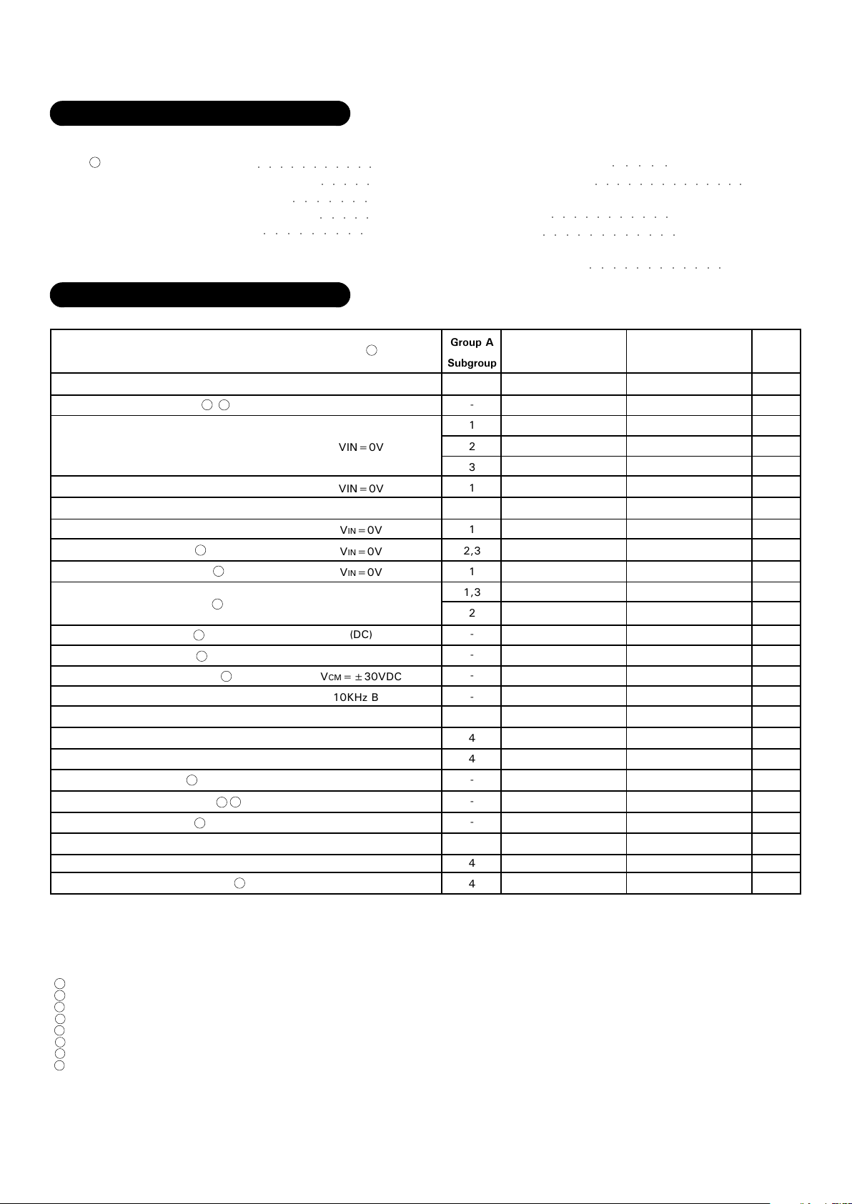
STATIC
Supply Voltage Range
Quiescent Current
Quiescent Current (Class 'C')
INPUT
Offset Voltage
Offset Voltage Drift
Offset Voltage vs ±Vcc
Input Impedance
Input Capacitance
Common Mode Rejection
Noise
OUTPUT
Output Voltage Swing
Output Current
Power Bandwidth
Settling Time to 0.1%
Capacitive Load
TRANSFER CHARACTERISTICS
Slew Rate
Open Loop Voltage Gain
Storage Temperature
Lead Temperature
Case Operating Temperature
(MSK101B)
(MSK101)
Thermal Resistance (DC)
Junction to Case
ABSOLUTE MAXIMUM RATINGS
150V
±5A
±16V
±Vcc
150°C
Total Supply Voltage
Output Current (within S.O.A.)
Input Voltage (Differential)
Input Voltage (Common Mode)
Junction Temperature
-65°C to +150°C
300°C
-55°C to +125°C
-40°C to +85°C
5.0°C/W
1
2
3
4
5
6
7
8
TST
TLD
TC
RTH
VCC
±IOUT
VIND
VIN
TJ
Unless otherwise noted CC=10pF, RC=1.0KΩ, ±VCC= ±50VDC and specifications apply to each amplifier.
Derate maximum supply voltage 0.5V/°C below TC=+25°C. No derating is needed above TC=25°C.
AV=-10V/V measured in false summing junction circuit.
Devices shall be capable of meeting the parameter, but need not be tested. Typical parameters are for reference only.
Industrial grade devices shall be tested to subgroups 1 and 4 unless otherwise requested.
Military grade devices ('B' suffix) shall be 100% tested to subgroups 1,2,3 and 4.
Subgroup 5 and 6 testing available upon request.
Subgroup 1,4 TC=+25°C
Subgroup 2,5 TC=+125°C
Subgroup 3,6 TA=-55°C
NOTES:
2
○○○○○○○○○○○
○○○○○
○○○○○
○○○○○○○○○○○○○○
○○○○○○○○○○○
○○○○○○○○○○○○
○○○○○○○○○○○○
○○○○○○○
○○○○○
○○○○○○○○○
Group A
Subgroup
-
1
2
3
1
1
2,3
1
1,3
2
-
-
-
-
4
4
-
-
-
4
4
VIN=0V
VIN=0V
VIN=0V
VIN=0V
VIN=0V
(DC)
VCM=±30VDC
10KHz BW
IOUT=±5A Peak
VOUT=MAX
VOUT=80VPP
10V Step
AV=+1V/V CC=68pF
CC=Open
F=15Hz
Typ.
±50
±30
±20
±35
4
±5
±10
±8
±20
-
10
5
106
10
±42
±5.5
66
2
-
27
106
1
Test Conditions
Max.
±75
±50
±45
±65
6
±10
±50
±15
±100
±50
-
-
-
-
-
-
-
-
-
-
-
Min.
±15
-
-
-
-
-
-
-
-
-
-
-
90
-
±40
±5
-
-
10
20
94
Min.
±15
-
-
-
-
-
-
-
-
-
-
90
-
±40
±5
-
-
10
20
94
Max.
±75
±50
-
-
6
±15
-
±15
±100
-
-
-
-
-
-
-
-
-
-
-
-
Typ.
±50
±30
-
-
4
±5
±10
±8
±20
-
10
5
106
10
±42
±5.5
66
2
-
27
106
Units
V
mA
mA
mA
mA
mV
µV/°C
µV/V
pA
nA
Ω
pF
dB
µVRMS
V
A
KHz
µS
nF
V/µS
dB
MSK101B
MSK101
Parameter
ELECTRICAL SPECIFICATIONS
4
4
3
4
4
4
4
4
4
4
4
2
±±
±
±
11
11
4
Input Bias Current VCM = 0V
2
Rev. A 7/00
Page 3

Input protection circuitry within the MSK 101 will clip differ-
ential input voltages greater than 16 volts. The inputs are also
protected against common mode voltages up to the supply rails
as well as static discharge. There are 300 ohm current limiting
resistors in series with each input. These resistors may be-
come damaged in the event the input overload is capable of
driving currents above 1mA. If severe overload conditions are
expected, external input current limiting resistors are recom-
mended.
CURRENT LIMIT (SEE TYPICAL CONNECTION DIAGRAM)
A value of current limit resistance can be calculated as fol-
lows:
Where:
RCL is the current limit resistor value
ICL is the current limit
0.05 ICL is the voltage dropped in the current limit path
across internal impedances other than the actual current
limit resistor
0.83 volts is the voltage drop that must be developed across
the current limit connections to activate the current limit
circuit
The maximum practical value of current limit resistance is 16
ohms. The current limit resistor will decrease available output
voltage swing in the following manner:
VR is the reduction in output voltage swing due to the current
limit resistor. It is recommended the user limit output current
to a value as close to the required output current as possible,
without clipping output voltage swing. Current limit will vary
with case temperature. Refer to the typical performance curves
to predict current limit drift. If current limit is not required
replace the resistor with a short.
SAFE OPERATING AREA (SOA)
The MOSFET output stage of this power operational ampli-
fier has two distinct limitations:
1. The current handling capability of the die metallization.
2. The junction temperature of the output MOSFET's.
NOTE: The output stage is protected against transient flyback.
However, for protection against sustained, high energy flyback,
external fast-recovery reverse biased diodes should be connected
from the output to ground.
V
R=IO RCL
*
R
CL=(0.83 - (0.05 ICL)) / ICL
*
*
STABILITY
The MSK 101 has sufficient phase margin when compen-
sated for unity gain to be stable with capacitive loads of at
least 10nF. However, it is recommended that the parallel sum
of the input and feedback resistor be 1000 ohms or less for
closed loop gains of ten or less to minimize phase shift caused
by the R-C network formed by the input resistor, feedback re-
sistor and input capacitance. The user can tailor the perfor-
mance of the MSK 101 to their application using the external
compensation pins. The graphs of small signal gain and phase
as well as the graphs of slew rate and power response demon-
strate the effect of various forms of compensation. The com-
pensation capacitor must be rated at 150 volts working voltage
if maximum power supply voltages are used. The compensa-
tion resistor and capacitor lead lengths must be kept as short
as possible to minimize spurious oscillations. A high quality
NPO capacitor is recommended for the compensation capaci-
tor. An effective method of checking amplifier stability is to
apply the worst case capacitive load to the output of the ampli-
fier and drive a small signal square wave across it. If overshoot
is less than 25%, the system will typically be stable.
INPUT PROTECTION
APPLICATION NOTES
TYPICAL CONNECTION DIAGRAM
CLASS "C" MODE
The user can enable class "C" mode by simply connecting pin
15 to pin 16 and pin 6 to pin 7. This connection will disable the
bias control network in the output stage of each amplifier.
Quiescent current will drop to ± 8 mA total typically and a
small amount of crossover distortion will appear on the output
waveforms. This mode of operation is recommended for switch-
ing type applications where distortion is not a critical specifica-
tion and quiescent power dissipation must be minimized. Dis-
connecting the pin 15 to pin 16 and pin 6 to pin 7 shorts will
enable the bias control network and the outputs will be biased
in class AB mode again. Pins 15 and 6 should be left uncon-
nected when using class AB mode. (Do not ground or pull high).
3
Rev. A 7/00
Page 4

TYPICAL PERFORMANCE CURVES
Rev. A 7/00
4
Page 5

Page 6

MECHANICAL SPECIFICATIONS
ESD TRIANGLE INDICATES PIN 1.
ALL DIMENSIONS ARE ±0.010 INCHES UNLESS OTHERWISE LABELED.
Rev. A 7/00
The information contained herein is believed to be accurate at the time of printing. MSK reserves the right to make
changes to its products or specifications without notice, however, and assumes no liability for the use of its products.
M.S. Kennedy Corp.
4707 Dey Road, Liverpool, New York 13088
Phone (315) 701-6751
FAX (315) 701-6752
www.mskennedy.com
MSK101
ORDERING INFORMATION
Screening Level
Part
Number
MSK101
MSK101B
Industrial
Military-Mil-PRF-38534
5
 Loading...