

Page 1
ISO 9001 CERTIFIED BY DSCC
HIGH SPEED, BUFFER
AMPLIFIER AMP
0002
M.S.KENNEDY CORP.
4707 Dey Road Liverpool, N.Y. 13088
FEATURES:
Industry Wide LH0002 Replacement
High Input Impedance-180KΩ Min
Low Output Impedance-10Ω Max
Low Harmonic Distortion
DC to 30 MHz Bandwidth
Slew Rate is Typically 400 V/µS
Operating Range from±5V to ±20V
Available to DSCC SMD5962-7801301XC
MIL-PRF-38534 CERTIFIED
(315) 701-6751
DESCRIPTION:
The MSK 0002 is a general purpose current amplifier. It is the industry wide replacement for the LH0002. The
device is ideal for use with an operational amplifier in a closed loop configuration to increase current output. The MSK
0002 is designed with a symmetrical output stage that provides low output impedances to both the positive and
negative portions of output pulses. The MSK 0002 is packaged in a hermetic 8 lead low profile T0-5 header and is
specified over the full military temperature range.
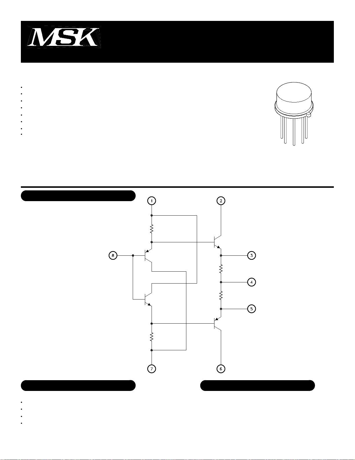
EQUIVALENT SCHEMATIC
TYPICAL APPLICATIONS
High Speed D/A Conversion
30MHz Buffer
Line Driver
Precision Current Source
PIN-OUT INFORMATION
V1+
1
V2+
2
E3
3
Output
4
1
5
E4
6
V2-
7
V1-
8
Input
Rev. - 10/00
Page 2
ABSOLUTE MAXIMUM RATINGS
Supply Voltage
±VCC
Input Voltage
VIN
Power Dissipation
Pd
Case Operating Temperature
Tc
(MSK 0002H)
(MSK 0002)
○○○○○○○○○○○○○○○○
○○○○○○○○○○○○○○○○
○○○○○○○○○○○○○
○○○○○○○○○○
○○○○○○○○○○
ELECTRICAL SPECIFICATIONS
±22V
±22V
600mW
-55°C to +125°C
-40°C to +85°C
TST
Storage Temperature Range
TLD
Lead Temperature Range
(10 Seconds)
TJ
Junction Temperature
θjC
Thermal Resistance
-65°C to +150°C
○○○○○○○○○○
○○○○○○○○○○○○
○○○○○○○○○○○○○
+300°C
+175°C
40°C/W
Parameter
Quiescent Current
Input Offset Current
Input Offset Voltage
Input Impedance
Output Impedance
3
3
Output Voltage Swing
Voltage Gain
2
Rise Time
Test Conditions
1
VIN=0V
RS=10KΩ RL=1.0KΩ
RS=10KΩ RL=1.0KΩ
RS=300Ω RL=1.0KΩ
VIN=1.0VRMS RS=200KΩ
RL=1KΩ f=1.0KHz
VIN=1.0VRMS Rs=10KΩ
RL=50Ω f=1.0KHz
VIN=±12Vp RL=1.0KΩ
f=1.0KHz
VIN=±10Vp RL=100Ω
+VCC=±15V f=1.0KHz
VIN=3.0VPP f=1.0KHz
RS=10KΩ RL=1.0KΩ
VOUT=2.5VPP f=10KHz
RS=100Ω RL=50Ω
Group A
Subgroup
1
1
2,3
1
2,3
4
4
4
4
4
5,6
4
MSK 0002H
Min. Typ. Max.
±6.3
±2
±2
±6
±10
-
-
±11
-
0.97
-
8
±10
±10
±10
±30
±30
10
12
-
-
-
-
-
180
-
±10
±9.5
0.95
0.95
-
4
MSK 0002
Min. Typ. Max.
-
-
-
-
-
-
180
-
-
±10
-
±9.5
0.95
-
-
-
-
±6.3
±2
-
±6
-
-
-
±11
-
0.97
-
8
±10
±10
-
±30
-
-
10
-
-
-
-
12
Units
mA
µA
µA
mV
mV
KΩ
Ω
Vp
Vp
V/V
V/V
nS
NOTES:
1
Unless otherwise specified ±V
2
Subgroups 5 & 6 shall be tested as part of device initial characterization and after design
and process changes. Parameter shall be guaranteed to the limits specified for subgroups
5 & 6 for all lots not specifically tested.
3
Devices shall be capable of meeting the parameter, but need not be tested.
4
Subgroup 1,4 TA=TC=+25°C
Subgroup 2,5 TA=TC=+125°C
Subgroup 3,6 TA=TC=-55°C
CC=±12VDC
Rev. - 10/002
Page 3

APPLICATION NOTES
HEAT SINKING
To determine if a heat sink is necessary for your application
and if so, what type, refer to the thermal model and governing
equation below.
Thermal Model:
R
ΘSA = ((TJ - TA)/PD) - (RΘJC) - (RΘCS)
= ((125°C - 80°C) / 0.36W) - 40°C/W - 0.15°C/W
= 125 - 40.15
= 84.9°C/W
This heat sink in this example must have a thermal resistance
of no more than 84.9°C/W to maintain a junction temperature
of no more than +125°C.
Typical Applications:
Governing Equation:
TJ=PD X (RΘJC +RΘCS +RΘSA) +TA
Where
TJ=Junction Temperature
PD=Total Power Dissipation
RΘJC=Junction to Case Thermal Resistance
RΘCS=Heat Sink to Ambient Thermal Resistance
TC=Case Temperature
TA=Ambient Temperature
TS=Sink Temperature
Example:
This example demonstrates a worst case analysis for the buffer
output stage. This occurs when the output voltage is 1/2 the
power supply voltage. Under this condition, maximum power
transfer occurs and the output is under maximum stress.
Conditions:
VCC= ±12VDC
Vo= ±6Vp Sine Wave, Freq. = 1KHz
RL= 100Ω
For a worst case analysis we will treat the ±6Vp sine wave as
an 6 VDC output voltage.
1.) Find Driver Power Dissipation
PD= (Vcc-Vo) (Vo/RL)
= (12V-6V) (6V/100Ω)
= 360mW
2.) For conservative design, set TJ=+125°C Max.
3.) For this example, worst case TA=+80°C
4.) RΘJC = 40° C/W from MSK 0002H Data Sheet
5.) RΘCS = 0.15° C/W for most thermal greases
6.) Rearrange governing equation to solve for RΘSA
Rev. - 10/003
Page 4

TYPICAL PERFORMANCE CURVES
4
Rev. - 10/00
Page 5

MECHANICAL SPECIFICATIONS
ALL DIMENSIONS ARE ±0.010 INCHES UNLESS OTHERWISE LABELED
ORDERING INFORMATION
Part
Number
MSK0002
MSK0002H
7801-301XC
M.S. Kennedy Corp.
4707 Dey Road, Liverpool, New York 13088
Phone (315) 701-6751
FAX (315) 701-6752
www.mskennedy.com
The information contained herein is believed to be accurate at the time of printing. MSK reserves the right to make
changes to its products or specifications without notice, however, and assumes no liability for the use of its products.
Screening Level
Industrial
Military-Mil-PRF-38534
DSCC-SMD
Rev. - 10/005
 Loading...