

Page 1
MSD601
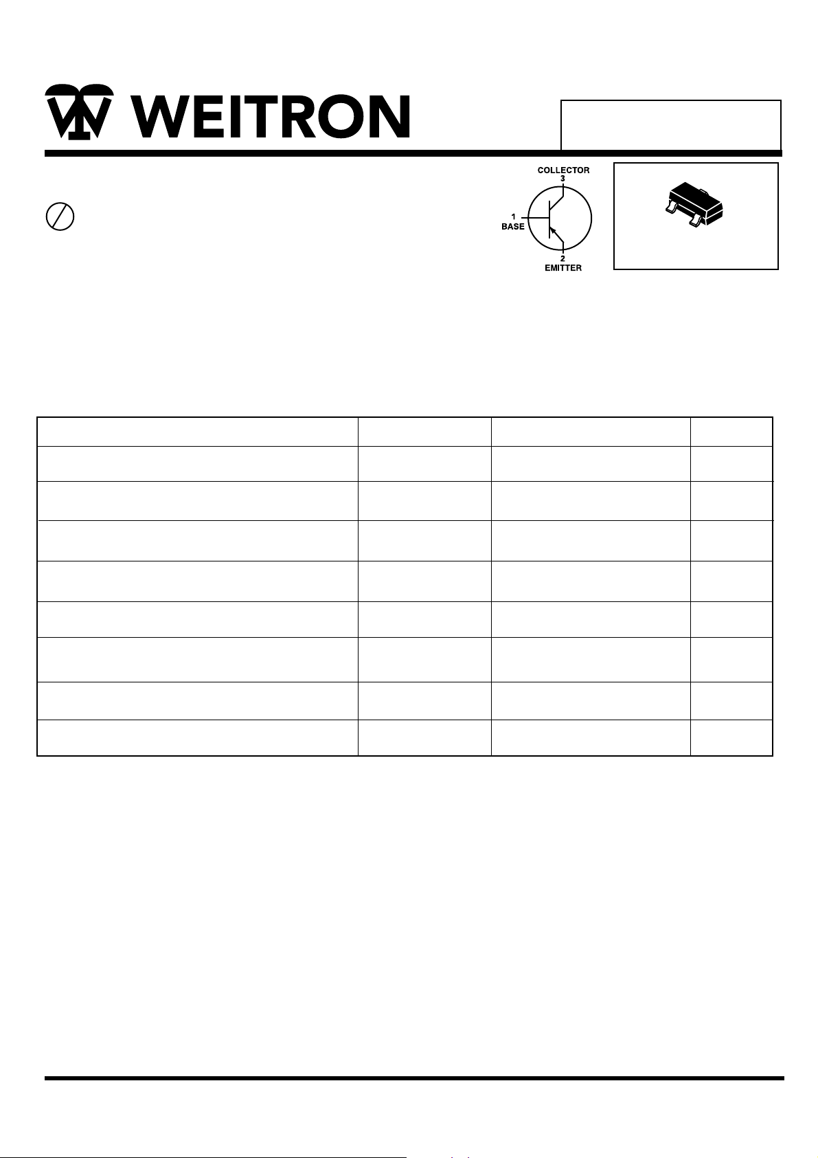
NPN General Purpose Transistors
P b
Lead(Pb)-Free
1
3
2
SOT-23
MAXIMUM RATINGS(Ta=25°C)
Rating
Collector-Emitter Voltage
Collector-Base Voltage
Emitter-Base Voltage
Collector Current - Continuous mA
Symbol
V
CEO
V
CBO
V
EBO
I
C
Value Unit
50
60
7.0
100
V
V
V
T
I
C(P)
P
T
stg
D
j
Collector Current - Peak mA
Total Device Dissipation
TA=25°C
Junction Temperature
Storage Temperature
200
0.2
+150
-55 to +150
mW
°C
°C
WEITRON
http://www.weitron.com.tw
1/6 18-Sep-06
Page 2
MSD601
ELECTRICAL CHARACTERISTICS
Characteristics Symbol Min MaxTyp Unit
Collector-Emitter Breakdown Voltage
IC = 2.0mA, IE = 0A
Collector-Base Breakdown Voltage
IC = 10µA, IB = 0A
Emitter-Base Breakdown Voltage
IE= 10µA, IC=0
Collector Cutoff Current
VCB = 45V, IC = 0A
Emitter Cutoff Current
VEB = 10V, IC = 0A
ON CHARACTERISTICS
V
(BR)CEO
V
(BR)CBO
V
(BR)EBO
I
CBO
I
CEO
50
60
7.0
-
-
-
-
-
-
-
-
-
-
0.1
0.1
V
V
V
µA
µA
Collector-Emitter Saturation Voltage
IC = 100mA, IB = 10mA
DC Current Transfer Ration
VCE =2.0V, IC = 100mA
1.Pulse Test : Pulse Width ≤ 300µs, D.C. ≤ 2%
CLASSIFICATION h
1
@VCE = 10V, IC = 2.0mA
FE
Rank
Range
Marking
V
CE(sat)
h
FE
-
R
-
-90
S
210-340 290-460
YR YS
0.5
-
V
WEITRON
http://www.weitron.com.tw
2/6
18-Sep-06
Page 3
MSD601
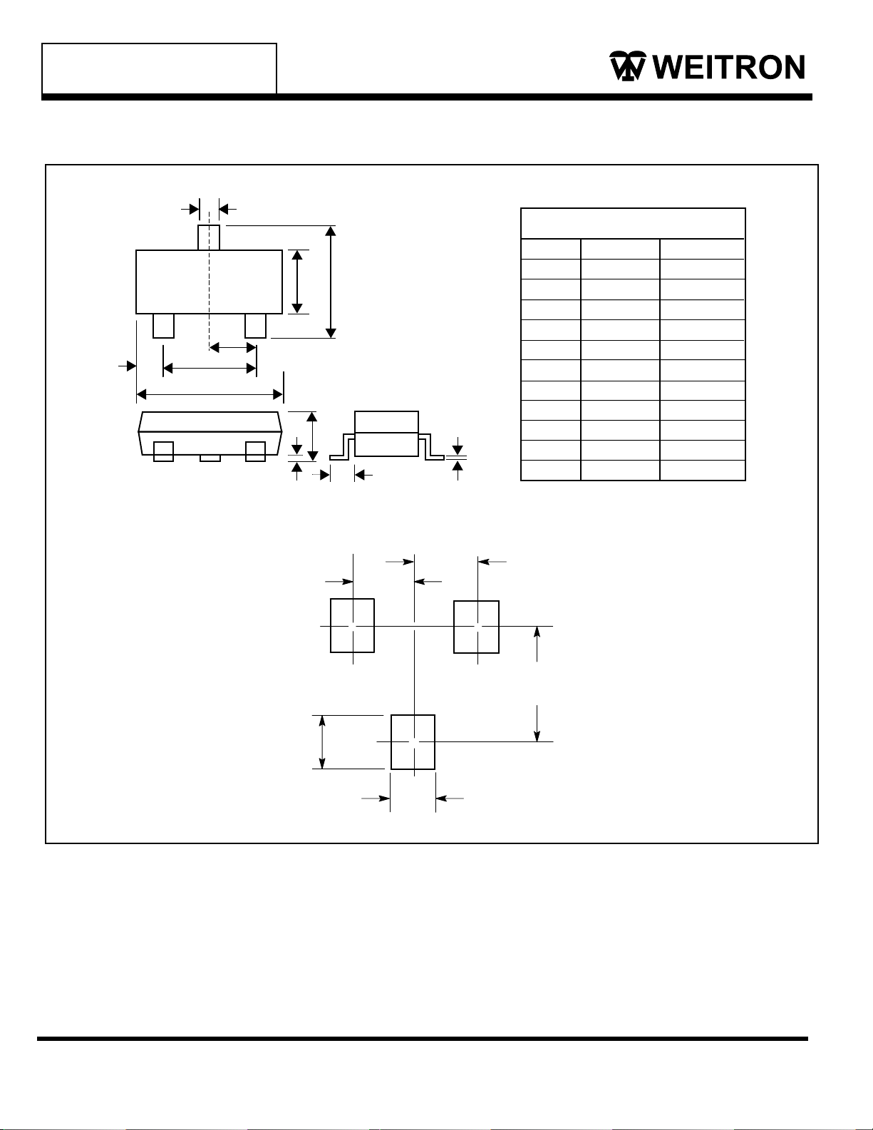
SOT-23 Outline Dimension
A
B
TOP VIEW
D
E
G
H
C
K
L
J
M
Dim
A
B
C
D
E
G
H
J
K
L
M
SO
Min
0.35
1.19
2.10
0.85
0.46
1.70
2.70
0.01
0.89
0.30
0.076
Unit:mm
T-23
Max
0.51
1.40
3.00
1.05
1.00
2.10
3.10
0.13
1.10
0.61
0.25
0.95
0.9
0.95
2.0
0.8
WEITRON
http://www.weitron.com.tw
3/6
18-Sep-06
Page 4
MSD601
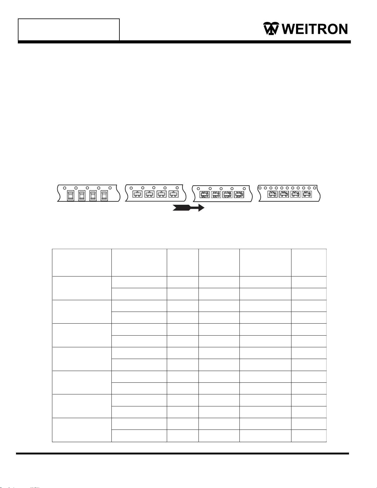
Tape & Reel and Packaging Specifications for
Small-Signal
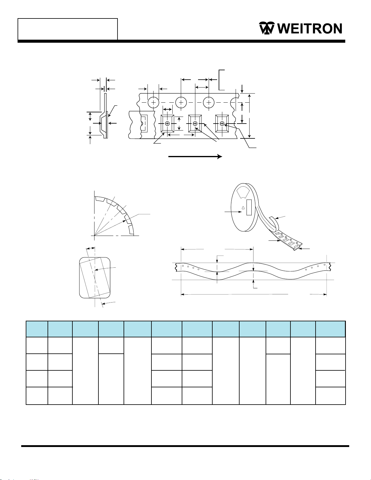
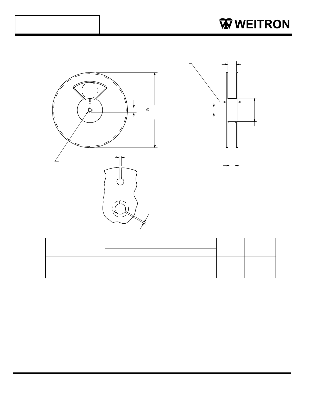
Embossed Tape and Reel is used to facilitate automatic pick and place equipment feed requirements. The tape is used as the
shipping container for various products and requires a minimum of handling. The antistatic/conductive tape provides a secure
cavity for the product when sealed with the “peel–back” cover tape.
• Two Reel Sizes Available (7"and 13",)
• Used for Automatic Pick and Place Feed Systems
• Minimizes Product Handling
• EIA 481, –1, –2
Use the standard device title and add the required suffix as listed in the option table below (Table 1). Note that the individual
reels have a finite number of devices depending on the type of product contained in the tape. Also note the minimum lot size is
one full reel for each line item, and orders are required to be in increments of the single reel quantity.
SOD-323
8 mm
Transistors, FETs and Diodes
• SOT–23, SC–70/SOT–323,
SC–89, SC–88/SOT–363,SC–88A/SOT–353,
SOD–323, SOD-523 in 8 mm Tape
SC-59, SC-70, SC-75,SOT-23
8 mm
SC-88, SOT-363
T1 Orientation
8 mm
Direction of Feed
SC-88A, SOT-353
T1 Orientation
8 mm
Typical Reel Orientations
Table 1. EMBOSSED TAPE AND REEL ORDERING INFORMATION
Package
3
SOT–2
SC–70/SOT–32
SC–89
SC–88/SOT-36
SC–88A/SOT-35
SOD-32
SOD-52
3
3
Tape Width Pitch Reel Size Devices Per Reel Device
(mm
3
3
3
) mm mm(inch) and Minimum Suffix
Order Quantity
8
8
8
8
8
8
8
8
8
8
8
8
8
8
4
4
4
4
4
4
4
4
4
4
4
4
4
4
178
330
178
330
178
330
178
330
178
330
178
330
178
330
(7)
(13)
(7)
(13)
(7)
(13)
(7)
(13)
(7)
(13)
(7)
(13)
(7)
(13)
3,000
10,000
3,000
10,000
3,000
10,000
3,000
10,000
3,000
10,000
3,000
10,000
3,000
10,000
WEITRON
http://www.weitron.com.tw
4/6
18-Sep-06
Page 5
MSD601
EMBOSSED TAPE AND REEL DATA FOR DISCRETES
CARRIER TAPE SPECIFICATIONS
K
t
Top Cover
Tape
#
Note 1
Bending
K
0
0
Radius
Typical Component
Center Line
Cavity
B
1
FOR MACHINE REFERENCE ONLY
INCLUDING DRAFT AND RADII
CONCENTRIC AROUND B
10
°
Maximum Component Rotation
D
Embossment
User Direction of Feed
0
R Min
Tape and Components
Shall
Pass Around Radius “R”
Damage
Without
P
0
A
0
B
0
P
Barcode Label
10 Pitches Cumulative Tolerance on Tape
±0.2 mm
P
2
E
F
W
Center Lines
of Cavity
100 mm
Embossed Carrier
1 mm Max
D1
For Components
2.0 mm x 1.2 mm and Larger
Top Cover Tape Thickness
0.10
mm Max.
Tape
Embossment
1 mm Max
Typical Component
Line
Center
Allowable
(Top View)
Camber To Be 1 mm/100 mm Nonaccumulative Over 250 mm
Camber
250
DIMENSIONS
Max
B
Size
8mm
12mm
16mm
24mm
Metric dimensions govern - English are in parentheses for reference only.
NOTE 1: A 0 , B 0 , and K 0 are determined by component size. The clearance between the components and the cavity must be within
NOTE 2: the component cannot rotate more than 10 owithin the determined cavity.
NOTE 3: If B1 exceeds 4.2 mm for 8 mm embossed tape, the tape may not feed through all tape feeders.
http://www.weitron.com.tw
1
#(Note 2)
D D
4.55 mm
-0.0
8.2 mm
12.1 mm
20.1 mm
.05 mm min. to.50 mm max.,
WEITRON
1
1.0 Min
1.5 mm Min
E F K P
1.75±0.1 mm
3.5±0.05 mm
5.5±0.05 mm
7.5±0.10 mm
11.5±0.1 mm
2.4 mm Max
6.4 mm Max
7.9 mm Max
11.9 mm Max
5/6
0
P
2.0±0.1 mm4.0±0.1 mm1.5+0.1 mm
R Min T Max W Max
2
30 mm
0.6 mm25 mm
mm
8.3 mm
12±0.3 mm
16.3 mm
24.3 mm
18-Sep-06
Page 6
MSD601
EMBOSSED TAPE AND REEL DATA FOR DISCRETES
DE
TAIL A
20.2
MIN
330.0
MAX
3.5 to 2.5
TAPE START SLOT
(MEASURED
AT HUB)
D
13.2 to 12.8
HOLE)
(ARBOR
E
(MEASURED
EDGE)
OUTER
A
DIA)
(HUB
C
(MEASURED
HUB)
INNER
AT
AT
1.6
DETAIL A
Reel
Diameter
Tape
Size
Min Max Min Max
178.0 8.0 50.0
330.0 8.0 50.0 8.4 9.9 14.4 10.9
A C D
(Max)
- 8.4 9.9 14.4 10.9
-
E
(Max)
Reel Dimensions
Metric Dimensions Govern - English are in parentheses for reference only
Storage Conditions
Temperature: 5 to 40 Deg.C (20 to 30 Deg. C is preferred) Humidity: 30 to 80 RH (40 to 60 is preferred )
Recommended Period: One year after manufacturing (This recommended period is for the soldering
condition only. The characteristics and reliabilities of the products are not restricted to this limitation)
WEITRON
http://www.weitron.com.tw
6/6
18-Sep-06
 Loading...