

Page 1

E2C0031-27-Y2
¡ Semiconductor
This version: Nov. 1997
Previous version: Jul. 1996
MSC7165¡ Semiconductor
MSC7165
16-Bit Grid Driver with 4 to 16-Decoder
GENERAL DESCRIPTION
The MSC7165 is a driver IC designed to directly drive the grids of a vacuum fluorescent display
tube.
Since this IC has a built-in 4 to 16-line decoder and 16 output circuits, a single device of MSC7165
can replace a set of the following three: two devices of either MSL915 or MSL917 and one device
of either MSM4514 or MSM74HC4514.
Setting the DUTY pin to the "L" level makes all driver outputs go "L". Blanking can be set using
this function.
FEATURES
• Logic supply voltage : 5V
• Driver supply voltage : –60V
• Driver output current
I
: –40mA
OH
I
: 1mA
OL
• Can be connected directly to VFD without a pull-down resistor
• Built-in 4 to 16-line decoder
• Brightness can be adjusted by the DUTY pin
• Package:
24-pin plastic SOP (SOP24-P-430-1.27-K) (Product name: MSC7165GS-K)
1/8
Page 2
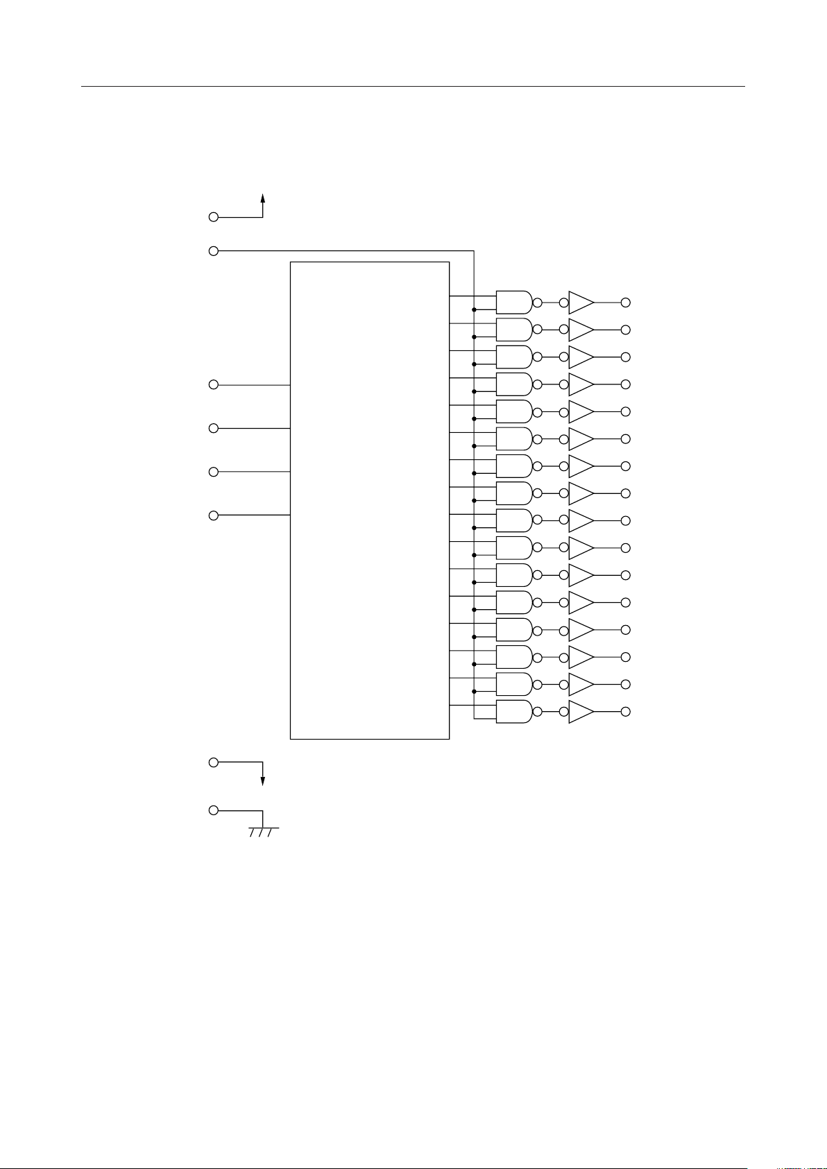
BLOCK DIAGRAM
V
DD
DUTY
MSC7165¡ Semiconductor
SEL 0
SEL 1
SEL 2
SEL 3
4 to 16
DECODER
S 1
S 2
S 3
S 4
S 5
S 6
S 7
S 8
S 9
S 10
S 11
S 12
S 13
S 14
S 15
S 16
GRID 1
GRID 2
GRID 3
GRID 4
GRID 5
GRID 6
GRID 7
GRID 8
GRID 9
GRID 10
GRID 11
GRID 12
GRID 13
GRID 14
GRID 15
GRID 16
V
DISP(–)
V
ss
2/8
Page 3
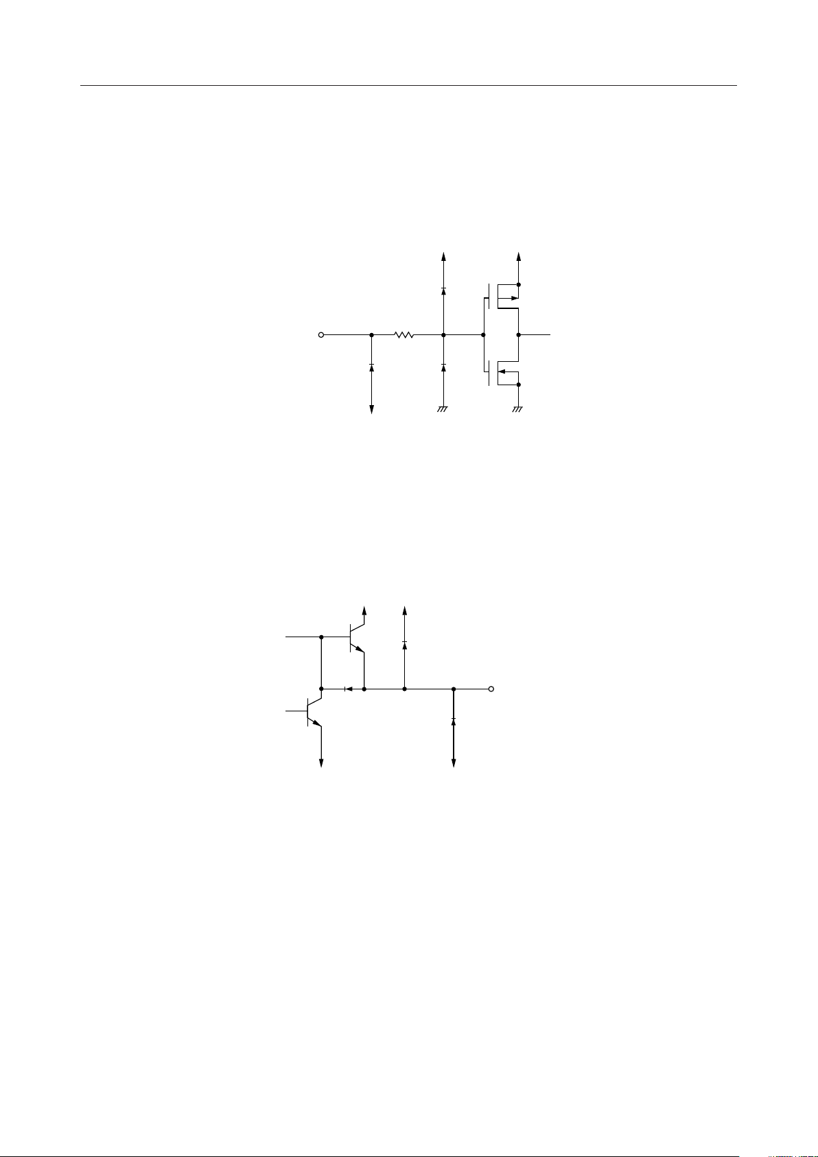
INPUT AND OUTPUT CONFIGURATION
Schematic Diagrams of Logic Portion Input Circuit
MSC7165¡ Semiconductor
Input
V
DISP(–)
Schematic Diagram of Driver Output Circuit
V
V
DD
DD
V
DD
V
SS
V
DD
V
SS
V
DISP(–)
V
DISP(–)
Output
3/8
Page 4
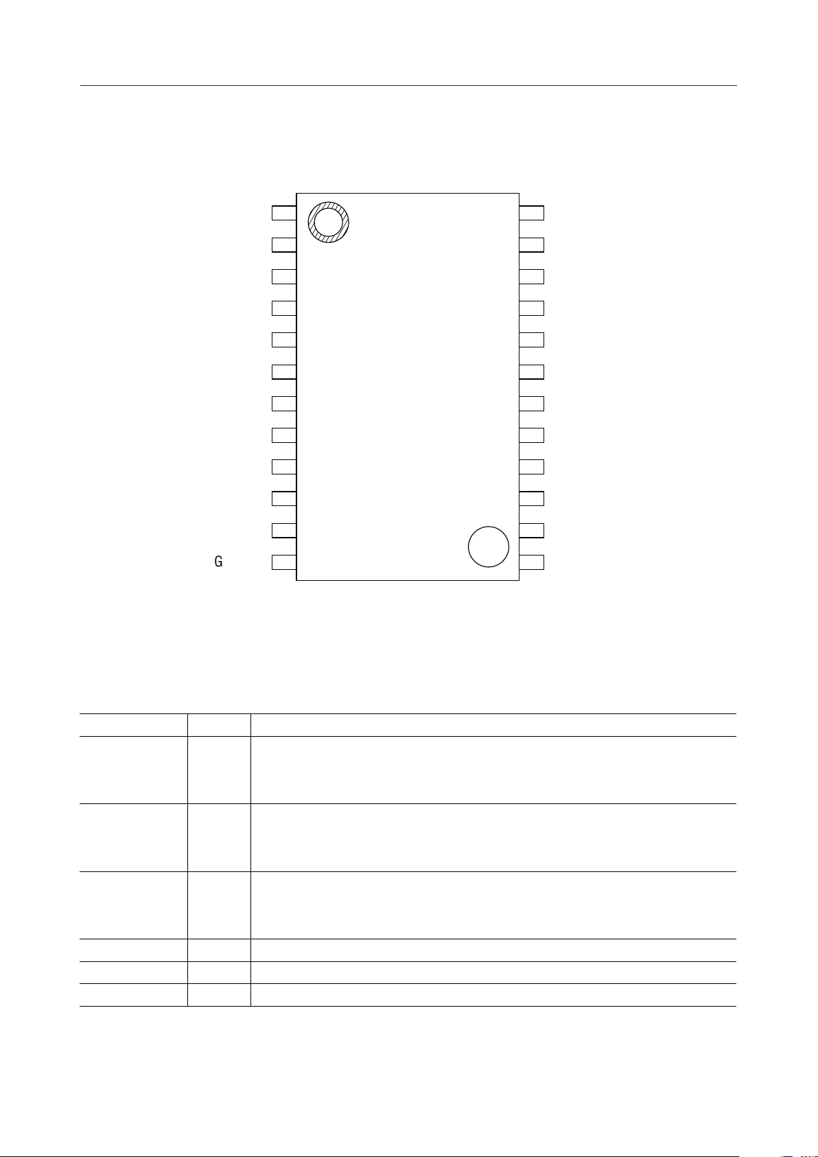
PIN CONFIGURATION (TOP VIEW)
MSC7165¡ Semiconductor
GRID 1
GRID 2
GRID 3
GRID 4
GRID 5
GRID 6
GRID 7
GRID 8
GRID 9
GRID 10
GRID 11
GRID 12
10
11
12
1
2
3
4
5
6
7
8
9
24
23
22
21
20
19
18
17
16
15
14
13
V
DISP(–)
SEL 0
SEL 1
SEL 2
SEL 3
DUTY
V
SS
V
DD
GRID 13
GRID 14
GRID 15
GRID 16
24-Pin Plastic SOP
PIN DESCRIPTIONS
Symbol Type
SEL0-3 I
IDUTY
GRID1-16 O
V
DISP(–)
V
DD
V
SS
—
—
—
Description
4- to 16-line decoder input pins
The input 4-bit binary signals are converted into hexadecimal signals, then output
through driver output pins.
Duty control signal input pin
Setting this pin to "L" makes all driver outputs go "L", so this pin can be used for
brightness control.
High withstand voltage driver output pins for driving fluorescent display tube
These pins can be connected directly to the grid of fluorescent display tube.
No pull-down resistor is required.
Power supply pin for the fluorescent display tube driver circuit
Logic power supply pin
Ground pin
4/8
Page 5
MSC7165¡ Semiconductor
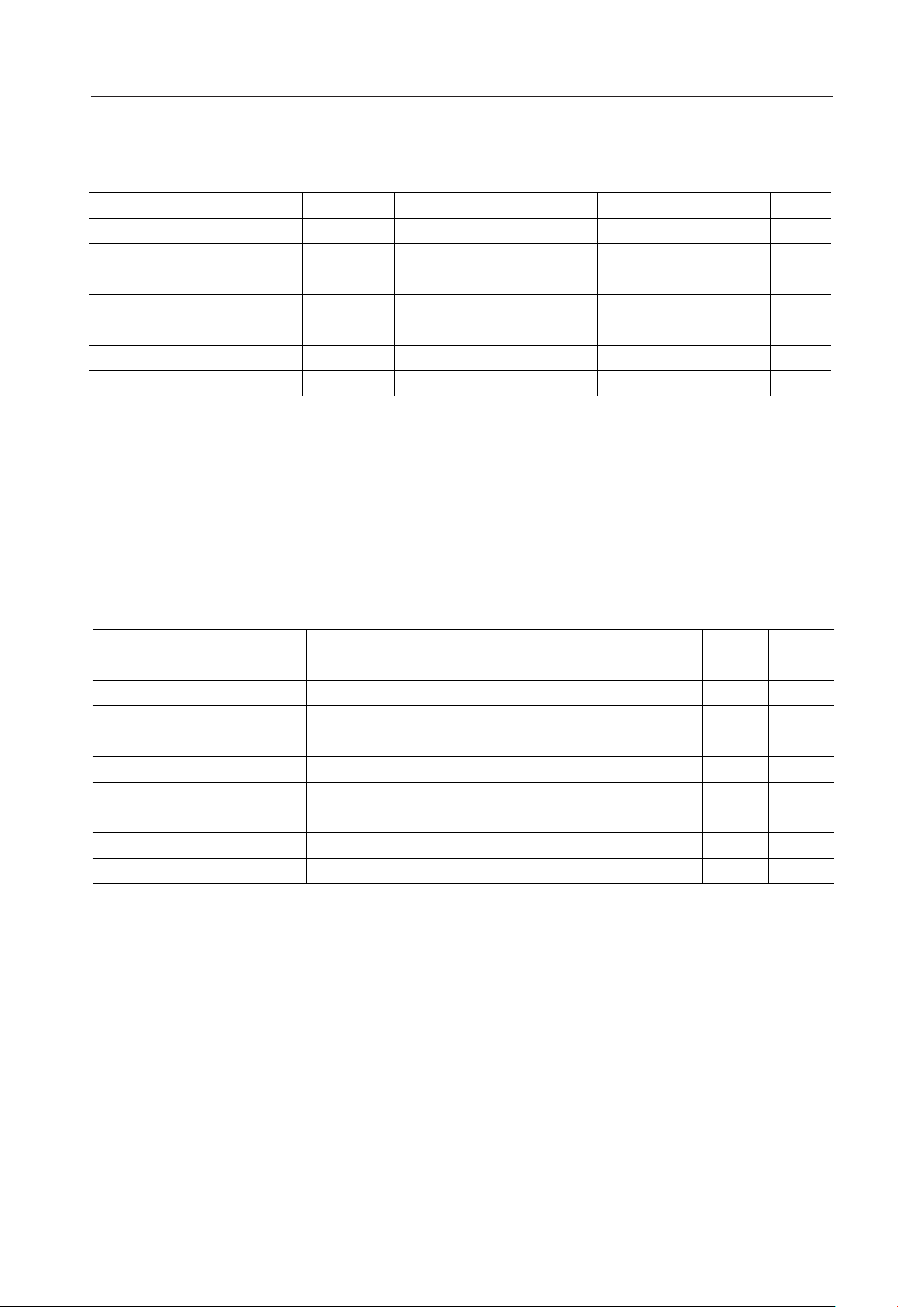
ABSOLUTE MAXIMUM RATINGS
Parameter Symbol Condition Rating Unit
Logic Supply Voltage V
DD
Applied to logic supply pin –0.3 to +6.5 *1
*1
Driver Supply Voltage
Input Voltage
Power Dissipation
Package Thermal Resistance
Storage Temperature
V
DISP(–)
V
P
R
T
STG
IN
D
j–a
*1 The maximum supply voltage for V
Applied to driver supply pin –70 to V
DD
Applied to all input pins –0.3 to VDD+0.3 *1
Ta<25°C 790
=
— 158 *3
—
SS
–55 to +150
*2
*2 Permanent damage to the device may be caused if the voltage is supplied over the absolute
maximum rating value.
*3 Thermal resistance of the package (between junction and atmosphere)
The junction temperature (T
Tj=P¥R
+Ta (P: Maximum power consumption of IC)
j–a
) given by the equation indicated below should not exceed 150°C.
j
V
V
V
mW
°C/W
°C
RECOMMENDED OPERATING CONDITIONS
Parameter Symbol Condition Min. Max.
Logic Supply Voltage V
V
DISP(–)
High Level Input Voltage
Low Level Input Voltage
High Level Output Current
Low Level Output Current
Operating Temperature
Input Pulse Rise time
Input Pulse Fall Time
DD
V
IH
V
IL
I
OH
I
OL
T
op
t
r
t
f
Applied to logic supply pin 4.5 5.5
Applied to driver supply pin –60 –5Driver Supply Voltage
Applied to all input pins 3.1
Applied to all input pins 1.7
Applied to all driver output pins
Applied to all driver output pins
Applied to all input pins 1.0
Applied to all input pins 1.0 µs
—
—
—
—
—
–40
1.0
–40 85
—
—
Unit
V
V
V
V
mA
mA
°C
µs
5/8
Page 6
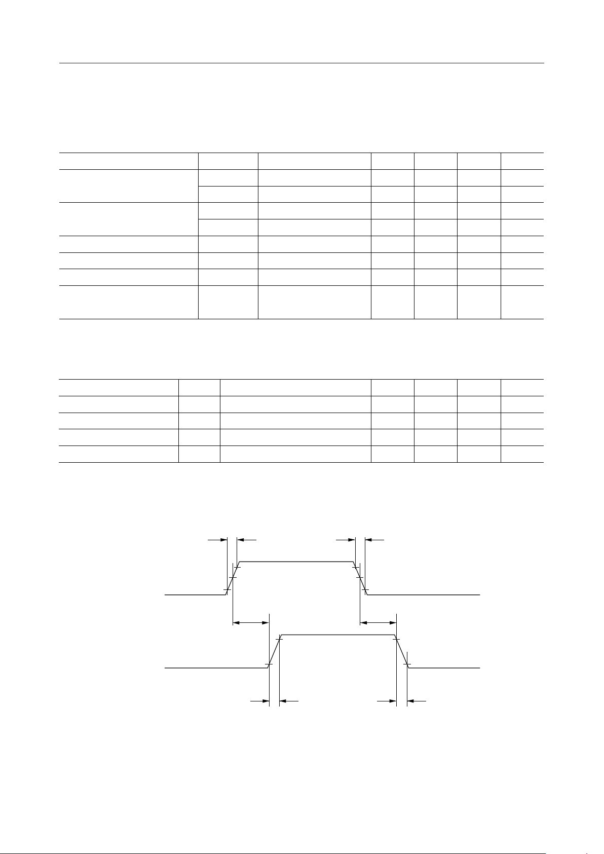
ELECTRICAL CHARACTERISTICS
DC Characteristics
MSC7165¡ Semiconductor
=4.5 to 5.5V, V
(V
DD
=–60 to –5V, Ta=–40 to +85°C)
DISP(–)
Parameter Symbol Condition Min. Typ. Max. Unit
Logic Supply Voltage I
Driver Supply Voltage I
I
High Level Input Current I
Low Level Input Current I
High Level Output Voltage V
Low Level Output Voltage V
DD1
I
DD2
DISP1
DISP2
IH
IL
OH
OL
No load, 1 output H — 6.0 mA
No load, DUTY=L — 6.0 mA
No load, 1 output H –6.0 — mA
No load, DUTY=L –6.0 — mA
—
—
——±1µA
——±1µA
IOH=–40mA VDD–4 — — V
IOL=1mA — — V
AC Characteristics
(VDD=4.5 to 5.5V, V
Parameter Symbol Condition Min. Typ. Max. Unit
Delay Time L to H t
Transient Time L to H
Delay Time H to L
Transient Time H to L 2.0
DLH
t
TLH
t
DHL
t
THL
CL=10pF, See figure below — 1.5 µs
CL=10pF, See figure below — 4.0 µs
CL=10pF, See figure below — 1.0 µs
CL=10pF, See figure below — 4.0 µs
=–60 to –5V, Ta=–40 to +85°C)
DISP(–)
—
—
—
—
0.5
2.0
0.3
DISP(–)
+2.5
V
DUTY
SELn
GRIDn
10%
t
90%
50%
t
DLH
10%
r
t
f
90%
50%
10%
t
DHL
90%
90%
10%
t
TLH
t
THL
6/8
Page 7
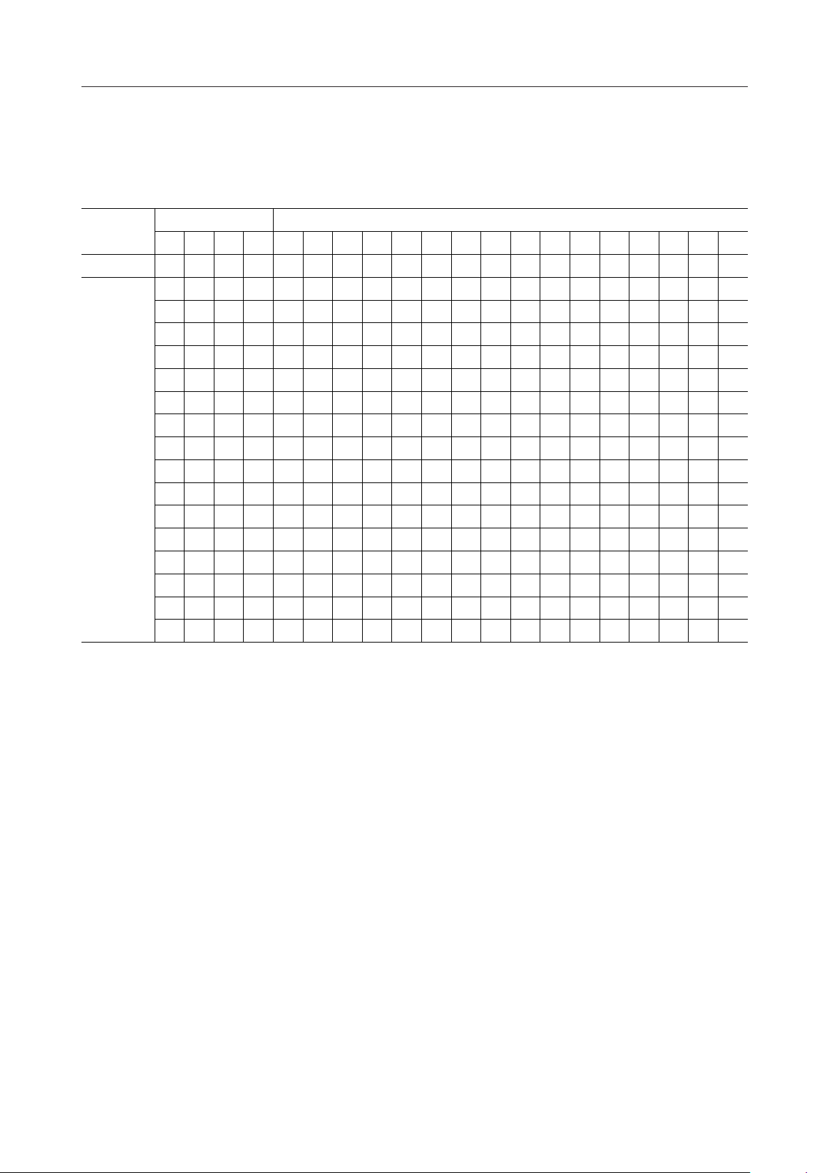
FUNCTIONAL DESCRIPTION
Function Table
MSC7165¡ Semiconductor
DUTY
L
H
SEL GRID
012312345678910111213141516
XXXXLLLLLLLLLLLLLLLL
LLLL
HLLL
LHLL
HHL L
LLHL
HLHL
LHHL
HHHL
LLLH
HLLH
LHLH
HHLH
LLHH
HLHH
LHHH
HHHH
HLLLLLLLLLLLLLLL
LHLLLLLLLLLLLLLL
LLHLLLLLLLLLLLLL
LLLHLLLLLLLLLLLL
LLLLHLLLLLLLLLLL
LLLLLHLLLLLLLLLL
LLLLLLHLLLLLLLLL
LLLLLLLHLLLLLLLL
LLLLLLLLHLLLLLLL
LLLLLLLLLHLLLLLL
LLLLLLLLLLHLLLLL
LLLLLLLLLLLHLLLL
LLLLLLLLLLLLHLLL
LLLLLLLLLLLLLHLL
LLLLLLLLLLLLLLHL
LLLLLLLLLLLLLLLH
7/8
Page 8
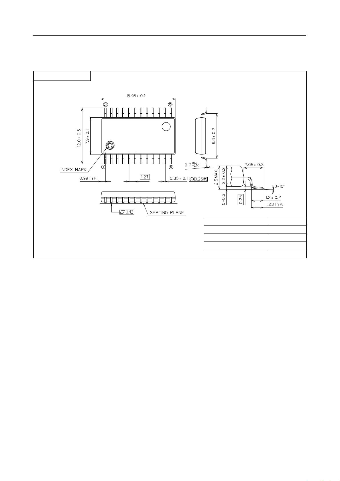
PACKAGE DIMENSIONS
SOP24-P-430-1.27-K
Mirror finish
MSC7165¡ Semiconductor
(Unit : mm)
Package material
Lead frame material
Pin treatment
Solder plate thickness
Package weight (g)
Epoxy resin
42 alloy
Solder plating
5 mm or more
0.58 TYP.
Notes for Mounting the Surface Mount Type Package
The SOP, QFP, TSOP, SOJ, QFJ (PLCC), SHP and BGA are surface mount type packages, which
are very susceptible to heat in reflow mounting and humidity absorbed in storage.
Therefore, before you perform reflow mounting, contact Oki’s responsible sales person for the
product name, package name, pin number, package code and desired mounting conditions
(reflow method, temperature and times).
8/8
 Loading...