

Page 1

E2C0029-27-Y4
¡ Semiconductor MSC7128-xx
¡ Semiconductor
This version: Nov. 1997
Previous version: Jul. 1996
MSC7128-xx
5 ¥ 7-Dot Character ¥ 16-Digit Display Controller/Driver
GENERAL DESCRIPTION
The MSC7128-xx is a general purpose display controller for vacuum fluorescent display tube.
The MSC7128-xx drives displays with up to 35 anodes (dots) and up to 16 grids (characters) plus
a cursor.
The controller accepts command and display data input words on a clocked serial input line.
Commands control the on/off duty cycle, starting character position, number of characters to
display and display modes (PLA mode and Lamp Test mode). An internal PLA-type character
generator provides character decoding and dot pattern generation for the full 128 characters.
A 35 ¥ 128-bit PLA (ROM) code is programmable.
FEATURES
• Logic supply voltage (VDD) :+5V
• VF driver supply voltage (VEE) :–55V
• Driver output current
– VF grid driver :–30mA
– VF anode driver :–2mA
– VF cursor driver :–10mA
• Direct drive capability for vacuum fluorescent display (no pull-down resistor is required)
• Built-in oscillation circuit
• Built-in power-on-reset circuit with external C
• Serial host interface (data in, clock, chip select)
• Serial data input for 8-bit control and display data words
• Command functions
– On/off duty cycle : 0/16 to 15/16
– Character display position : 0 to 15
– Number of display digits :1 to 16
– Display modes : PLA mode, and Lamp Test mode
• Built-in 35 x 128-bit PLA-type character generator
– Character font :5 ¥ 7
– Number of characters :128
– Programmable PLA code
• Package options:
64-pin plastic SDIP (SDIP64-P-750-1.78) (Product name : MSM7128-xxSS)
64-pin plastic QFP (QFP64-P-1420-1.00-BK) (Product name : MSM7128-xxGS-BK)
xx indicates the code number.
1/27
Page 2
¡ Semiconductor MSC7128-xx
2/27
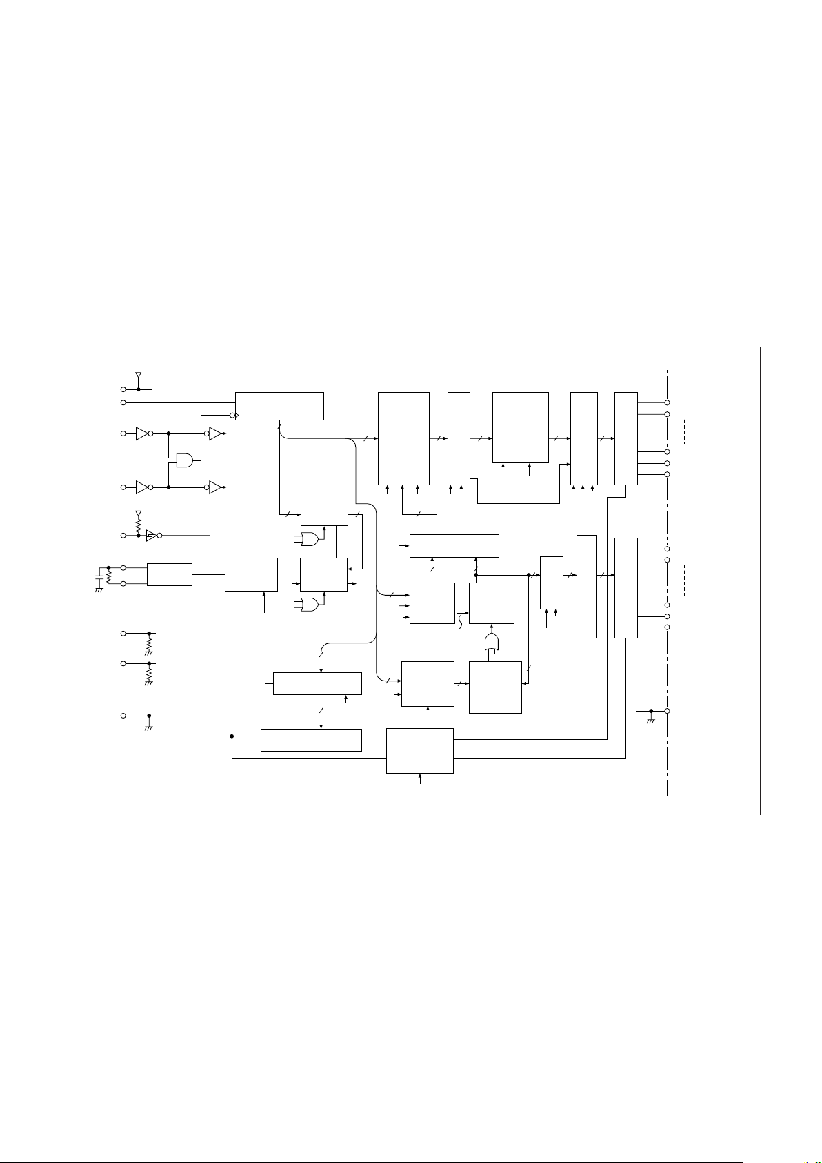
BLOCK DIAGRAM
SEG
DRIVER
LATCHPLALATCHRAM
8-BIT
SHIFT REGISTER
V
DD
CS
CP
RESET
TEST
STEP
TEST
COUNT
V
SS
OSCI
OSCO
CS
CP
RESET
OSC
SEG1
SEG2
SEG34
SEG35
SEG36
COM1
COM2
COM14
COM15
COM16
V
EE
8
8
b0-7
3
5
b4-6
COMMAND
DECODER
RL
TIMING
GENERATOR
CONTROL
RESET
RESET
CS
CP
D.G
LOAD
4
b0-3
4
b0-3
RESET
R
DUTYCYCLE REGISTER
DUTYCYCLE
COUNTER
b0-3
4
D.G
LOAD
RESET
RESET
DUTY AND
BLANK
GENERATOR
RESET
4
DIGIT
COUNT
REGISTER
BA
A = B
ADDRESS
COMP
W.A.C. COUNT
W.A.C. COUNT
W.A.C. LOAD
b0-3
4
WRITE
ADDRESS
COUNTER
READ
ADDRESS
COUNTER
44 4416
W/R
ADDRESS
SELECTOR
4
DISPLAY
DATA
BUFFER
8BITS ¥
16 WORDS
8 7 35 36
fW
RAMPC
LR
ROM
PC1
ROM
PC2
fR
RESET
fDIG
RESET
LATCH
BLANK
DUTY AND BLANK
DECODER
fSEG
RESET
LT
LR S
CHARACTER
GENERATOR
35 ¥ 128 BITS
OE
OE
COM
DRIVER
DA
Page 3
¡ Semiconductor MSC7128-xx
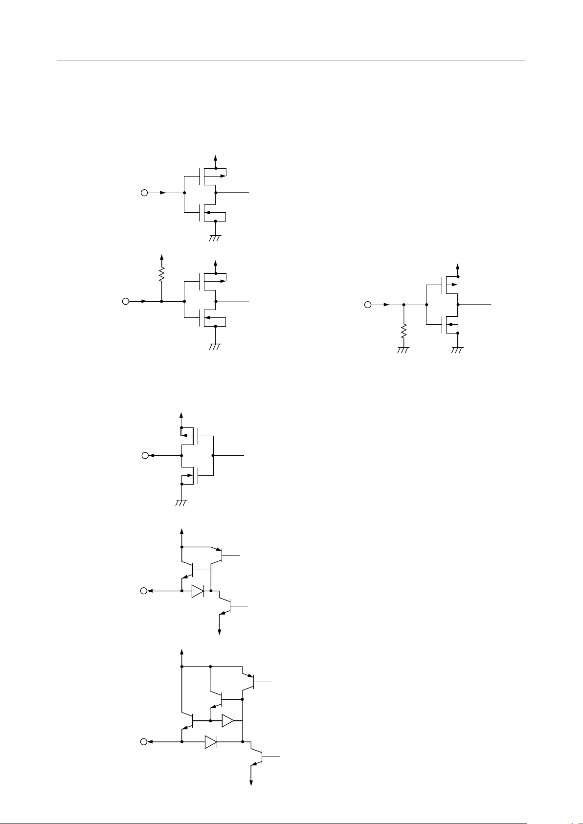
INPUT AND OUTPUT CONFIGURATION
• INPUT PIN
V
DD
DA
CS
CP
OSCI
V
DD
R
V
DD
RESET
• OUTPUT PIN
OSCO
TEST COUNT
TEST STEP
GND
V
DD
V
DD
SEG1 - 35
SEG36
COM1-16
V
V
DD
EE
V
EE
3/27
Page 4
¡ Semiconductor MSC7128-xx
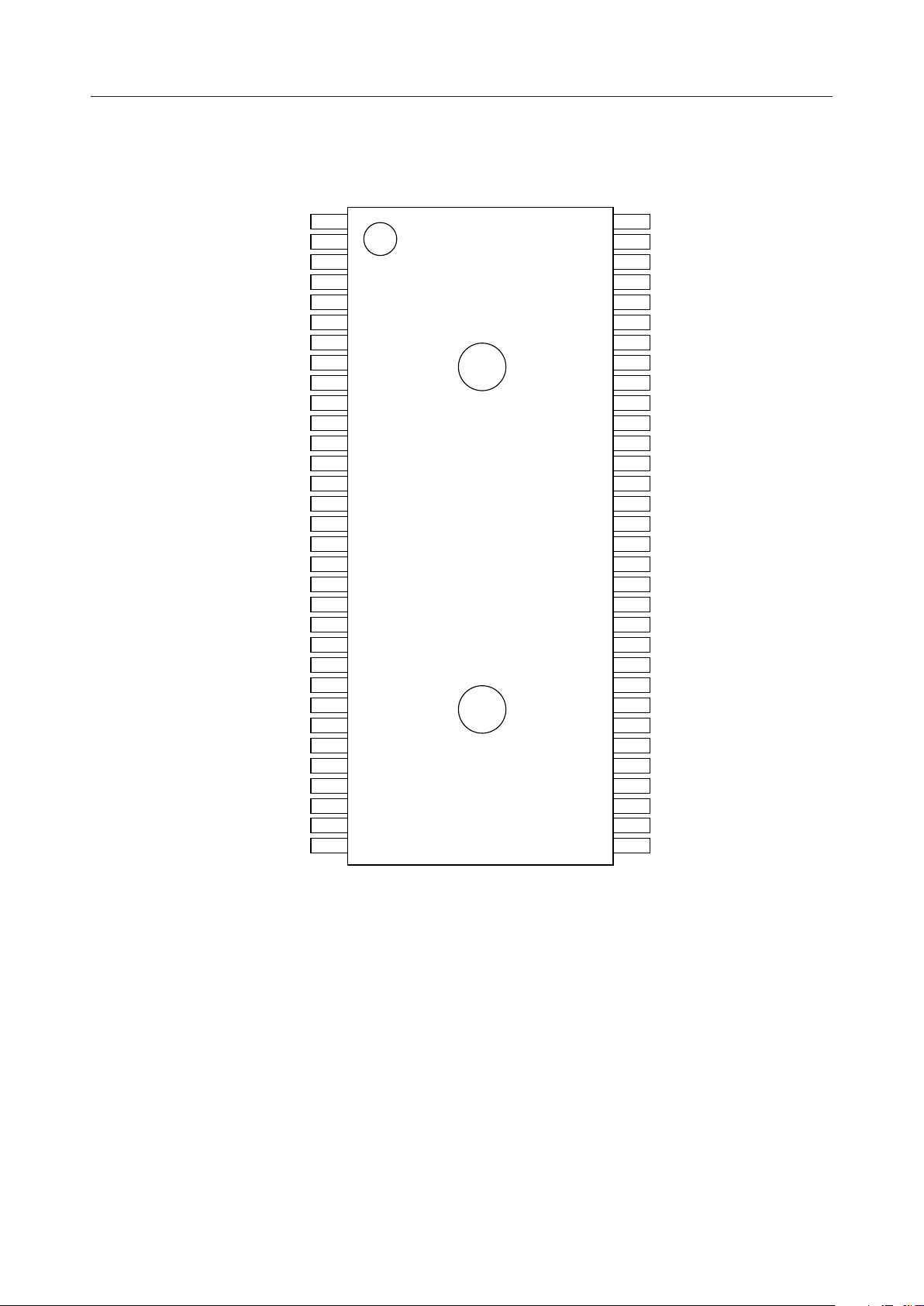
PIN CONFIGURATION (TOP VIEW)
OSC0
OSCI
TEST COUNT
TEST STEP
V
SS
V
EE
COM 1
COM 2
COM 3
COM 4
COM 5
COM 6
COM 7
COM 8
COM 9
COM10
COM11
COM12
COM13
COM14
COM15
COM16
SEG 36
SEG 35
SEG 34
SEG 33
SEG 32
SEG 31
SEG 30
SEG 29
SEG 28
SEG 27
10
11
12
13
14
15
16
17
18
19
20
21
22
23
24
25
26
27
28
29
30
31
32
1
2
3
4
5
6
7
8
9
64
63
62
61
60
59
58
57
56
55
54
53
52
51
50
49
48
47
46
45
44
43
42
41
40
39
38
37
36
35
34
33
CS
DA
CP
RESET
1
V
DD
V
2
DD
SEG 1
SEG 2
SEG 3
SEG 4
SEG 5
SEG 6
SEG 7
SEG 8
SEG 9
SEG 10
SEG 11
SEG 12
SEG 13
SEG 14
SEG 15
SEG 16
SEG 17
SEG 18
SEG 19
SEG 20
SEG 21
SEG 22
SEG 23
SEG 24
SEG 25
SEG 26
64-Pin Plastic Shrink DIP
4/27
Page 5
¡ Semiconductor MSC7128-xx
,
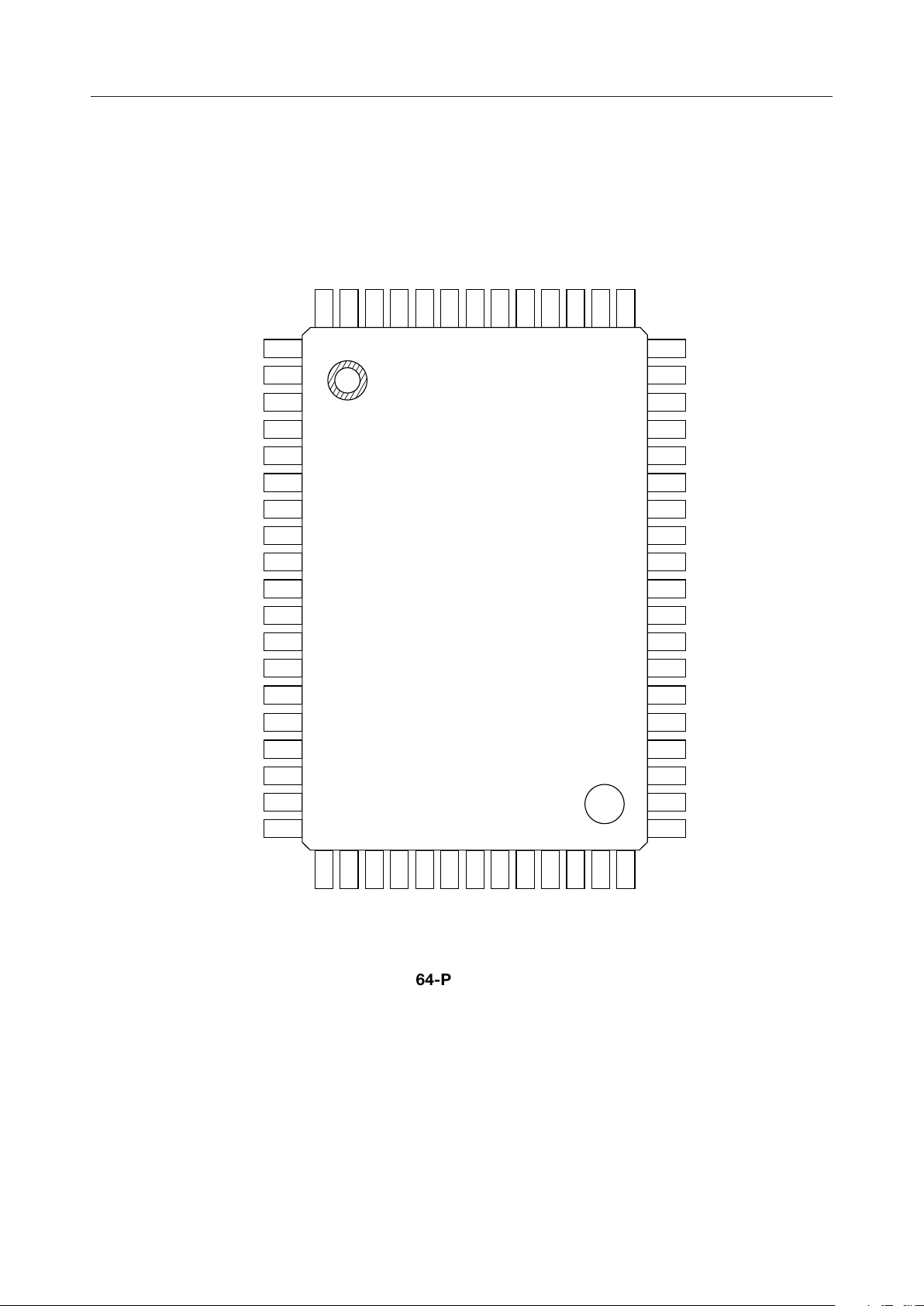
PIN CONFIGURATION (TOP VIEW)
SS
EE
V
COM 1
64
63
V
TEST STEP
62
61
OSC O
OSC I
TEST COUNT
60
59
58
CS
57
DA
56
CP
55
DD1VDD2
RESET
V
54
53
52
COM 2
COM 3
COM 4
COM 5
COM 6
COM 7
COM 8
COM 9
COM 10
COM 11
COM 12
COM 13
COM 14
COM 15
COM 16
SEG 36
SEG 35
SEG 34
SEG 33
3
4
5
6
7
8
9
10
11
12
13
14
15
16
17
18
19
1
2
51
50
49
48
47
46
45
44
43
42
41
40
39
38
37
36
35
34
33
SEG 1
SEG 2
SEG 3
SEG 4
SEG 5
SEG 6
SEG 7
SEG 8
SEG 9
SEG 10
SEG 11
SEG 12
SEG 13
SEG 14
SEG 15
SEG 16
SEG 17
SEG 18
SEG 19
20
SEG 3221SEG 3122SEG 3023SEG 2924SEG 2825SEG 27
26
27
SEG 25
SEG 26
28
29
SEG 24
SEG 23
30
31
SEG 22
SEG 21
32
SEG 20
64-Pin Plastic QFP
5/27
Page 6
¡ Semiconductor MSC7128-xx
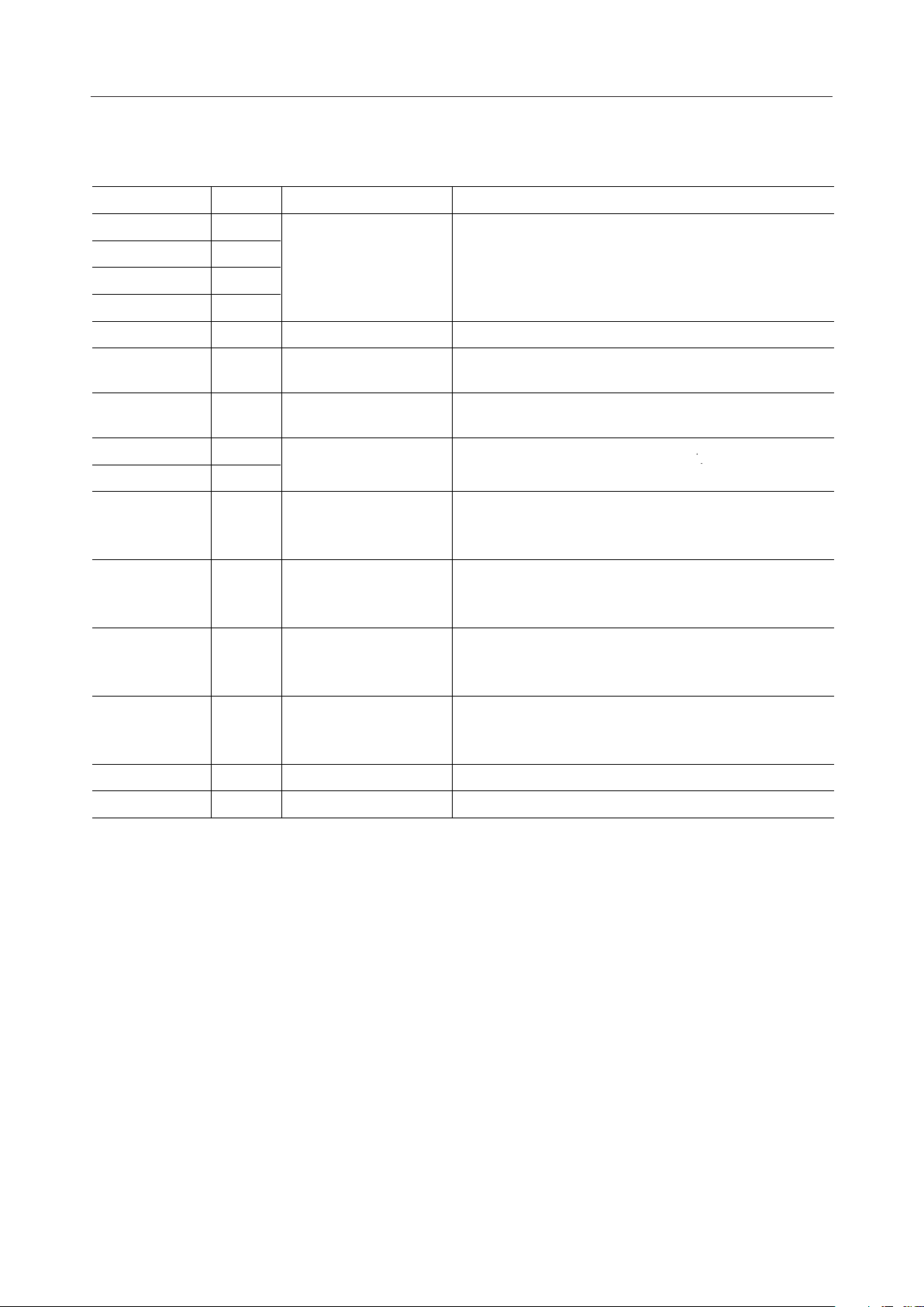
PIN DESCRIPTION
Symbol Type Description
V
V
V
V
DD1
DD2
SS
EE
—
—
—
—
Connected to
Power source
– VSS: Internal logic supply voltage
V
DD1
V
– VEE: VF tube driving circuit supply voltage
DD2
DA I Serial data input from LSB (positive logic)Microcomputer
CP I Microcomputer
CS I Microcomputer
OSCI I
—
OSCO O
Shift clock input. Data is shifted at the leading edge of
the CP.
Chip select input. When the PIN is High, the serial data
transfer is inhibited.
RC oscillation, external RC pin. f
C = 100pF and R = 47kW.
Reset input (pull-up resistor built in). When the pin is
RESET I
—
Low, the internal logic is reset, and the outputs of SEG1
to SEG36 and COM1 to COM16 are Low.
COM1
~
COM16
SEG1
~
SEG35
O VF tube grid electrode
O VF tube anode electrode
VF tube grid electrode driving outputs. This pin can be
connected directly to the VF tube. No pull-down resistor
is required. I
> –30mA
OH
VF tube 5 ¥ 7 -dot anode electrode driving outputs.
This pin can be connected directly to the VF tube. No
pull-down resistor is required. I
VF tube cursor anode electrode driving output.
SEG36 O
VF tube anode electrode
This pin can be connected directly to the VF tube. No
pull-down resistor is required. I
TEST STEP I Test mode setting input (normally open)—
= 250kHz at
OSC
> –2mA
OH
> –10mA
OH
TEST COUNT I Test clock input (normally open)—
6/27
Page 7
¡ Semiconductor MSC7128-xx
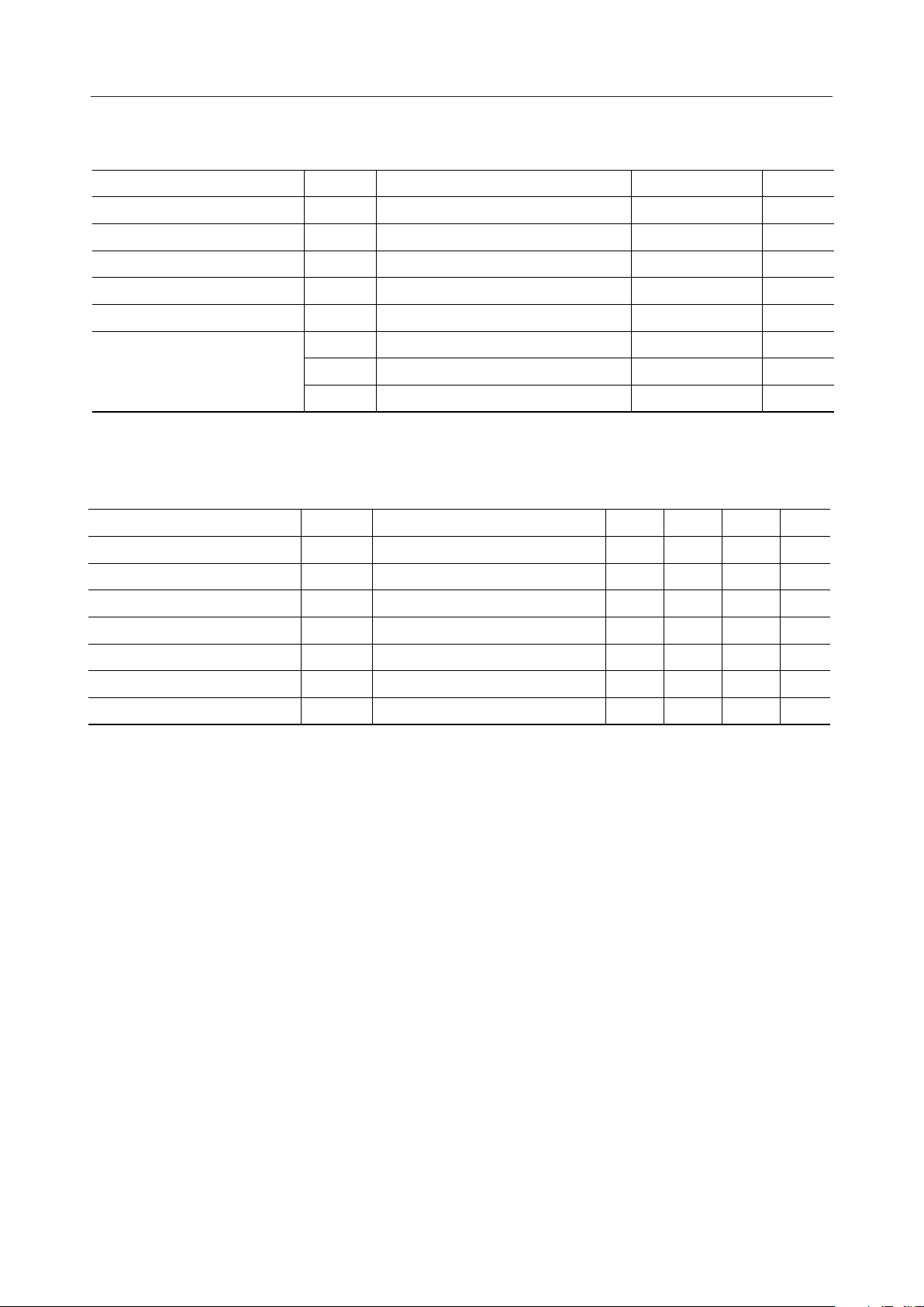
ABSOLUTE MAXIMUM RATINGS
Parameter Symbol Condition Unit
Power Supply Voltage (1) VDD–V
Power Supply Voltage (2) VDD–V
Power Dissipation P
Storage Temperature T
Output Current
STG
I
O1
I
O2
I
O3
SS
EE
SS
D
Ta £ 25°C
COM1 to COM16
SEG1 to SEG35
SEG36
RECOMMENDED OPERATING CONDITIONS
Parameter Symbol Condition Max. Unit
Power Supply Voltage (1) VDD–V
Power Supply Voltage (2) VDD–V
High Level Input Voltage VIH–V
CP Frequency f
OSC Frequency f
Operating Temperature T
CP
OSC
op
SS
EE
SS
SS
—
—
—
—Low Level Input Voltage VIL–V
—
100pF, 47kW
—
—
—
—Input Voltage VIN–V
—
Min.
4.5
10
DD
Rating
–0.3 to +6.5
0 to 65
–0.3 to V
Up to 1.0
Typ.
—
DD
+ 0.3
5.5 V
60 V—
—V—0.7V
0.3V
DD
500 kHz——
270 kHz220170
+75 °C—–20
V
V
V
W
°C–55 to +150
mA–40
mA–4
mA–15
V——
7/27
Page 8
¡ Semiconductor MSC7128-xx
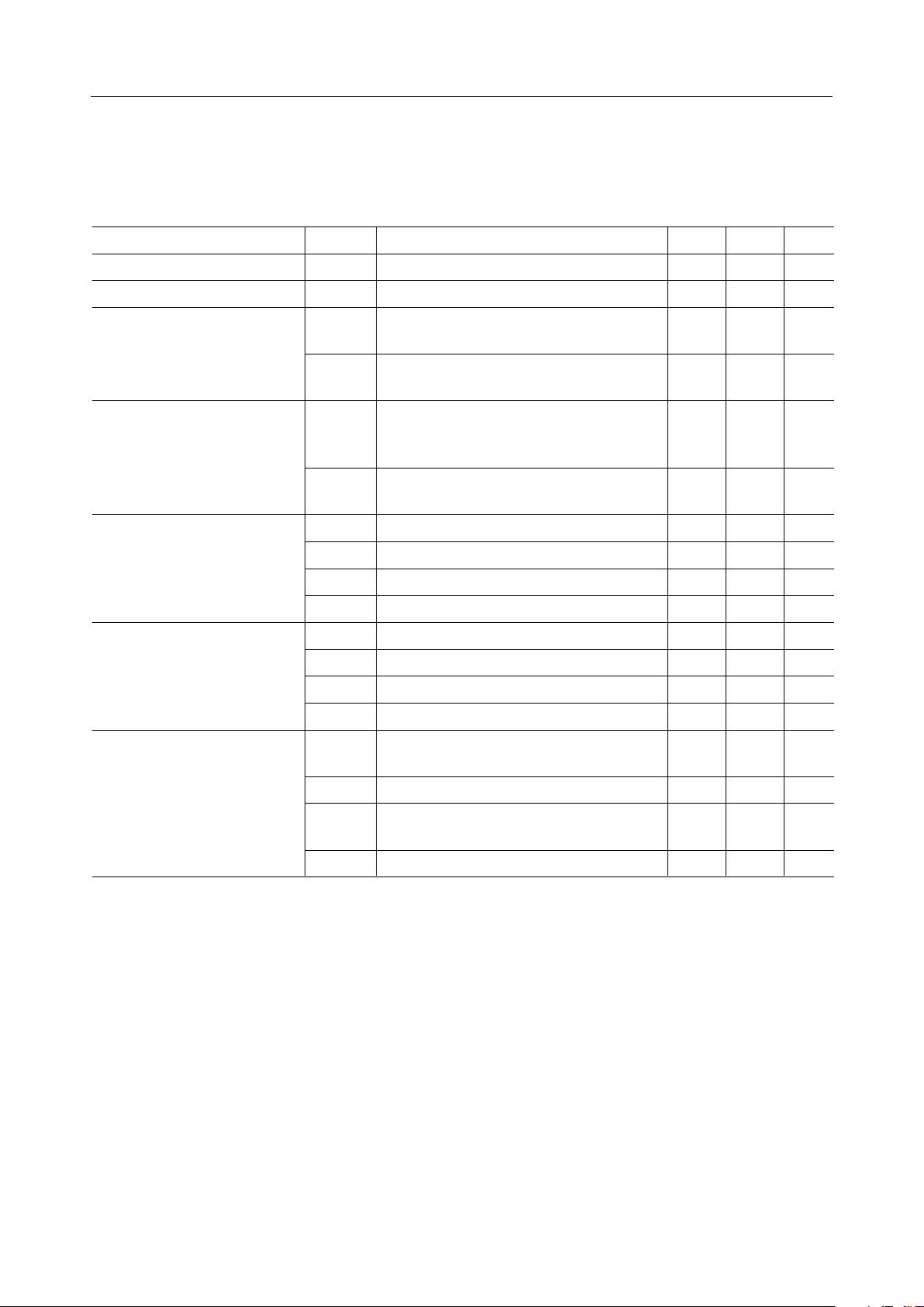
ELECTRICAL CHARACTERISTICS
DC Characteristics
(V
= 5V±10%, VDD–VEE = 60V, Ta = –20 to +75°C)
DD–Vss
Parameter Symbol Condition Max. Unit
High Level Input Voltage V
High Level Input Current
Low Level Input Current
V
V
High Level Output Voltage
V
V
V
V
Low Level Output Voltage
V
V
I
I
I
I
I
IH
IL
IH1
IH2
IL1
IL2
OH1
OH2
OH3
OH4
OL1
OL2
OL3
OL4
SS1
—
—Low Level Input Voltage V
DA, CP, CS
RESET
TEST STEP
TEST COUNT
V
V
V
V
= 5.5V
DD
= 5V
IN
= 5.5V
DD
= 5V
IN
DA, CP, CS
TEST STEP
TEST COUNT
RESET V
OSCO I
COM1~16 I
SEG1~35 I
SEG36 I
OSCO I
COM1~16 I
SEG1~35 I
SEG36 I
V
= 5.5V
DD
V
= 0.5V
IH
= 5.5V
DD
V
= 0.5V
IH
= –500mA
OH
= –30mA
OH
= –2mA
OH
= –10mA
OH
= 500mA
OL
= 100mA
OL
= 100mA
OL
= 100mA
OL
All SEGs on, 16-digit display, duty
cycle 15/16, no load
Min.
0.7V
—V
DD
0.3V
5 mA–5
1mA0.25
5 mA–5
–100 mA–25
—VVDD–0.6
—VVDD–4
—VVDD–3
—VVDD–4
VSS+0.6 V—
VEE+3 V—
VEE+3 V—
VEE+3 V—
15 mA—
DD
V—
Current Consumption
I
I
I
SS2
EE1
EE2
All SEGs Low, all COMs High
All SEGs on, 16-digit display, duty
cycle 15/16, no load
All SEGs Low, all COMs High
1.5 mA—
1.0 mA—
15 mA—
8/27
Page 9
¡ Semiconductor MSC7128-xx
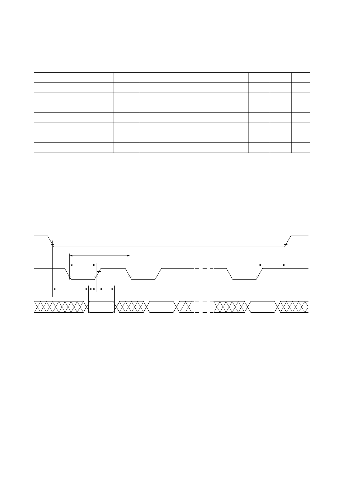
AC Characteristics
Parameter Symbol Condition Max. Unit
CP Cycle Time t
CP Pulse Width t
Data Set-up Time t
Data Hold Time t
CS Set-up Time t
CS Hold Time t
OSC Frequency f
*T = 1/f
OSC
TIMING DIAGRAM
Data Timing
CP
WCP
DS
DH
CSS
CSH
OSC
(V
—
—
—
—
—
—
R = 47kW, C = 100pF
= 5V±10%, Ta = –20 to +75°C)
DD–VSS
Min.
2
— ms
— ms1
— ms0.5
— ms0.5
— ms1
—s32T*
270 kHz170
0.3
t
CSS
t
WCP
t
DS
0.7
0.3
t
CP
0.7
0.3
t
DH
VALID
0.3 0.3
VALID VALID
t
0.3
CSH
9/27
Page 10
¡ Semiconductor MSC7128-xx
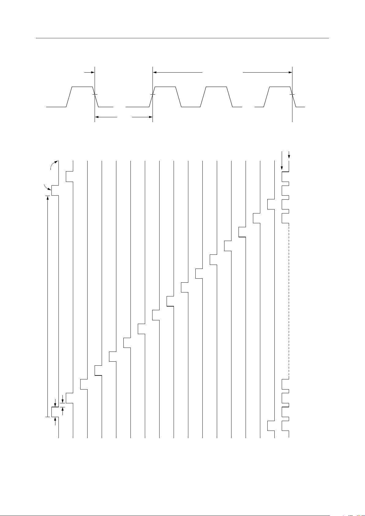
Data LSB/MSB Timing
END OF
DATA WORD
CP
MSB LSB
t
DOFF
DATA INPUT OFF TIME t
Digit Timing (16-Digit Display)
EE
V
DD
V
= 32Tmin (T=1/f
DOFF
OSC
)
NEXT
DATA WORD
DDVEE
V
16=1024T
¥
=64
1
t
2
t
60T
COM 1
3
t
4T
COM 3
COM 2
t1 = Frame count
t
= Display timing
2
t3 = Blank timing
T = 1/f
COM 4
OSC
COM 5
COM 6
COM 7
COM 8
COM 9
COM 10
When
COM 12
COM 11
f
= 245kHz
OSC
t
= 4.096ms
1
t2 = 240ms
t3 = 16ms
COM 13
COM 14
COM 15
SEG n
COM 16
n = 1 to 36
10/27
Page 11
¡ Semiconductor MSC7128-xx
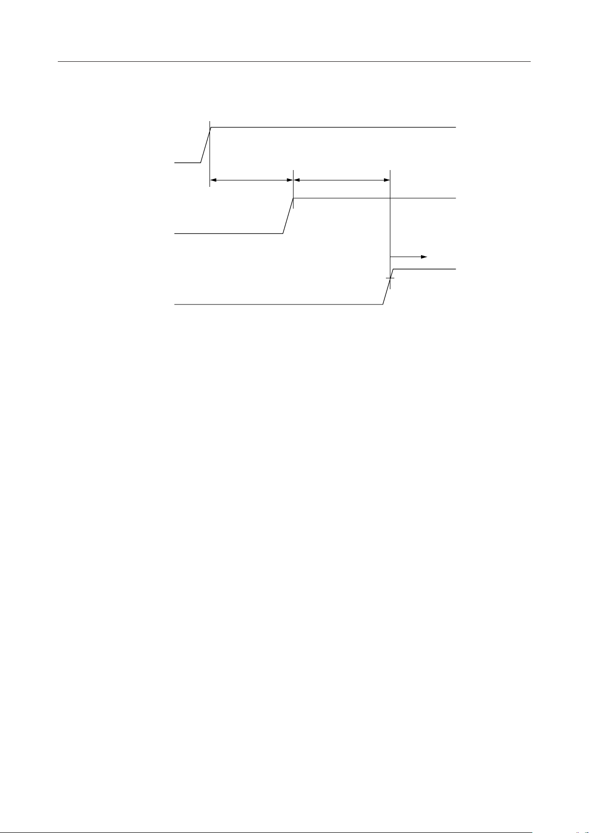
Reset Timing
V
DD
t
RESET OFF
RESET
DA
t
RESET ON
OPTION 1
When a capacitor is connected between the RESET pin and VSS,
RESET ON TIME t
RESET OFF TIME t
ON : 250ms typ.
RESET
OFF : 50ms min.
RESET
(External capacitor : 1mF)
OPTION 2
DATA VALID
When a RESET signal is externally input,
RESET ON TIME t
RESET OFF TIME t
ON : 50ms min.
RESET
OFF : 50ms min.
RESET
11/27
Page 12
¡ Semiconductor MSC7128-xx
FUNCTIONAL DESCRIPTION
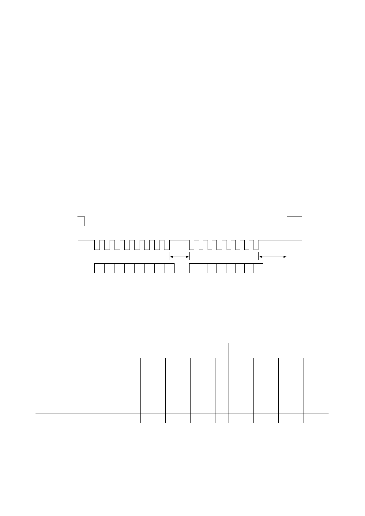
Data Transfer Method and Command Write Method
A display control command or data is written by the 8-bit serial transfer method. The figure
below shows the write timing. When the CS pin is Low, data can be transferred. Data of 8 bits
in length is input to the DA pin sequentially starting with the LSB. (LSB first)
Data is shifted at the rising edge of a shift clock pulse which is input to the CP pin as shown in
the figure below. When 8-bit data is entered, an inner LOAD signal is automatically generated,
and data is written into the registers and RAM. Therefore, there is no need to input an external
LOAD signal.
If the CS pin is changed from Low to High, the serial transfer is inhibited, and data, which is
entered after the CS pin is changed from High to Low, is recognized in units of 8 bits.
The first 8 bits become the first byte, and the second 8 bits become the second byte and the next
8 bits become either the first byte or the second byte depending on the selected command.
CS
CP
DA
*1 t
*2 t
: Refer to Data LSB/MSB Timing.
DOFF
: Refer to AC Characteristics and Data Timing.
CSH
Command Type
No.
Address Set
0
Character Code Set
1
Display Duty Set
2
Number of Display Digits Set
3
Lamp Test
4
Command
*1 t
t
DOFF
b0 b1 b2 b3 b4 b5 b6 b7 b0 b1 b2 b3 b4 b5 b6 b7
LSB LSBMSB MSBFirst Byte Second Byte
First Byte Second Byte
b7
b6
b5
b4
b3
b2
b1
b0
b7
1
0
0
0
X
X
X
X
X
1
0
0
1
X
X
X
X
CU
CH
1
0
1
0
X
X
X
X
X
1
0
1
1
X
X
X
X
X
1
1
0
0
X
X
X
X
X
b6
X
X
X
X
*2
CSH
b5
b4
b3
b2
b1
b0
X
X
X
X
X
CH
DC
DG
X
1
0
CH
1
0
DC
1
0
DG
1
0
X
LT
3
2
CH
CH
CH
6
5
X
X
X
X
X
X
CH
4
3
2
DC
DC
3
2
DG
DG
3
2
X
X
*1 When character codes are to be continuously transferred, addresses are automatically
incremented (internally). Accordingly, neither the Address Set command nor the first byte
of the Character Code Set command are required to set the second and the following character
codes.
*2 X : Don’t care
12/27
Page 13
¡ Semiconductor MSC7128-xx
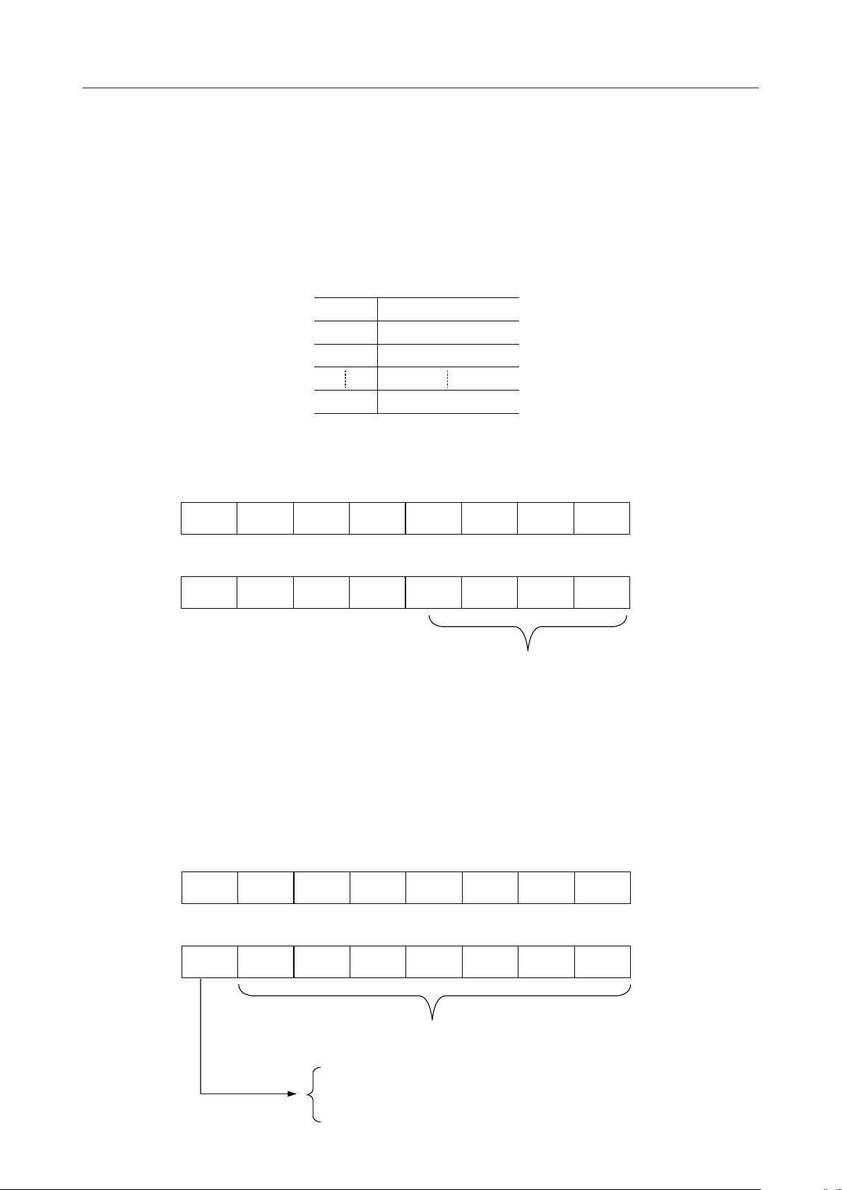
Command Description
• Address set command
When the code of a display character is to be set, this command is used to specify the display
location (digit number) of the character.
The relation between the digit number X and common outputs COM1 to COM16 is as follows:
X COM Input
0 COM1
1 COM2
15 COM16
Command format
LSB
1 000XXXX
1st byte
LSB
XXXX
X
3
X
2
X
1
X
0
2nd byte
Digit number ¥ (0 to 15)
• Character code set command
This command is used to specify the character to be displayed in the digit place specified by the
Address Set command. Bits 0 to 6 of the second byte are used to specify the character code, and
bit 7 is used to specify "Yes" or "No" of cursor display.
Command format
LSB
1
1st byte1 00 XXXX
CU CH
CH
6
CH
5
CH
4
CH
3
CH
2
CH
1
0
2nd byte
7-bit character code
Select one of 128 codes
0: Without cursor (SEG36 OFF)
1: With cursorout (SEG36 ON)
13/27
Page 14
¡ Semiconductor MSC7128-xx
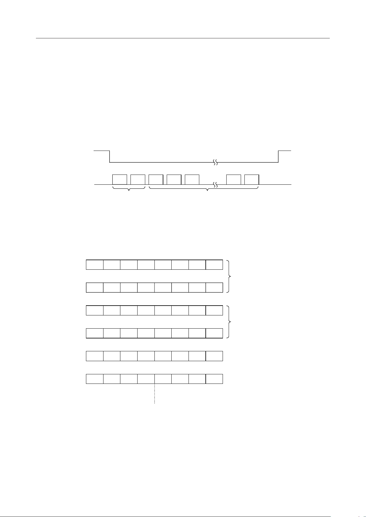
An automatic address increment function is built in. To write multidigit display character codes,
issue the Address Set command. To transfer the second and later digit display character codes,
the first byte (operation code) of the Character Code command is not required. Input the second
byte.
When this command is executed, 8-bit data for the second byte and later bytes, which is provided
before the CS pin is turned High, is all treated as display character data.
Transfer examples of the Address Set command and the Character Set command
CS
DATA
1st 2nd 1st 2nd 2nd 2nd 2nd
Address Set command Character Set command
Example 1: The display for COM3 and the following is changed.
LSB
1000XXXX
LSB
XXXX0 0 1
1001XXXX
CU CH6CH5CH4CH3CH2CH1CH
CU CH6CH5CH4CH3CH2CH1CH
CU CH6CH5CH4CH3CH2CH1CH
0
LSB
LSB
Specify the digit
number X=2
(COM3)
Write the first
character code
0
Write the character
0
code to be displayed
ON COM4
Write the character
0
code to be displayed
ON COM5
X=15 (COM16) is followed by X= 0 (COM1)
14/27
Page 15
¡ Semiconductor MSC7128-xx
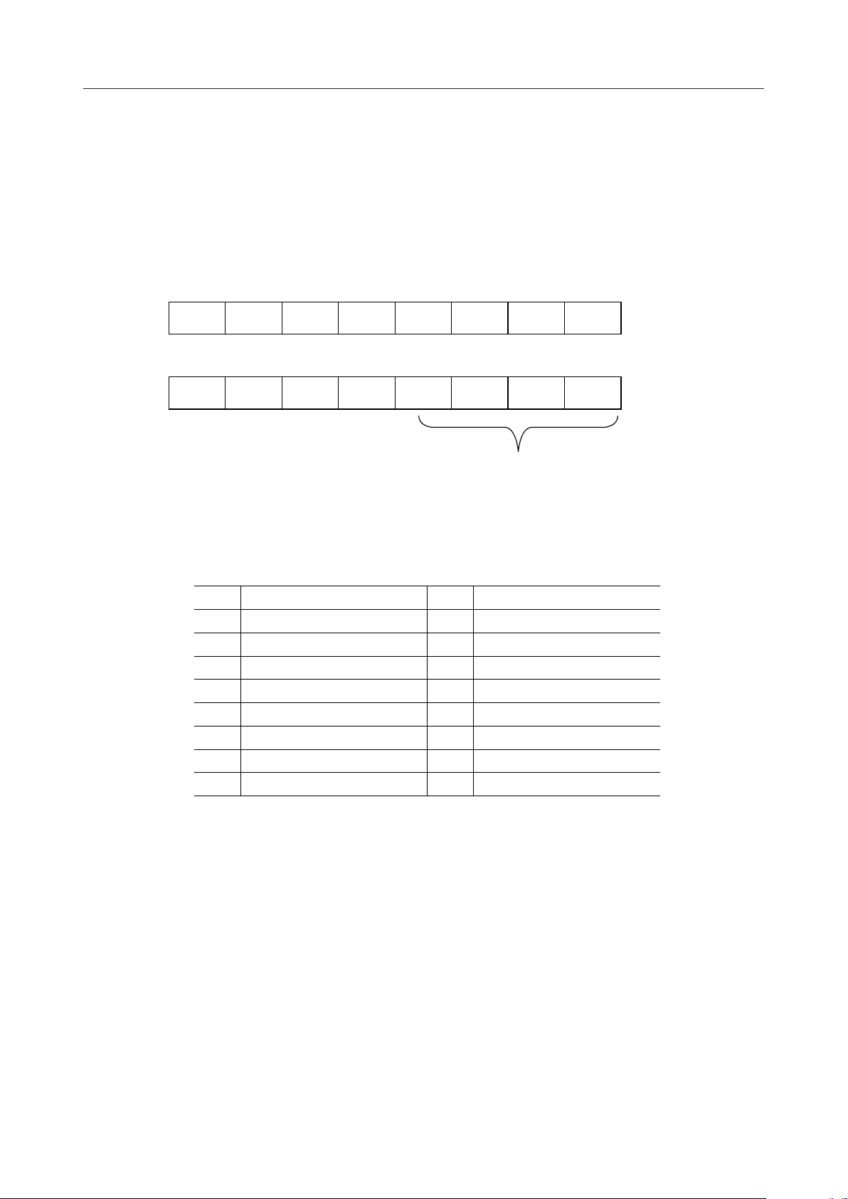
Number of Display Digits Set Command
This command is used to set the digit count register and the number of display digits. The
number of digits to be set ranges from 1 to 16.
Command format
LSB
1 011XXXX
1st byte
LSB
XXXX
DG
DG
3
DG
2
DG
1
0
2nd byte
Number of digits DG (0 to 15)
The relation between the value of DG to be set and COM under display control is as follows:
DG COM Displayed DG COM Displayed
0 COM1 - COM16
1 COM1
2 COM1 - COM2
3 COM1 - COM3
4 COM1 - COM4
5 COM1 - COM5
6 COM1 - COM6
7 COM1 - COM7
8 COM1 - COM8
9 COM1 - COM9
10 COM1 - COM10
11 COM1 - COM11
12 COM1 - COM12
13 COM1 - COM13
14 COM1 - COM14
15 COM1 - COM15
15/27
Page 16
¡ Semiconductor MSC7128-xx
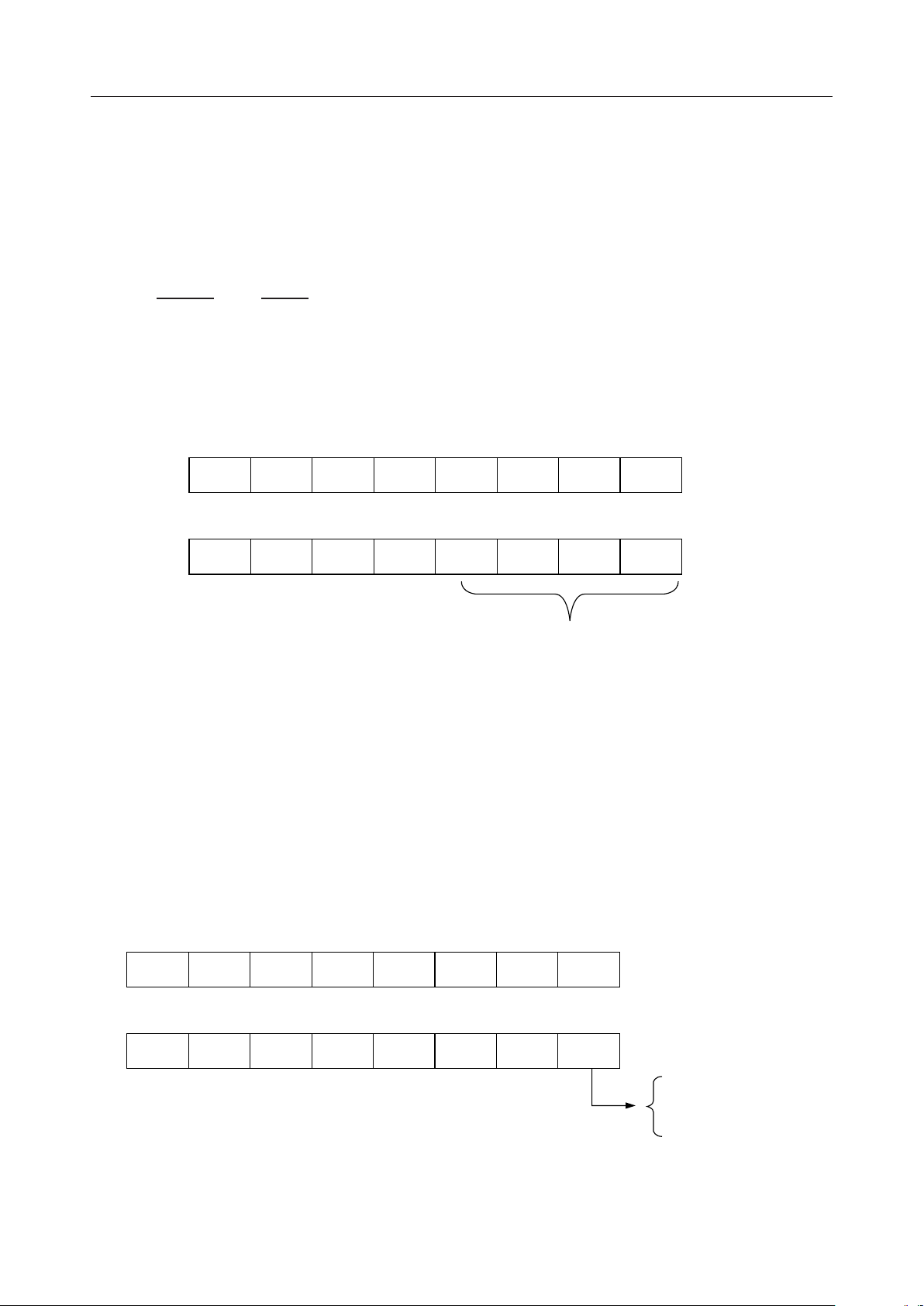
Display Duty Set Command
Assuming the original oscillation cycle as T, the time allocated to 1-digit display is 64T. The actual
display time may be specified as 0 to 60T in increments of 4T. Assuming the number of display
digits as n and the parameter provided by the Display Duty Set command as DC, the resultant
display duty cycle ratio is as follows:
4 (DC)
64n
=
Command format
1 010XXXX
XXXX
Lamp Test Command
(DC)
16n
DG
DG
3
2
DC value (0 to 15)
DG
LSB
1st byte
LSB
DG
1
0
2nd byte
This command is used to set the All-Segment Display mode. If this occurs, the 36 segments for
each digit to be displayed are put into the ON state. The number of display digits and the display
duty cycle depend on the contents of the digit count register and of the duty register.
The contents of the internal RAM are not affected by this command. When the command is
released, the original display appears once again.
Command format
LSB
1100XXXX
LSB
XXXLTXXXX
1st byte
2nd byte
0: Normal mode
1: Lamp test mode
16/27
Page 17

¡ Semiconductor MSC7128-xx
Power On Reset Operation
Operations when the RESET pin is Low are as follows:
a. All segment driver outputs are Low.
b. All grid driver outputs are Low.
c. The number of display digits is set to 16.
d. The display duty cycle is set to 0.
Test Step and Test Count
These pins are used for inspection before shipment, and should not be used by the user.
When this IC is mounted, leave them open or connect to VSS. If they are connected to other pins,
a malfunction may be caused.
17/27
Page 18
¡ Semiconductor MSC7128-xx
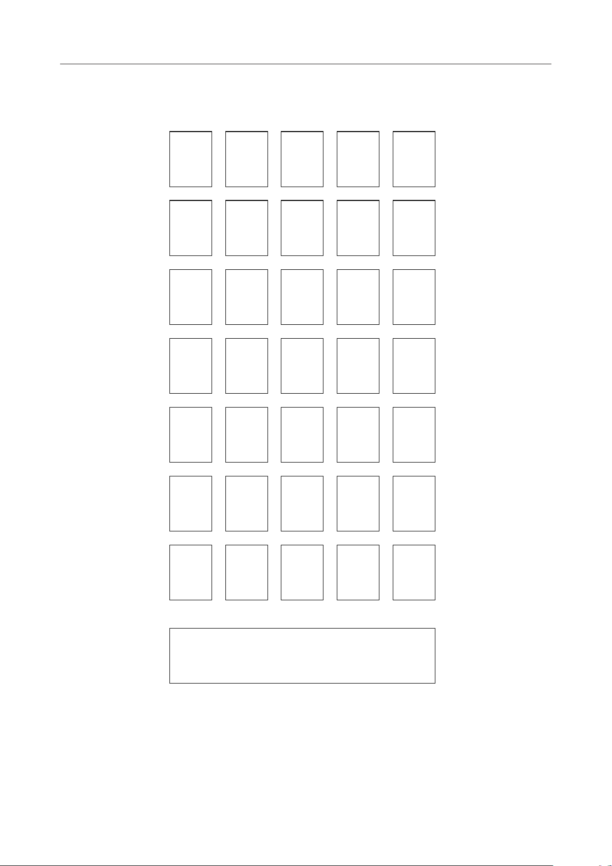
Relation Between Segment Output and VF Tube Dots
1-1
SEG1
1-2
SEG6
1-3
SEG11
1-4
SEG16
1-5
SEG21
2-1
SEG2
2-2
SEG7
2-3
SEG12
2-4
SEG17
2-5
SEG22
3-1
SEG3
3-2
SEG8
3-3
SEG13
3-4
SEG18
3-5
SEG23
4-1
SEG4
4-2
SEG9
4-3
SEG14
4-4
SEG19
4-5
SEG24
5-1
SEG5
5-2
SEG10
5-3
SEG15
5-4
SEG20
5-5
SEG25
1-6
SEG26
1-7
SEG31
2-6
SEG27
2-7
SEG32
3-6
SEG28
3-7
SEG33
Cursor
SEG36
4-6
SEG29
4-7
SEG34
5-6
SEG30
5-7
SEG35
18/27
Page 19
¡ Semiconductor MSC7128-xx
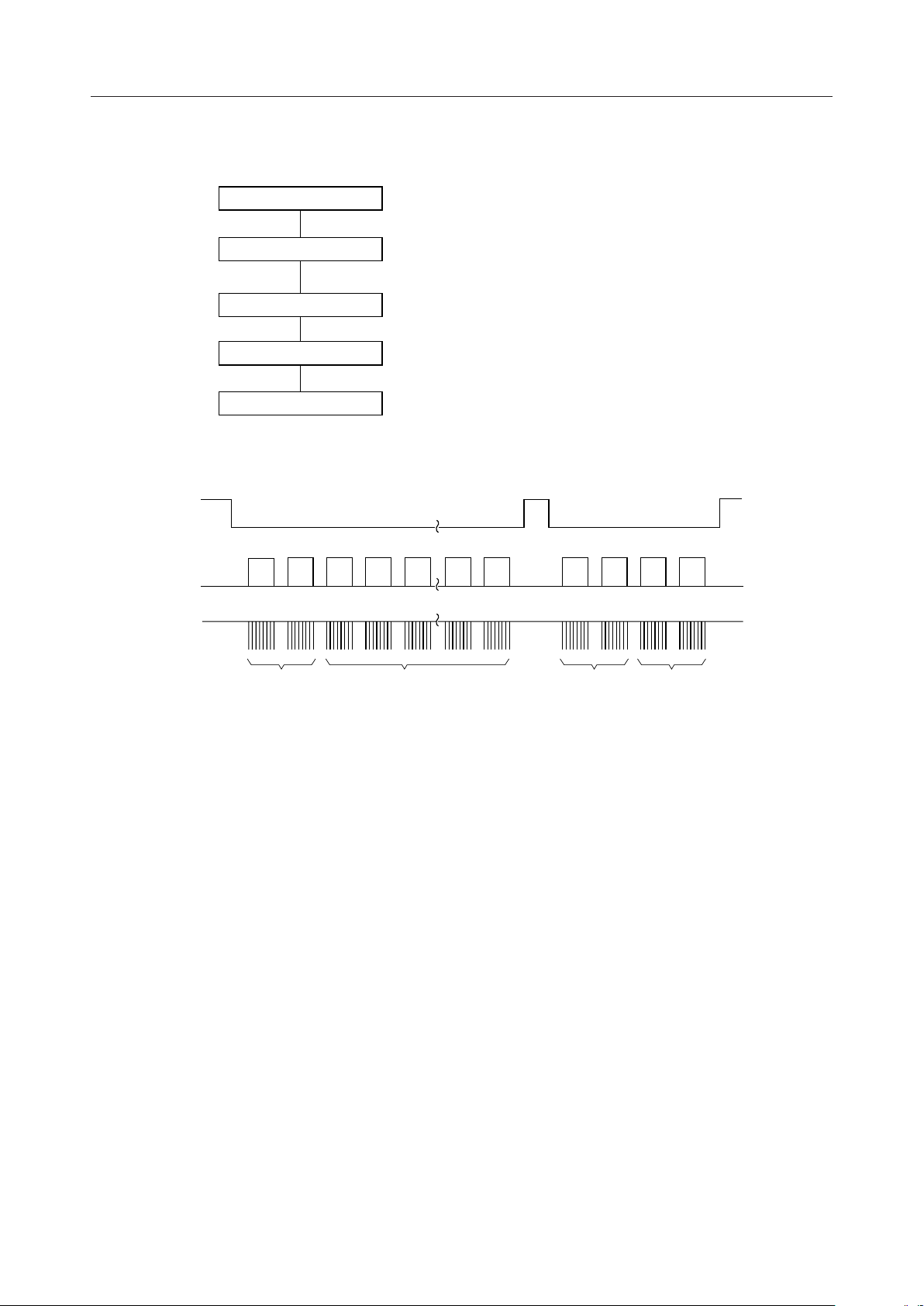
Data Setup Flow
Power on
Address set
Character set
Display digit set
Display duty set
CS
DA
CP
1st 2nd 1st 2nd 2nd 2nd 2nd 1st 2nd 1st 2nd
address set
character set
Number of
display
digits set
Display
duty set
1st : the first byte
2nd : the second byte
Note: To avoid display malfunction due to external noise, re-set occasionally the number of
display digits set and display duty set.
19/27
Page 20
¡ Semiconductor MSC7128-xx
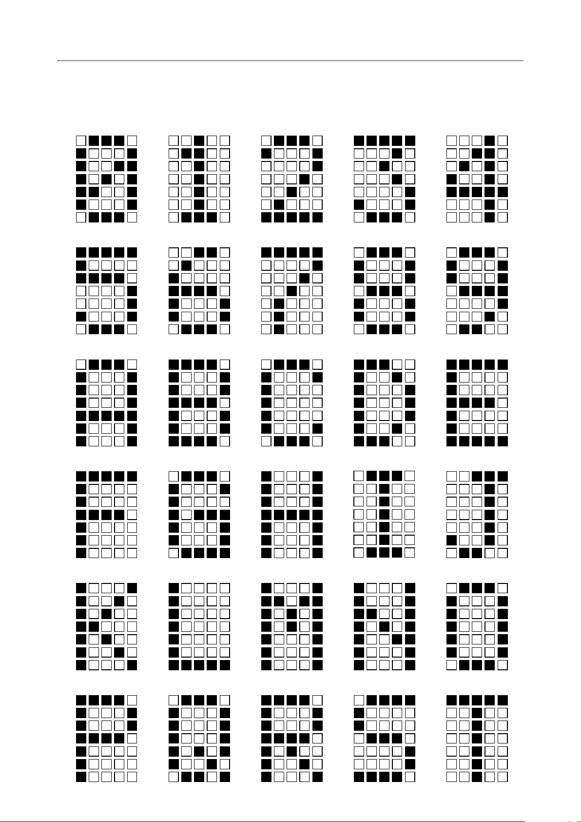
MSC7128-01 ROM CODE
ADDRESS 0(00H) ADDRESS 1(01H) ADDRESS 2(02H) ADDRESS 3(03H) ADDRESS 4(04H)
ADDRESS 5(05H) ADDRESS 6(06H) ADDRESS 7(07H) ADDRESS 8(08H) ADDRESS 9(09H)
ADDRESS 10(0AH) ADDRESS 11(0BH) ADDRESS 12(0CH) ADDRESS 13(0DH) ADDRESS 14(0EH)
ADDRESS 15(0FH) ADDRESS 16(10H) ADDRESS 17(11H) ADDRESS 18(12H) ADDRESS 19(13H)
ADDRESS 20(14H) ADDRESS 21(15H) ADDRESS 22(16H) ADDRESS 23(17H) ADDRESS 24(18H)
ADDRESS 25(19H) ADDRESS 26(1AH) ADDRESS 27(1BH) ADDRESS 28(1CH) ADDRESS 29(1DH)
20/27
Page 21
¡ Semiconductor MSC7128-xx
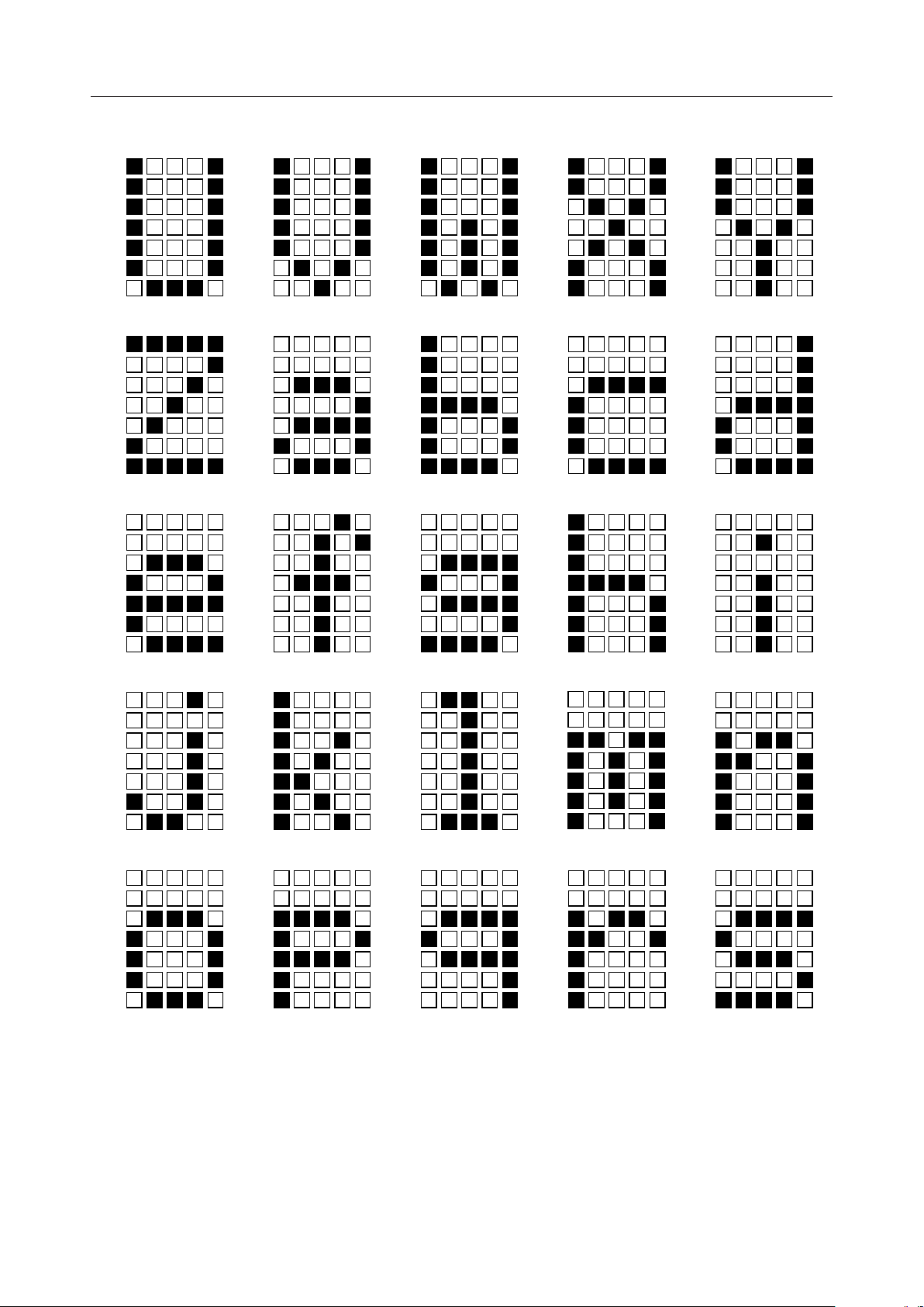
ADDRESS 30(1EH) ADDRESS 31(EFH) ADDRESS 32(20H) ADDRESS 33(21H) ADDRESS 34(22H)
ADDRESS 35(23H) ADDRESS 36(24H) ADDRESS 37(25H) ADDRESS 38(26H) ADDRESS 39(27H)
ADDRESS 40(28H) ADDRESS 41(29H) ADDRESS 42(2AH) ADDRESS 43(2BH) ADDRESS 44(2CH)
ADDRESS 45(2DH) ADDRESS 46(2EH) ADDRESS 47(2FH) ADDRESS 48(30H) ADDRESS 49(31H)
ADDRESS 50(32H) ADDRESS 51(33H) ADDRESS 52(34H) ADDRESS 53(35H) ADDRESS 54(36H)
21/27
Page 22
¡ Semiconductor MSC7128-xx
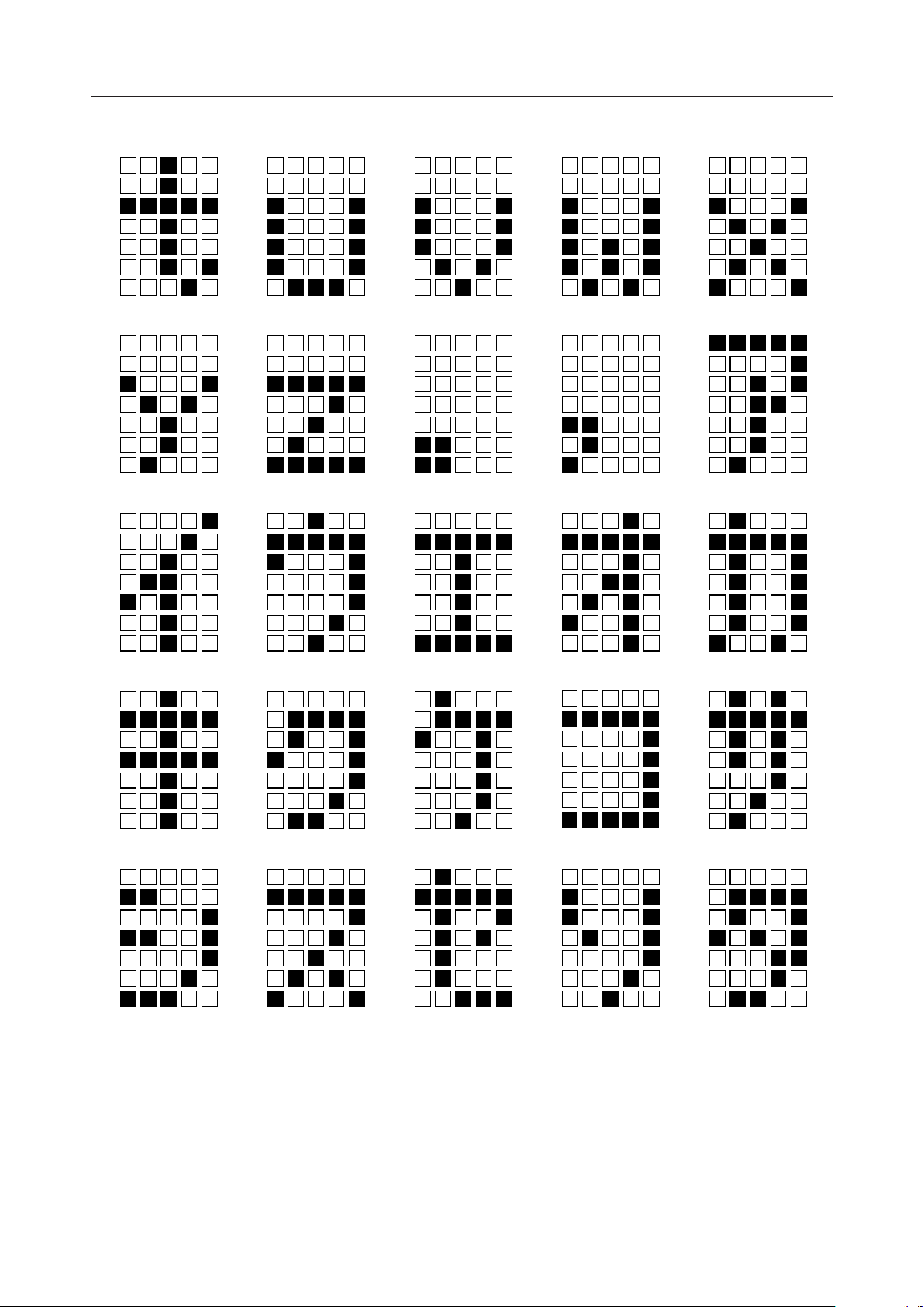
ADDRESS 55(37H) ADDRESS 56(38H) ADDRESS 57(39H) ADDRESS 58(3AH) ADDRESS 59(3BH)
ADDRESS 60(3CH) ADDRESS 61(3DH) ADDRESS 62(3EH) ADDRESS 63(3FH) ADDRESS 64(40H)
ADDRESS 65(41H) ADDRESS 66(42H) ADDRESS 67(43H) ADDRESS 68(44H) ADDRESS 69(45H)
ADDRESS 70(46H) ADDRESS 71(47H) ADDRESS 72(48H) ADDRESS 73(49H) ADDRESS 74(4AH)
ADDRESS 75(4BH) ADDRESS 76(4CH) ADDRESS 77(4DH) ADDRESS 78(4EH) ADDRESS 79(4FH)
22/27
Page 23
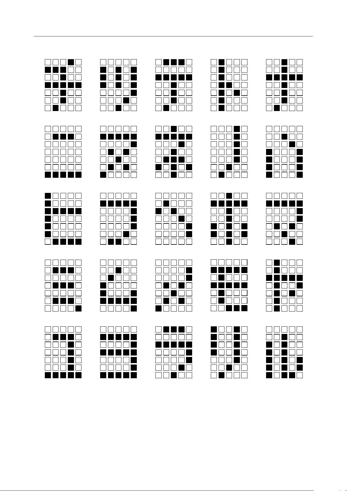
¡ Semiconductor MSC7128-xx
ADDRESS 80(50H) ADDRESS 81(51H) ADDRESS 82(52H) ADDRESS 83(53H) ADDRESS 84(54H)
ADDRESS 85(55H) ADDRESS 86(56H) ADDRESS 87(57H) ADDRESS 88(58H) ADDRESS 89(59H)
ADDRESS 90(5AH) ADDRESS 91(5BH) ADDRESS 92(5CH) ADDRESS 93(5DH) ADDRESS 94(5EH)
ADDRESS 95(5FH) ADDRESS 96(60H) ADDRESS 97(61H) ADDRESS 98(62H) ADDRESS 99(63H)
ADDRESS 100(64H) ADDRESS 101(65H) ADDRESS 102(66H) ADDRESS 103(67H) ADDRESS 104(68H)
23/27
Page 24
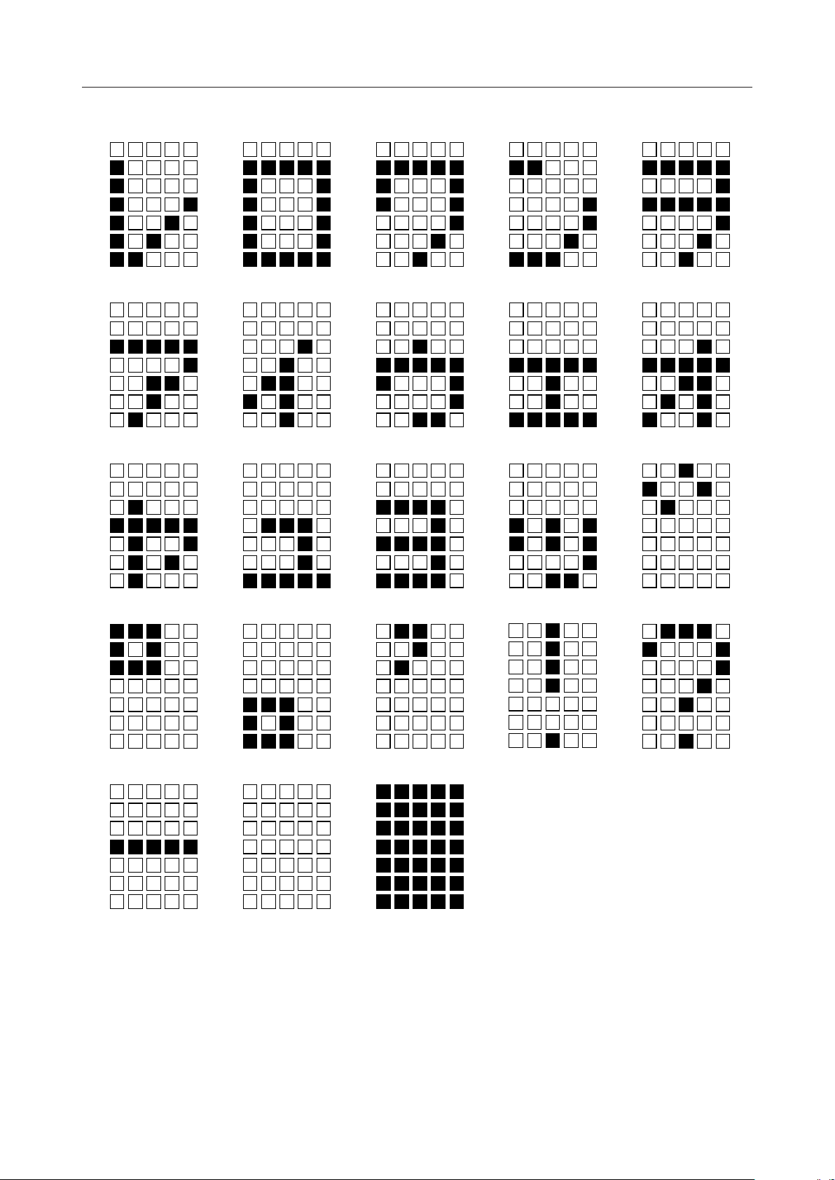
¡ Semiconductor MSC7128-xx
ADDRESS 105(69H) ADDRESS 106(6AH) ADDRESS 107(6BH) ADDRESS 108(6CH) ADDRESS 109(6DH)
ADDRESS 110(6EH) ADDRESS 111(6FH) ADDRESS 112(70H) ADDRESS 113(71H) ADDRESS 114(72H)
ADDRESS 115(73H) ADDRESS 116(74H) ADDRESS 117(75H) ADDRESS 118(76H) ADDRESS 119(77H)
ADDRESS 120(78H) ADDRESS 121(79H) ADDRESS 122(7AH) ADDRESS 123(7BH) ADDRESS 124(7CH)
ADDRESS 125(7DH) ADDRESS 126(7EH) ADDRESS 127(7FH)
24/27
Page 25
¡ Semiconductor MSC7128-xx
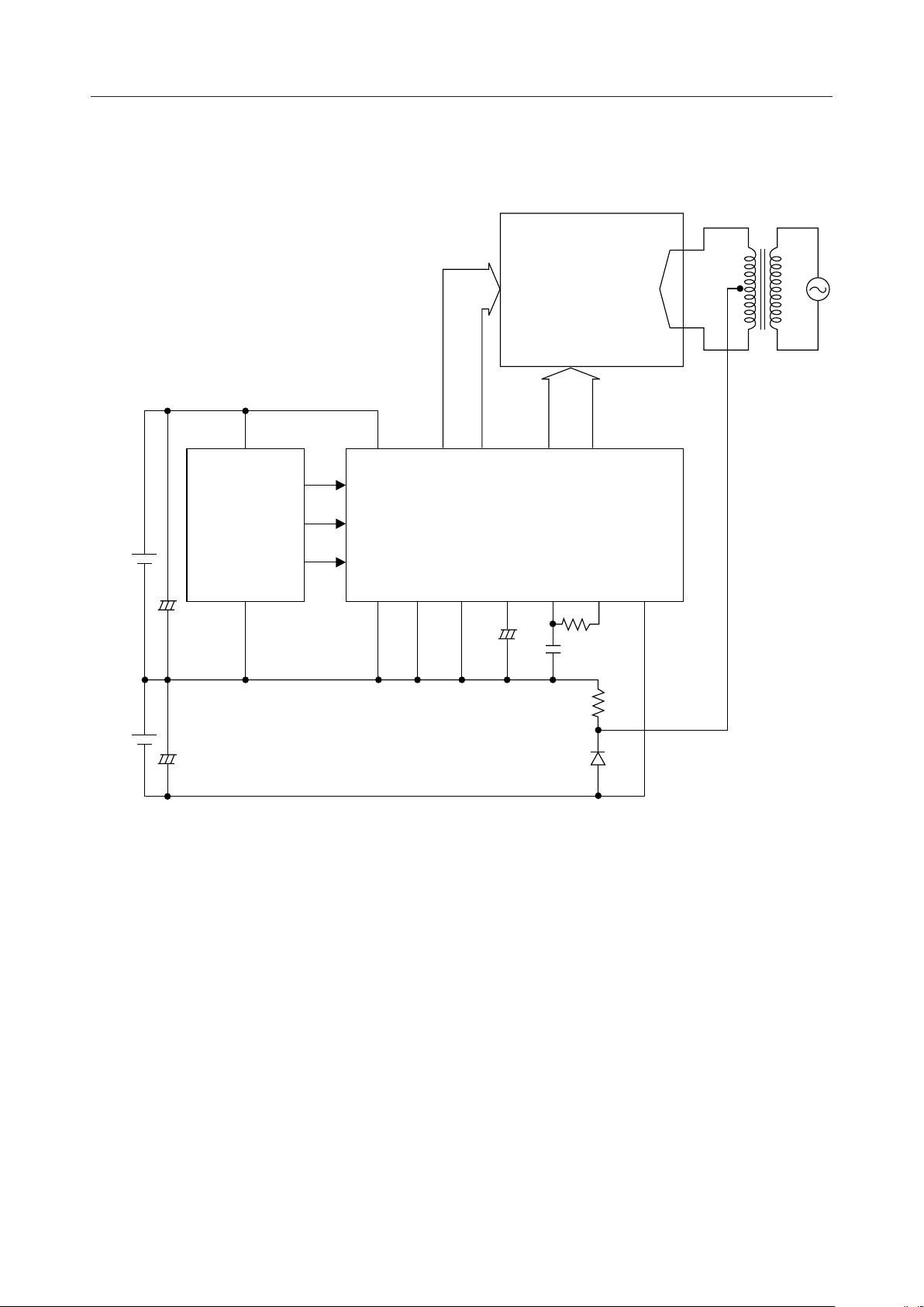
APPLICATION CIRCUIT
Heater Transformer
VF Display
ANODE
(SEGMENT)
GRID (DIGIT)
+5V
+60V
V
DD
DD
SEG1 - 36 COM1 - 16V
DA
MCU
Output
Port
CP
MSC7128-xx
CS
TEST
+
GND
V
SS
–
STEP
TEST
COUNT
RESET
+
–
OSCI OSCO V
R
C
EE
R1
+
–
ZD
25/27
Page 26
¡ Semiconductor MSC7128-xx
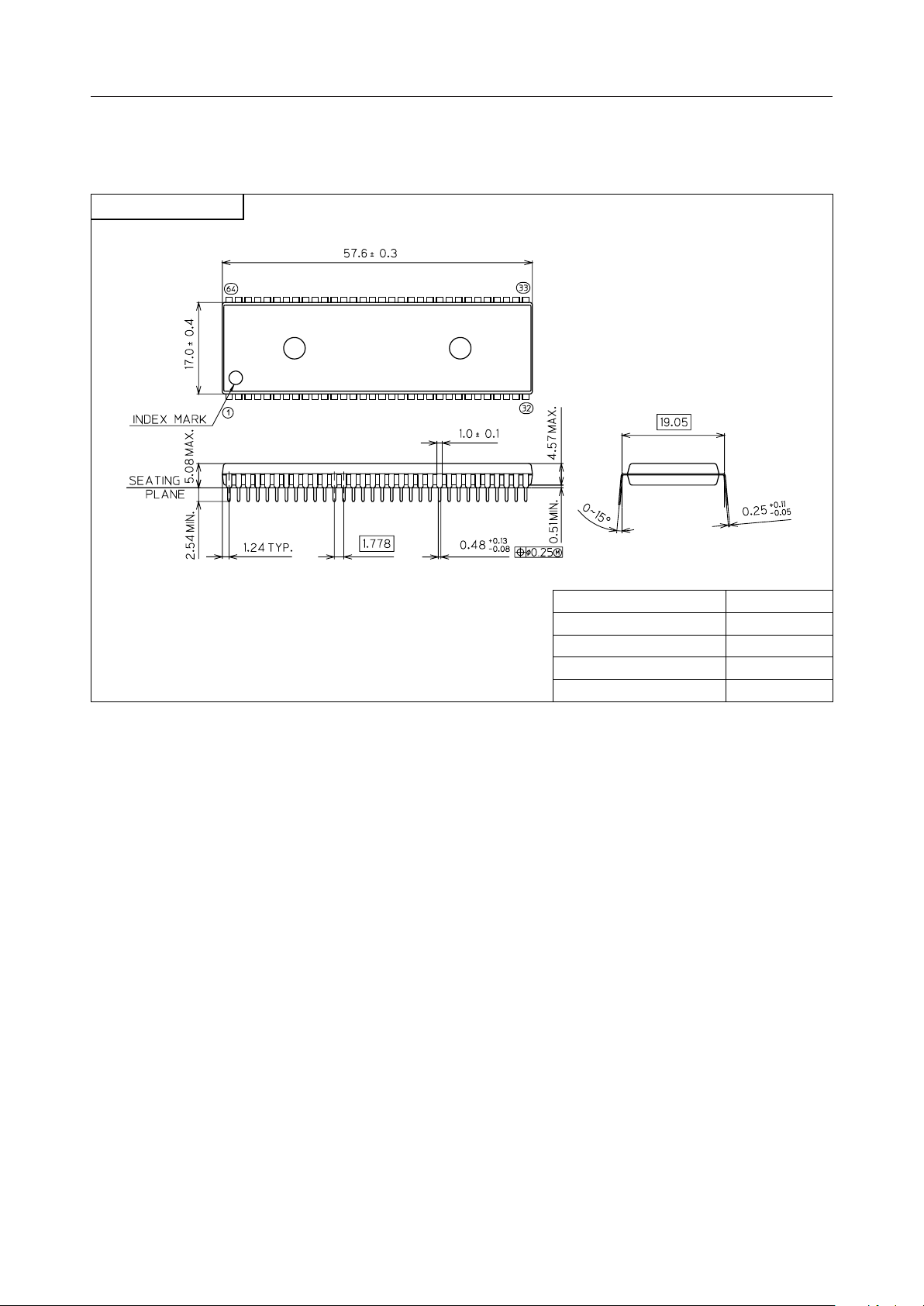
PACKAGE DIMENSIONS
(Unit : mm)
SDIP64-P-750-1.78
Package material
Lead frame material
Pin treatment
Solder plate thickness
Package weight (g)
Epoxy resin
Cu alloy
Solder plating
5 mm or more
8.70 TYP.
Notes for Mounting the Surface Mount Type Package
The SOP, QFP, TSOP, SOJ, QFJ (PLCC), SHP and BGA are surface mount type packages, which
are very susceptible to heat in reflow mounting and humidity absorbed in storage.
Therefore, before you perform reflow mounting, contact Oki’s responsible sales person for the
product name, package name, pin number, package code and desired mounting conditions
(reflow method, temperature and times).
26/27
Page 27
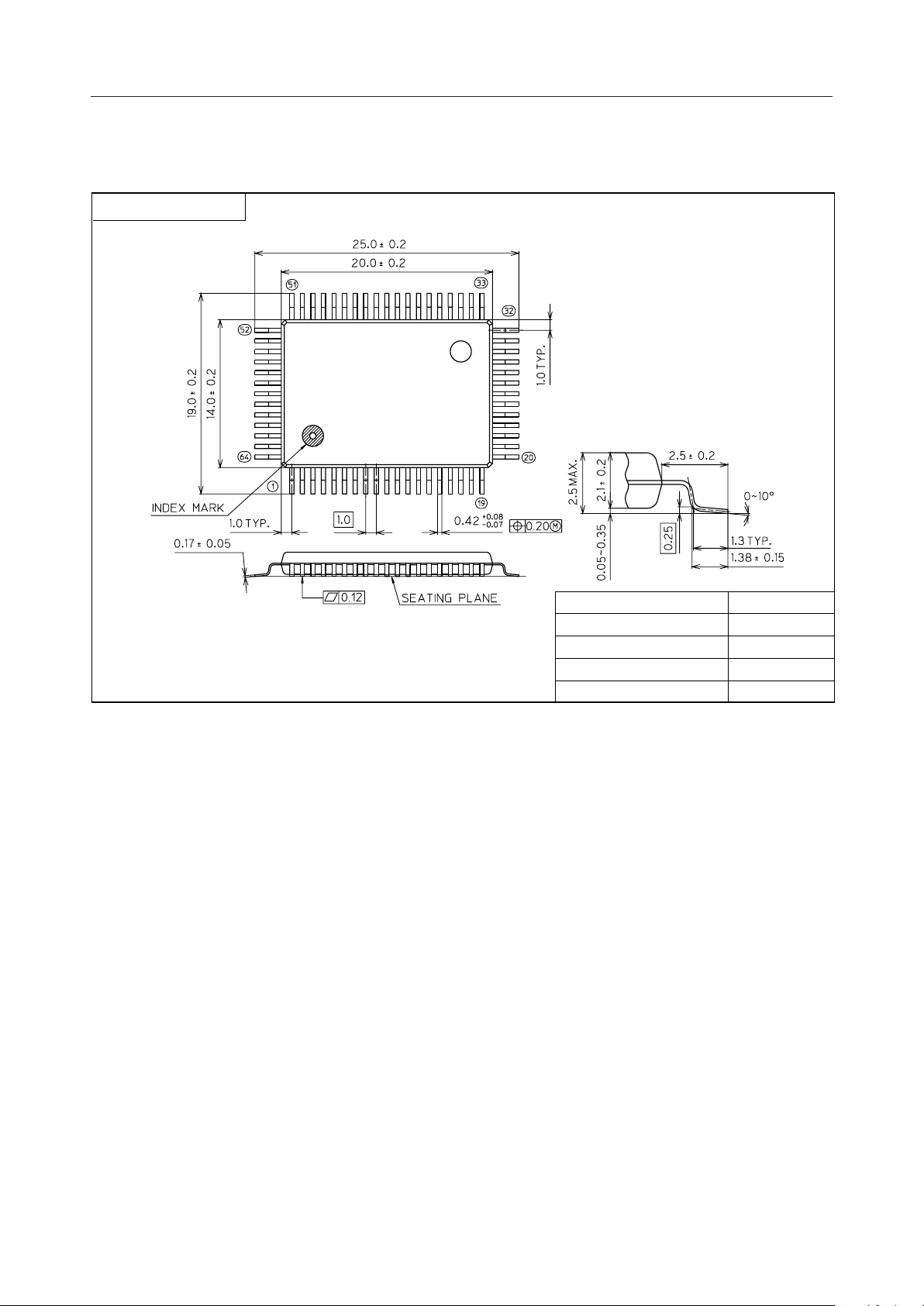
¡ Semiconductor MSC7128-xx
(Unit : mm)
QFP64-P-1420-1.00-BK
Mirror finish
Package material
Lead frame material
Pin treatment
Solder plate thickness
Package weight (g)
Epoxy resin
42 alloy
Solder plating
5 mm or more
1.25 TYP.
Notes for Mounting the Surface Mount Type Package
The SOP, QFP, TSOP, SOJ, QFJ (PLCC), SHP and BGA are surface mount type packages, which
are very susceptible to heat in reflow mounting and humidity absorbed in storage.
Therefore, before you perform reflow mounting, contact Oki’s responsible sales person for the
product name, package name, pin number, package code and desired mounting conditions
(reflow method, temperature and times).
27/27
 Loading...