

Datasheet MSC23837A-70BS18, MSC23837A-60BS18, MSC23837A-70DS18, MSC23837A-60DS18 Datasheet (OKI)
Page 1
MSC23837A-xxBS18/DS18¡ Semiconductor
¡ Semiconductor
MSC23837A-xxBS18/DS18
8,388,608-Word ¥ 36-Bit DRAM MODULE : FAST PAGE MODE TYPE
DESCRIPTION
The Oki MSC23837A-xxBS18/DS18 is a fully decoded 8,388,608-word ¥ 36-bit CMOS dynamic
random access memory composed of eighteen 16-Mb DRAMs (4M ¥ 4) in SOJ packages mounted
with decoupling capacitors on a 72-pin glass epoxy SIMM Package. This module is generally
used for memory expansion in parity applications such as workstations.
FEATURES
• 8,388,608-word ¥ 36-bit (ECC) organization
• 72-pin SIMM
MSC23837A-xxBS18 : Gold tab
MSC23837A-xxDS18 : Solder tab
• Single 5 V supply ±10% tolerance
• Input : TTL compatible
• Output : TTL compatible, 3-state
• Refresh : 4096 cycles/64 ms
• CAS before RAS refresh, CAS before RAS hidden refresh, RAS-only refresh capability
• Multi-bit test mode capability
• Fast Page Mode capability
PRODUCT FAMILY
Family
MSC23837A-60BS18/DS18
MSC23837A-70BS18/DS18
Access Time (Max.)
RACtAAtCAC
60 ns
30 ns
15 ns
70 ns
35 ns
20 ns
t
OEA
15 ns
20 ns
Cycle Time
(Min.)
110 ns
130 ns
Power Dissipation
Operating (Max.)
5197.5 mW
4702.5 mW
Standby (Max.)t
99 mW
215
Page 2
MSC23837A-xxBS18/DS18 ¡ Semiconductor
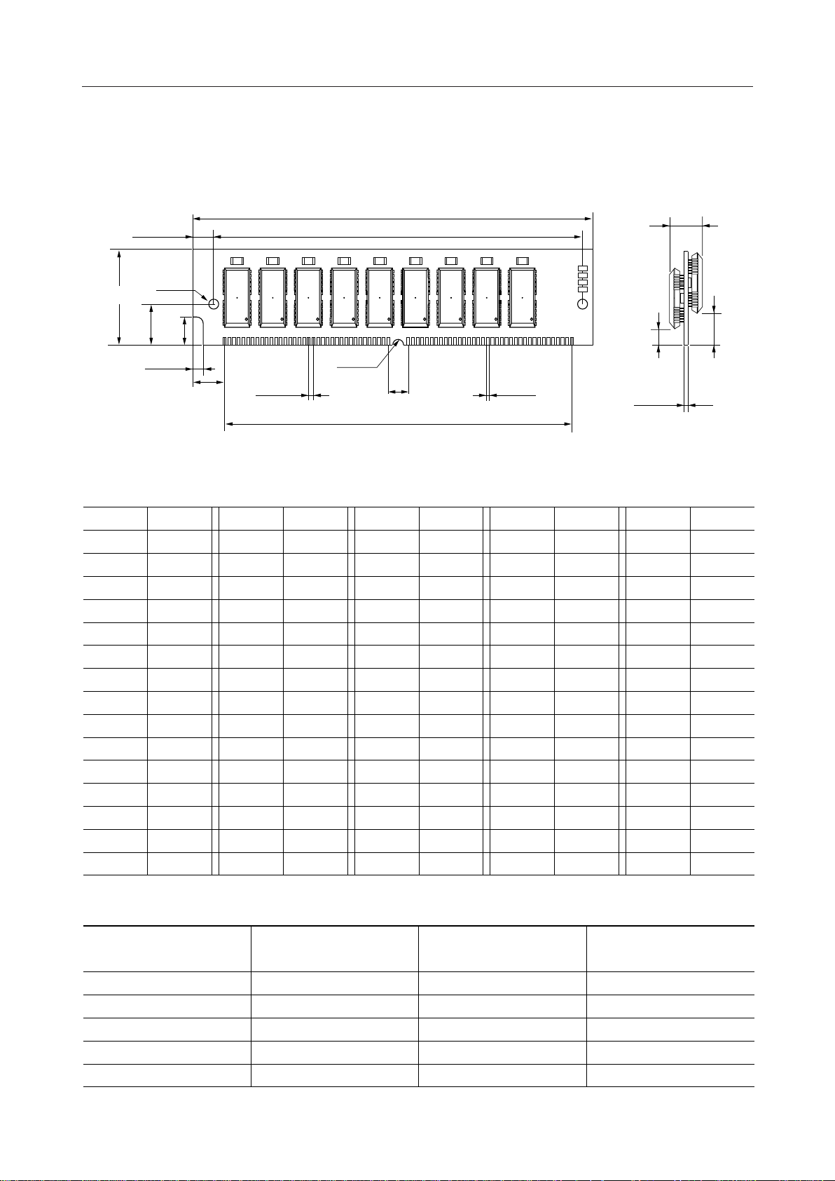
PIN CONFIGURATION
MSC23837A-xxBS18/DS18
3.18φ
25.4 ±0.2
Typ.
Typ.
10.16
2.03 Typ.
6.35
6.35 Typ.
1
1.27 ±0.1
*1 The common size difference of the board width 12.5 mm of its height is
specified as ±0.2. The value above 12.5 mm is specified as ±0.5.
107.95 ±0.2
101.19 Typ.3.38 ±0.2
R1.57
6.35
95.25
*1
1.04 Typ.
72
3.5 Min.
1.27
(Unit : mm)
9.3 Max.
6.5 Min.
+0.1
–0.08
Pin No.
Pin Name
11631
2 173247
3 183348
4 193449
5 203550
6 213651
7 223752
8 233853
9 243954
10 25 40 55
11 26 41 56
12 27 42 57
13 28 43 58
14 29 44 59
15 30 45 60
V
SS
DQ0 A5 A9 WE
DQ1 A6 NC NC
DQ2 OE NC DQ22
DQ3 DQ8 DQ17 DQ23
DQ4 DQ9 DQ18 DQ24
DQ5 DQ10 DQ19 DQ25
DQ6 DQ11 DQ20 DQ26
DQ7 DQ12 V
V
CC
PD5 DQ14 A10 DQ29
A0 DQ15 A11 DQ30
A1 A7 CAS1 DQ31
A2 DQ16 RAS0 V
A3 V
Pin No.
Pin Name
A4 A8 DQ21
Pin No.
Pin Name
SS
Pin No.
46
Pin Name
DQ13 CAS0 DQ28
CC
RAS1 DQ32
DQ27
Presence Detect Pins
CC
Pin No.
61
62
63
64
65
66
67
68
69
70
71
72
Pin Name
DQ33
DQ34
DQ35
NC
NC
NC
PD1
PD2
PD3
PD4
NC
V
SS
216
Pin No.
67 PD1
68 PD2
11 PD5
Pin Name
MSC23837A
-60BS18/DS18
NC
V
SS
NC69 PD3
V
SS
MSC23837A
-70BS18/DS18
NC
V
SS
V
SS
NCNC70 PD4
V
SS
Page 3
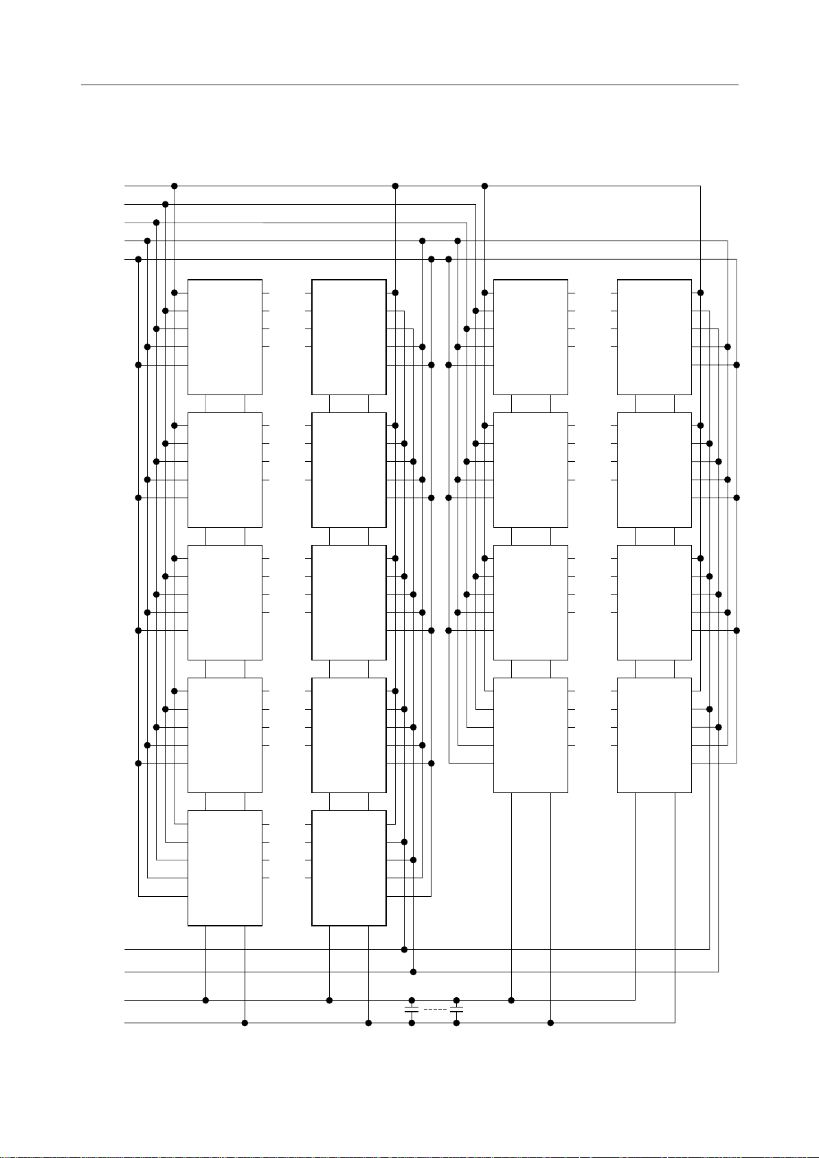
BLOCK DIAGRAM
A0 - A11
RAS0
CAS0
WE
OE
MSC23837A-xxBS18/DS18¡ Semiconductor
A0 - A11
RAS
CAS
WE
OE
V
CC
A0 - A11
RAS
CAS
WE
OE
V
CC
A0 - A11
RAS
CAS
WE
OE
V
CC
A0 - A11
RAS
CAS
WE
OE
V
CC
V
V
V
V
DQ
DQ
DQ
DQ
SS
DQ
DQ
DQ
DQ
SS
DQ
DQ
DQ
DQ
SS
DQ
DQ
DQ
DQ
SS
DQ0
DQ1
DQ2
DQ3
DQ4
DQ5
DQ6
DQ7
DQ8
DQ9
DQ10
DQ11
DQ12
DQ13
DQ14
DQ15
DQ
DQ
DQ
DQ
V
DQ
DQ
DQ
DQ
V
DQ
DQ
DQ
DQ
V
DQ
DQ
DQ
DQ
V
CC
CC
CC
CC
A0 - A11
RAS
CAS
WE
OE
V
SS
A0 - A11
RAS
CAS
WE
OE
V
SS
A0 - A11
RAS
CAS
WE
OE
V
SS
A0 - A11
RAS
CAS
WE
OE
V
SS
A0 - A11
RAS
CAS
WE
OE
V
CC
A0 - A11
RAS
CAS
WE
OE
V
CC
A0 - A11
RAS
CAS
WE
OE
V
CC
A0 - A11
RAS
CAS
WE
OE
V
CC
V
V
V
V
DQ
DQ
DQ
DQ
SS
DQ
DQ
DQ
DQ
SS
DQ
DQ
DQ
DQ
SS
DQ
DQ
DQ
DQ
SS
DQ20
DQ21
DQ22
DQ23
DQ24
DQ25
DQ26
DQ27
DQ28
DQ29
DQ30
DQ31
DQ32
DQ33
DQ34
DQ35
DQ
DQ
DQ
DQ
V
DQ
DQ
DQ
DQ
V
DQ
DQ
DQ
DQ
V
DQ
DQ
DQ
DQ
V
CC
CC
CC
CC
A0 - A11
RAS
CAS
WE
OE
V
SS
A0 - A11
RAS
CAS
WE
OE
V
SS
A0 - A11
RAS
CAS
WE
OE
V
SS
A0 - A11
RAS
CAS
WE
OE
V
SS
RAS1
CAS1
V
V
V
DQ
DQ
DQ
DQ
SS
DQ16
DQ17
DQ18
DQ19
DQ
DQ
DQ
DQ
V
CC
A0 - A11
RAS
CAS
WE
OE
V
SS
C1 C18
A0 - A11
RAS
CAS
WE
OE
V
CC
CC
SS
217
Page 4

MSC23837A-xxBS18/DS18 ¡ Semiconductor
ELECTRICAL CHARACTERISTICS
Absolute Maximum Ratings
Parameter
Voltage on Any Pin Relative to V
Voltage VCC Supply Relative to V
SS
SS
Symbol
V
IN
V
Short Circuit Output Current I
Power Dissipation P
Operating Temperature T
Storage Temperature T
, V
OS
opr
OUT
CC
D
stg
Rating Unit
–1.0 to 7.0 V
–1.0 to 7.0 V
50 mA
18 W
0 to 70 °C
–40 to 125 °C
Note: Permanent device damage may occur if ABSOLUTE MAXIMUM RATINGS are
exceeded. Functional operation should be restricted to the conditions as detailed in the
operational sections of this data sheet. Exposure to absolute maximum rating conditions
for extended periods may affect device reliability.
Recommended Operating Conditions
(Ta = 0°C to 70°C)
Parameter
Power Supply Voltage
Input High Voltage
Input Low Voltage
Symbol
V
CC
V
SS
V
IH
V
IL
Min.
Typ.
4.5 5.0 5.5 V
000V
2.4 — 6.5 V
–1.0 — 0.8 V
Max.
Unit
Capacitance
Parameter
Input Capacitance
(RAS0, RAS1, CAS0, CAS1)
Symbol
C
IN1
C
IN2
C
IN3
C
DQ
Typ.
Note : Capacitance measured with Boonton Meter.
(Ta = 25°C, f = 1 MHz)
Max.
— 122
—73
Unit
pFInput Capacitance (A0 - A11)
pF
pFInput Capacitance (WE, OE) — 140
pFI/O Capacitance (DQ0 - DQ35) — 26
218
Page 5

MSC23837A-xxBS18/DS18¡ Semiconductor
DC Characteristics
Parameter
Input Leakage Current
Output Leakage Current
Output High Voltage
Output Low Voltage
Average Power
Supply Current
(Operating)
Power Supply
Current (Standby)
Average Power
Supply Current
(RAS-only Refresh)
Average Power
Supply Current
(CAS before RAS Refresh)
Average Power
Supply Current
(Fast Page Mode)
Symbol
I
LI
I
LO
V
OH
V
OL
I
CC1
I
CC2
I
CC3
I
CC6
I
CC7
Condition
0 V £ VI £ 6.5 V;
All other pins not
under test = 0 V
disable
D
OUT
0 V £ V
I
OH
I
OL
£ 5.5 V
O
= –5.0 mA
= 4.2 mA
RAS, CAS cycling,
= Min.
t
RC
RAS, CAS = V
IH
RAS, CAS
≥ V
–0.2 V
CC
RAS cycling,
= Min.
,
IH
CAS = V
t
RC
RAS cycling,
CAS before RAS,
= Min.
t
RC
RAS = V
,
IL
CAS cycling,
= Min.
t
PC
(VCC = 5 V ±10%, Ta = 0°C to 70°C)
MSC23837A MSC23837A
-60BS18/DS18 -70BS18/DS18
Min.
–180
–20
2.4
0
—
—
—
—
—
—
Max.
180
20
V
CC
0.4
945
36
18
945
945
855
Min.
–180
–20
2.4
0
—
—
—
—
—
—
Max.
180
20
V
CC
0.4
855
36
18
855
855
765
Unit
µA
µA
V
V
mA
mA
mA
mA
mA
mA
Note
1, 2
1
1
1, 2
1, 2
1, 3
Notes: 1. ICC Max. is specified as ICC for output open condition.
2. Address can be changed once or less while RAS=VIL.
3. Address can be changed once or less while CAS=VIH.
219
Page 6

MSC23837A-xxBS18/DS18 ¡ Semiconductor
AC Characteristics (1/2)
Parameter
Random Read or Write Cycle Time
Read Modify Write Cycle Time t
Fast Page Mode Cycle Time t
Fast Page Mode Read Modify Write Cycle Time
Access Time from RAS t
Access Time from CAS t
Access Time from Column Address t
Access Time from CAS Precharge t
Access Time from OE t
Output Low Impedance Time from CAS
Output Buffer Turn-off Delay Time t
OE to Data Output Buffer Turn-off Delay Time
Transition Time t
Refresh Period t
RAS Precharge Time t
RAS Pulse Width t
RAS Pulse Width (Fast Page Mode) t
RAS Hold Time t
RAS Hold Time referenced to OE t
CAS Precharge Time t
CAS Pulse Width t
CAS Hold Time t
CAS to RAS Precharge Time t
RAS to CAS Delay Time t
RAS to Column Address Delay Time t
Row Address Set-up Time t
Row Address Hold Time t
Column Address Set-up Time t
Column Address Hold Time t
Column Address Hold Time from RAS t
Column Address to RAS Lead Time t
Symbol
t
t
RC
RWC
PC
PRWC
RAC
CAC
AA
CPA
OEA
t
CLZ
OFF
t
OEZ
T
REF
RP
RAS
RASP
RSH
ROH
CP
CAS
CSH
CRP
RHCP
RCD
RAD
ASR
RAH
ASC
CAH
AR
RAL
= 5 V ±10%, Ta = 0°C to 70°C) Note 1,2,3,11,12
(V
CC
MSC23837A
-60BS18/DS18
Min.
110
155
40
85
—
—
—
—
—
0
0
0
3
—
40
60
60
15
10
10
15
60
10
35
20
15
0
10
0
15
50
30
Max.
—
—
—
—
60
15
30
35
15
—
15
15
50
64
—
10k
100k
—
—
—
10k
—
—
—
45
30
—
—
—
—
—
—
MSC23837A
-70BS18/DS18
Min.
130
185
45
100
—
—
—
—
—
0
0
0
3
—
50
70
70
20
10
10
20
70
10
40 ns
20
15
0
10
0
15
55
35
Max.
—
—
—
—
70
20
35
40
20
—
20
20
50
64
—
10k
100k
—
—
—
10k
—
—
—RAS Hold Time from CAS Precharge t
50
35
—
—
—
—
—
—
Unit
ns
ns
ns
ns
ns
ns
ns
ns
ns
ns
ns
ns
ns
ms
ns
ns
ns
ns
ns
ns
ns
ns
ns
ns
ns
ns
ns
ns
ns
ns
ns
Note
4, 5, 6
4, 5
4, 6
4
4
4
7
7
3
5
6
220
Page 7

MSC23837A-xxBS18/DS18¡ Semiconductor
AC Characteristics (2/2)
Parameter
Read Command Set-up Time
Read Command Hold Time t
Read Command Hold Time referenced to RAS
Write Command Set-up Time t
Write Command Hold Time t
Write Command Hold Time from RAS t
Write Command Pulse Width t
OE Command Hold Time t
Write Command to RAS Lead Time t
Write Command to CAS Lead Time t
Data-in Set-up Time t
Data-in Hold Time t
Data-in Hold Time from RAS t
OE to Data-in Delay Time t
CAS to WE Delay Time t
Column Address to WE Delay Time t
RAS to WE Delay Time t
CAS Precharge to WE Delay Time t
CAS Active Delay Time from RAS Precharge
RAS to CAS Set-up Time (CAS before RAS)t
RAS to CAS Hold Time (CAS before RAS)t
WE to RAS Precharge Time (CAS before RAS)
WE Hold Time from RAS (CAS before RAS)t
RAS to WE Set-up Time (Test Mode) t
RAS to WE Hold Time (Test Mode) t
Symbol
t
RCS
RCH
t
RRH
WCS
WCH
WCR
WP
OEH
RWL
CWL
DS
DH
DHR
OED
CWD
AWD
RWD
CPWD
t
RPC
CSR
CHR
t
WRP
WRH
WTS
WTH
(VCC = 5 V ±10%, Ta = 0°C to 70°C) Note 1,2,3,11,12
MSC23837A MSC23837A
-60BS18/DS18 -70BS18/DS18
Min.
0
0
0
0
10
45
10
15
15
15
0
15
50
15
40
55
85
60
10
10
20
10
10
10
20
Max.
—
—
—
—
—
—
—
—
—
—
—
—
—
—
—
—
—
—
—
—
—
—
—
—
—
Min.
0
0
0
0
15
55
10
20
20
20
0
15
55
20
50
65
100
70 ns
10
10
20
10
10
10
20
Max.
—
—
—
—
—
—
—
—
—
—
—
—
—
—
—
—
—
—
—
—
—
—
—
—
—
Unit
ns
ns
ns
ns
ns
ns
ns
ns
ns
ns
ns
ns
ns
ns
ns
ns
ns
ns
ns
ns
ns
ns
ns
ns
Note
8
8
9
10
10
9
9
9
9
221
Page 8

MSC23837A-xxBS18/DS18 ¡ Semiconductor
Notes: 1. A start-up delay of 200 µs is required after power-up followed by a minimum of
eight initialization cycles (RAS-only refresh or CAS before RAS refresh) before
proper device operation is achieved.
When using the internal refresh counter, a minimum of eight CAS before RAS
initialization cycles is required.
2. AC mesurement assume tT = 5 ns.
3. VIH (Min.) and VIL (Max.) are reference levels for measuring input timing signals.
Transition times are measured between VIH and VIL.
4. Measured with a load circuit equivalent to 2 TTL loads and 100 pF.
5. Operation within the t
(Max.) is specified as a reference point only. If t
(Max.) limit, access time is controlled by t
6. Operation within the t
(Max.) is specified as a reference point only. If t
(Max.) limit ensures that t
RCD
CAC
(Max.) limit ensures that t
RAD
(Max.) can be met. t
RAC
is greater than the specified t
RCD
.
(Max.) can be met. t
RAC
is greater than the specified t
RAD
(Max.) limit, access time is controlled by tAA.
7. t
(Max.) and t
OFF
(Max.) define the time at which the output achieves an open
OEZ
circuit condition and are not referenced to output voltage levels.
8. t
9. t
RCH
WCS
or t
, t
CWD
must be satisfied for a read cycle.
RRH
, t
RWD
, t
AWD
and t
are not restrictive operating parameters. They
CPWD
are included in the data sheet as electrical characteristics only. If t
WCS
≥ t
WCS
the cycle is an early write cycle and the data output pin will remain in a high
impedance state throughout the entire cycle. If t
(Min.), t
AWD
≥ t
(Min.) and t
AWD
CPWD
≥ t
CPWD
CWD
≥ t
CWD
(Min.), t
RWD
(Min.), the cycle is a read modify
write cycle and the data output pin will contain data read from the selected cell. If
neither conditions is satisfied, the data output logic state (at access time) is
undefined.
RCD
RCD
RAD
RAD
(Min.)
≥ t
RWD
222
10. These parameters are referenced to CAS leading edge in an early write cycle and to
WE leading edge in an OE control write cycle or a read modify write cycle.
11. The test mode is initiated by performing a WE and CAS before RAS refresh cycle.
This mode is latched and remains in effect until the exit cycle is generated.
The test mode specified in this data sheet is a 4-bit parallel test function. CA0 and CA1
are not used. In a read cycle, if all internal bits are equal, the DQ pin will indicate a high
level. If any internal bits are not equal, the DQ pin will indicate a low level. The test
mode is cleared and the memory device returned to its normal operating state by
performing a RAS-only refresh cycle or a CAS before RAS refresh cycle.
The 8M ¥ 36 module can be tested as a 2M ¥ 36 module in this test mode.
12. In a test mode read cycle, the access time parameters are delayed by 5 ns. The test
mode parameters are obtained by adding 5 ns to the normal read cycle values.
See ADDENDUM E for AC Timing Waveforms
 Loading...