

Datasheet MSC23836D-60DS20, MSC23836D-70BS20, MSC23836D-70DS20, MSC23836D-60BS20 Datasheet (OKI)
Page 1
Semiconductor
MSC23836D-xxBS20/DS20
8,388,608-wo rd x 36-bit DYNAMIC RAM MODULE : FAST PAGE MODE TYPE
This vers i on: Mar. 8. 1999
DESCRIPTION
The MSC23836D-xxBS20/DS20 is a fully decoded, 8,388,608-word x 36-bit CMOS dynamic random access
memory module composed of sixteen 16Mb DRAMs (4Mx4) in SOJ packages and four 8Mb DRAMs (4Mx2) in SOJ
packages mounted with t wenty decoupl i ng c apaci tors on a 72-pi n gl ass epoxy singl e in- li ne pack age. T his m odule
supports any applicat ion where high density and l ar ge c apac ity of stor age memory ar e r equired.
FEATURES
· 8,388,608-word x 36- bit organization
· 72-pin Single In-Li ne M emory Module
MSC23836D-xxBS20 : Gold tab
MSC23836D-xxDS20 : Solder tab
· Singl e +5V supply ± 10% tolerance
· Input : TTL compatibl e
· Output : TTL compatible, 3-state
· Refresh : 2048cycles/32ms
· /CAS before /RAS refresh, hidden refresh, /RAS only refresh capability
· Fast page mode c apability
· Multi-bit t est mode capability
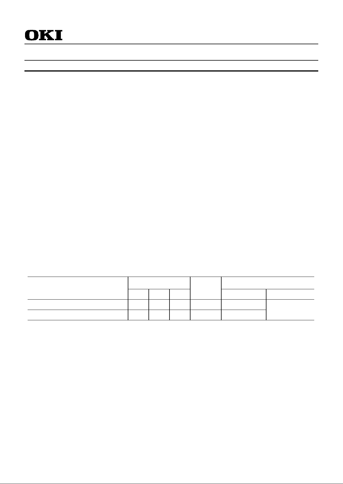
PRODUCT FAMILY
Access Time (Max. ) Power Dissipation
Family
t
RAC
t
AA
t
CAC
Cycle
Time
(Min.)
Operating (Max.) Standby (Max.)
MSC23836D-60BS20/DS20 60ns 30ns 15ns 110ns 5995mW
MSC23836D-70BS20/DS20 70ns 35ns 20ns 130ns 5500mW
110mW
Page 2
Semiconductor MSC23836D
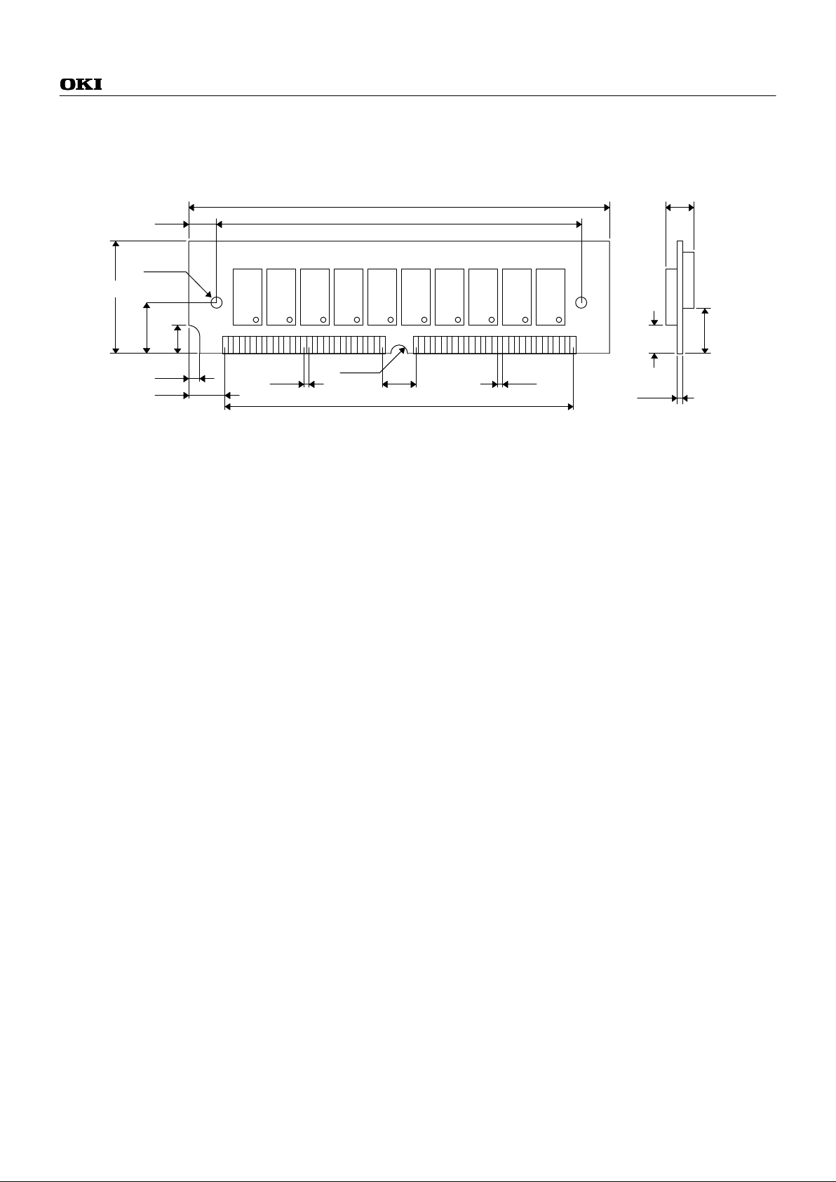
MODULE OUTLINE
1
72
R1.57
6.35
1.04Typ.
1.27±0.1
95.25
2.03Typ.
6.35Typ.
Typ.
6.35
Typ.
10.16
φ
3.18
25.4±0.2
101.19Typ.
107.95±0.2
*1
3.38Typ.
3.17Min.
5.71Min.
9.3Max.
+0.1
-0.08
1.27
(Unit : mm )
MSC23836D-xxBS20/DS20
*1 The common size difference of the board width 12.5mm of its height is specified as ±0.2.
The value above 12.5mm is specified as ±0.5.
Page 3
Semiconductor MSC23836D
PIN C ONFIGURATION
Pin No. Pin Name Pin No. Pin Nam e Pin No. Pin Nam e Pin No. Pin Nam e
1VSS19 A10 37DQ1755DQ12
2 DQ0 20 DQ4 38 DQ35 56 DQ30
3 DQ18 21 DQ22 39 V
SS
57 DQ13
4 DQ1 22 DQ5 40 /CAS0 58 DQ31
5 DQ19 23 DQ23 41 /CAS2 59 V
CC
6 DQ2 24 DQ6 42 /CAS3 60 DQ32
7 DQ20 25 DQ24 43 /CAS1 61 DQ14
8 DQ3 26 DQ7 44 /RAS0 62 DQ33
9 DQ21 27 DQ25 45 /RAS1 63 DQ15
10 V
CC
28 A7 46 NC 64 DQ34
11 NC 2 9 NC 47 /WE 65 DQ 1 6
12 A0 30 V
CC
48 NC 66 NC
13 A1 31 A8 49 DQ9 67 PD1
14 A2 32 A9 50 DQ27 68 PD2
15 A3 33 /RAS3 51 DQ10 69 PD3
16 A4 34 /RAS2 52 DQ28 70 PD4
17 A5 35 DQ26 53 DQ11 71 NC
18 A6 36 DQ8 54 DQ29 72 V
SS
Presence Detect Pins
Pin No. Pin Name
MSC23836D
-60BS20/DS20
MSC23836D
-70BS20/DS20
67 PD1 NC NC
68 PD2 V
SS
V
SS
69 PD3 NC V
SS
70 PD4 NC NC
Page 4

Semiconductor MSC23836D
BLOCK DIAGRAM
/WE
/CAS0
/RAS0
A0-A10
/CAS1
/RAS1
A0-A10
DQDQDQ0DQDQ
/OE
V
SS
/RAS
/CAS
/WE
VCCA0-A10
DQ
DQDQDQ
/OE
V
CC
/RAS
/CAS
/WE
V
SS
DQ1
DQ2
DQ3
A0-A10
DQ1
DQ8
DQ2
/OE
V
SS
/RAS
/CAS1
/WE
V
CC
A0-A10
DQ1
DQ2
/OE
V
CC
/RAS
/CAS1
/WE
V
SS
DQ17
/CAS2
/CAS2
/CAS2
/RAS2
/CAS3
/RAS3
V
CC
VSSC1-C20
A0-A10
DQ
DQ
DQDQ/OE
VCC/RAS
/CAS
/WE
V
SS
A0-A10
DQ
DQ
DQDQ/OE
VSS/RAS
/CAS
/WE
V
CC
DQ4
DQ5
DQ6
DQ7
A0-A10
DQ
DQDQDQ
/OE
V
CC
/RAS
/CAS
/WE
VSSA0-A10
DQ
DQDQDQ
/OE
V
SS
/RAS
/CAS
/WE
VCCDQ9
DQ10
DQ11
DQ12
A0-A10
DQ
DQ
DQDQ/OE
/RAS
/CAS
/WE
A0-A10
DQ
DQ
DQDQ/OE
/RAS
/CAS
/WE
DQ13
DQ14
DQ15
DQ16
A0-A10
DQDQDQ18DQDQ
/OE
/RAS
/CAS
/WE
A0-A10
DQ
DQDQDQ
/OE
/RAS
/CAS
/WE
DQ19
DQ20
DQ21
VSSVCCVCCVSSVCCVSSVSSV
CC
A0-A10
DQDQDQ22DQDQ
/OE
/RAS
/CAS
/WE
A0-A10
DQ
DQ
DQDQ/OE
/RAS
/CAS
/WE
DQ23
DQ24
DQ25
VSSVCCVCCVSSA0-A10
DQ1
DQ26
DQ2
/OE
V
SS
/RAS
/CAS1
/WE
V
CC
A0-A10
DQ1
DQ2
/OE
V
CC
/RAS
/CAS1
/WE
V
SS
DQ35
/CAS2
/CAS2
A0-A10
DQDQDQ27DQDQ
/OE
/RAS
/CAS
/WE
A0-A10
DQ
DQDQDQ
/OE
/RAS
/CAS
/WE
DQ28
DQ29
DQ30
VSSVCCVCCV
SS
A0-A10
DQDQDQ31DQDQ
/OE
/RAS
/CAS
/WE
A0-A10
DQ
DQ
DQDQ/OE
/RAS
/CAS
/WE
DQ32
DQ33
DQ34
VSSVCCVCCV
SS
Page 5

Semiconductor MSC23836D
ELECTRICAL CHARAC TERISTICS
Absolute Maximum Ratings
Parameter Symbol Rating Unit
Voltage on Any Pin Relative to V
SS
VIN, V
OUT
-0.5 to +7.0 V
Voltage on VCC Supply Relative to V
SS
V
CC
-0.5 to +7.0 V
Short Circuit Output Curr ent I
OS
50 mA
Power Dissipation PD *20W
Operating Temperature T
OPR
0 to +70 °C
Storage Temperature T
STG
-40 to +125 °C
* Ta = 25°C
Recommended Operating Conditions
( Ta = 0°C to +70°C )
Paramete r Symbol Min. Typ. Max. Unit
V
CC
4.5 5.0 5.5 V
Power Supply Voltage
V
SS
000V
Input High Voltage V
IH
2.4 - VCC + 0.5 V
Input Low Voltage V
IL
-0.5 - 0.8 V
Capacitance
( VCC = 5V ± 10%, Ta = 25°C, f = 1 MHz )
Paramete r Symbol Typ. Max. Uni t
Input Capacitance (A0 - A10) C
IN1
- 135 pF
Input Capacitance (/WE) C
IN2
- 155 pF
Input Capacitance (/RAS0- /RAS3) C
IN3
-43pF
Input Capacitance (/CAS0- /CAS3) C
IN4
-50pF
I/O Capacitance (DQ0 - DQ35) C
DQ
-26pF
Page 6

Semiconductor MSC23836D
DC CHARACTERISTICS
(VCC = 5V ± 10%, Ta = 0°C to +70°C )
MSC23836D
-60BS20/DS20
MSC23836D
-70BS20/DS20
Paramete r Symbol Conditi on
Min. Max. Min. Max.
Unit Note
Input Leakage Current I
LI
0V ≤ VIN ≤ 6.5V;
All other pins not
under test = 0V
-200 200 -200 200 µA
Output Leakage Current I
LO
DQ disable
0V ≤ V
OUT
≤ 5.5V
-20 20 -20 20 µA
Output High Voltage V
OH
IOH = -5.0mA 2.4 V
CC
2.4 V
CC
V
Output Low Voltage V
OL
IOL = 4.2mA 0 0.4 0 0.4 V
Average Power
Supply Current
(Operating)
I
CC1
/RAS, /CAS cy cling,
t
RC
= Min.
- 1090 - 1000 mA 1, 2
/RAS, /CAS = V
IH
-40-40mA1
Power supply current
(Standby)
I
CC2
/RAS, /CAS
≥ V
CC
-0.2V
-20-20mA1
Average Power
Supply Current
(/RAS only refresh)
I
CC3
/RAS cycling,
/CAS = V
IH
,
t
RC
= Min.
- 1090 - 1000 mA 1, 2
Average Power
Supply Current
(/CAS before /RAS refresh)
I
CC6
/RAS cycling,
/CAS before /RAS
- 1090 - 1000 mA 1, 2
Average Power
Supply Current
(Fast Page Mode)
I
CC7
/RAS = VIL,
/CAS cycling,
t
PC
= Min.
- 910 - 820 mA 1, 3
Notes: 1. ICC Max. is specified as ICC for output open conditi on.
2. Address can be changed once or less while /RA S = V
IL
.
3. Address can be changed once or less while /CA S = V
IH
.
Page 7

Semiconductor MSC23836D
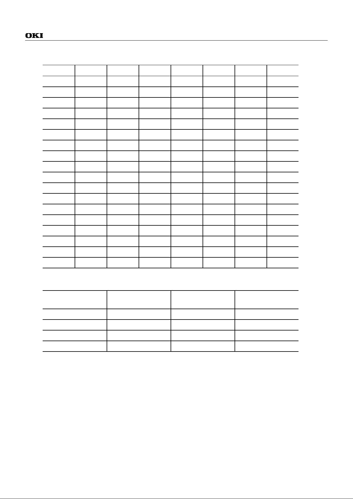
AC CHARACTERISTICS (1/ 2)
(VCC = 5V ± 10%, Ta = 0°C to +70°C ) Note: 1, 2, 3, 9, 10
MSC23836D
-60BS20/DS20
MSC23836D
-70BS20/DS20
Paramete r Symbol
Min. Max. Min. Max.
Unit Note
Random Read or Writ e Cycle Time t
RC
110 - 130 - ns
Fast Page Mode Cycle Time t
PC
40 - 45 - ns
Access Time from /RAS t
RAC
- 60 - 70 ns 4, 5, 6
Access Time from /CAS t
CAC
- 15 - 20 ns 4, 5
Access Time from Column Address t
AA
- 30 - 35 ns 4, 6
Access Time from /CAS Precharge t
CPA
- 35 - 40 ns 4
Output Low Impedance Time from /CAS t
CLZ
0-0-ns4
/CAS to Data Output Buffer Turn-off Delay Time t
OFF
0 15 0 20 ns 7
Transition Time t
T
3 50 3 50 ns 3
Refresh Period t
REF
-32-32ms
/RAS Precharge Tim e t
RP
40 - 50 - ns
/RAS Pulse Width t
RAS
60 10K 70 10K ns
/RAS Pulse Width ( Fast Page Mode) t
RASP
60 100K 70 100K ns
/RAS Hold Time t
RSH
15 - 20 - ns
/CAS Precharge Time (Fast Page Mode) t
CP
10 - 10 - ns
/CAS Pulse Width t
CAS
15 10K 20 10K ns
/CAS Hold Time t
CSH
60 - 70 - ns
/CAS to /RAS Pr echarge Time t
CRP
10 - 10 - ns
/RAS Hold Time from /CAS Precharge t
RHCP
35 - 40 - ns
/RAS to /CAS Delay Time t
RCD
20 45 20 50 ns 5
/RAS to Column Address Delay Time t
RAD
15 30 15 35 ns 6
Row Address Set-up Time t
ASR
0-0-ns
Row Address Hol d Time t
RAH
10 - 10 - ns
Column Address Set-up Time t
ASC
0-0-ns
Column Address Hol d Time t
CAH
15 - 15 - ns
Column Address to /RAS Lead Time t
RAL
30 - 35 - ns
Read Command Set-up Time t
RCS
0-0-ns
Read Command Hold Time t
RCH
0-0-ns8
Read Command Hold Time referenced to /RAS t
RRH
0-0-ns8
Page 8

Semiconductor MSC23836D
AC Characteristics (2/2)
(VCC = 5V ± 10%, Ta = 0°C to +70°C ) Note: 1, 2, 3, 9, 10
MSC23836D
-60BS20/DS20
MSC23836D
-70BS20/DS20
Paramete r Symbol
Min. Max. Min. Max.
Unit Note
Writ e Command Set-up Time t
WCS
0-0-ns
Writ e Command Hold Time t
WCH
10 - 15 - ns
Writ e Command Pulse Wi dth t
WP
10 - 10 - ns
Writ e Command to /RAS Lead Time t
RWL
15 - 20 - ns
Writ e Command to /CAS Lead Time t
CWL
15 - 20 - ns
Data-in Set-up Time t
DS
0-0-ns
Data-i n Ho ld Time t
DH
15 - 15 - ns
/CAS Active Delay Time from /RAS Precharge t
RPC
10 - 10 - ns
/RAS to /CAS Set-up Time
(/CAS before /RAS)
t
CSR
10 - 10 - ns
/RAS to /CAS Hold Time
(/CAS before /RAS)
t
CHR
20 - 20 - ns
/WE to /RAS Precharge Time
(/CAS before /RAS)
t
WRP
10 - 10 - ns
/WE Hold Time from /RAS
(/CAS before /RAS)
t
WRH
10 - 10 - ns
/RAS to /WE Set-up Time
(Test Mode)
t
WTS
10 - 10 - ns
/RAS to /WE Hold Time
(Test Mode)
t
WTH
20 - 20 - ns
Page 9

Semiconductor MSC23836D
Notes: 1. A start-up delay of 200µs is required after power-up, followed by a minimum of eight initialization cycles
(/RAS only r efresh or /CAS before /RAS refresh) befor e pr oper devic e oper ation is achieved.
2. The AC characteristic s assumes t
T
= 5ns.
3. V
IH
(Min.) and VIL(Max.) are ref erence lev els f or m easuring input tim ing signals. Transiti on ti me (tT) are
measured between V
IH
and VIL.
4. This parameter is m easured wit h a load circuit equivalent t o 2TTL loads and 100pF.
5. Operation within the t
RCD
(Max.) limit ensures that t
RAC
(Max.) can be met.
t
RCD
(Max.) is specified as a reference point only. If t
RCD
is greater than the specified t
RCD
(Max.) limit, then
the access tim e is controll ed by t
CAC
.
6. Operation within the t
RAD
(Max.) limit ensures that t
RAC
(Max.) can be met.
t
RAD
(Max.) is specified as a reference point only. If t
RAD
is greater than the specified t
RAD
(Max.) limit, then
the access tim e is controll ed by t
AA
.
7. t
OFF
(Max.) define the time at which the output achieves the open circuit condition and are not referenced
to output voltage levels.
8. t
RCH
or t
RRH
must be satisfi ed for a read cycle.
9. The test mode is initiated by perf orming a /WE and /CAS before /RAS ref resh cycle. This mode is
latched and remains in effect until the exit cycle is generated. The test mode specified in this data sheet
is an 8-bit parallel test function. CA0, CA1 and CA10 are not used. In a read cycle, if all int ernal bits are
equal, the DQ pin will indica te a h igh le vel. If an y in ter na l b its ar e n o t equal, the DQ pin will indicat e a low
level. The test mode is cleared and the memory devic e retur ned to its normal operating state by a /RAS
only refresh or /CAS before /RAS refresh cycle.
10. In a test mode read cycle, the value of access time parameters is delayed for 5ns for the specified value.
These parameters should be specifi ed in test m ode cycle by adding the abov e v alue t o the specif ied
value in this data sheet.
 Loading...