

Datasheet MSC2343257A-60BS8, MSC2343257A-60DS8, MSC2343257A-70BS8, MSC2343257A-70DS8 Datasheet (OKI)
Page 1
¡ Semiconductor
MSC2343257A-xxBS8/DS8
¡ Semiconductor
MSC2343257A-xxBS8/DS8
4,194,304-Word ¥ 32-Bit DRAM MODULE : FAST PAGE MODE TYPE WITH EDO
1
DESCRIPTION
The Oki MSC2343257A-xxBS8/DS8 is a fully decoded 4,194,304-word ¥ 32-bit CMOS dynamic
random access memory composed of eight 16-Mb DRAMs (4M ¥ 4) in SOJ. The mounting of eight
DRAMs together with decoupling capacitors on a 72-pin glass epoxy SIMM Package supports
any application where high density and large capacity of storage memory are required.
FEATURES
• 4,194,304-word ¥ 32-bit organization
• 72-pin SIMM
MSC2343257A-xxBS8 : Gold tab
MSC2343257A-xxDS8 : Solder tab
• Single 5 V supply ±10% tolerance
• Input : TTL compatible
• Output : TTL compatible, 3-state, nonlatch
• Refresh : 2048 cycles/32 ms
• CAS before RAS refresh, CAS before RAS hidden refresh, RAS-only refresh capability
• Multi-bit test mode capability
• Fast Page Mode with EDO capability
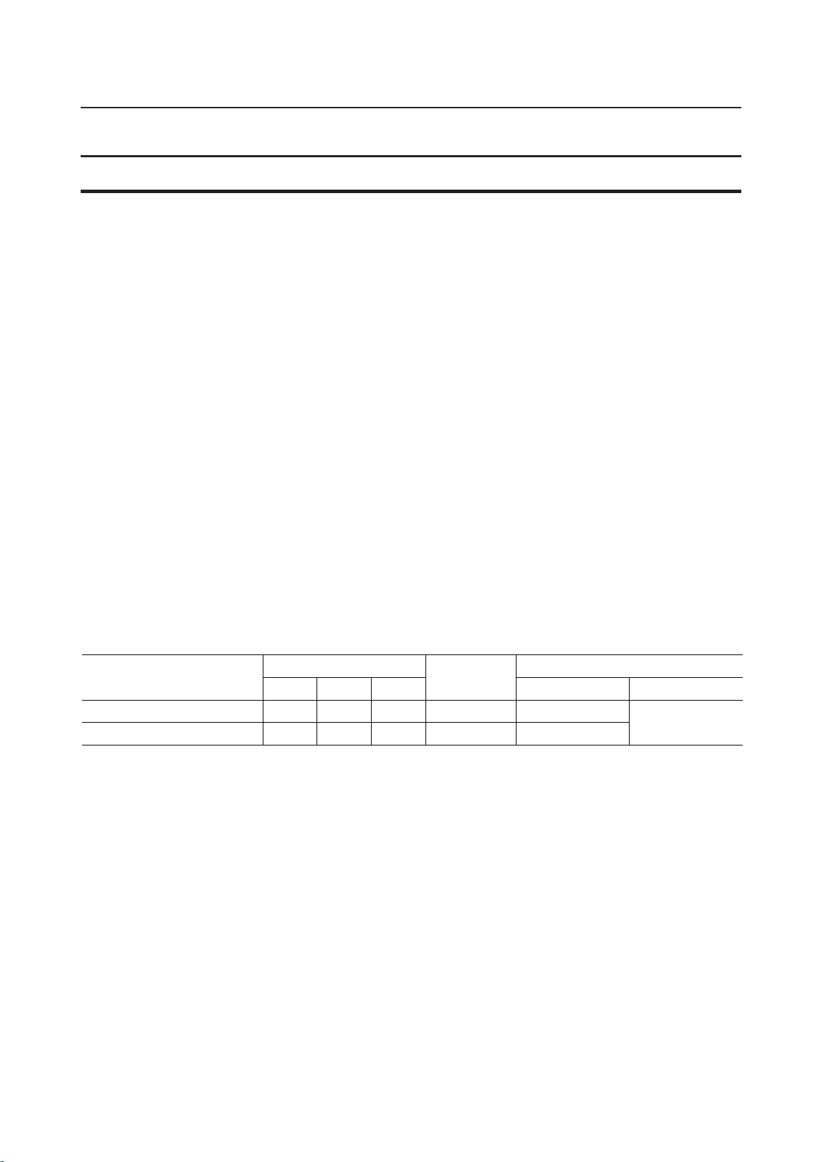
PRODUCT FAMILY
Family
MSC2343257A-60BS8/DS8 5280 mW
MSC2343257A-70BS8/DS8 4840 mW
Access Time (Max.)
t
RAC
60 ns 30 ns 15 ns 110 ns
70 ns 35 ns 20 ns 130 ns
t
AA
t
CAC
Cycle Time
(Min.)
Operating (Max.)
Power Dissipation
Standby (Max.)
44 mW
101
Page 2
MSC2343257A-xxBS8/DS8 ¡ Semiconductor
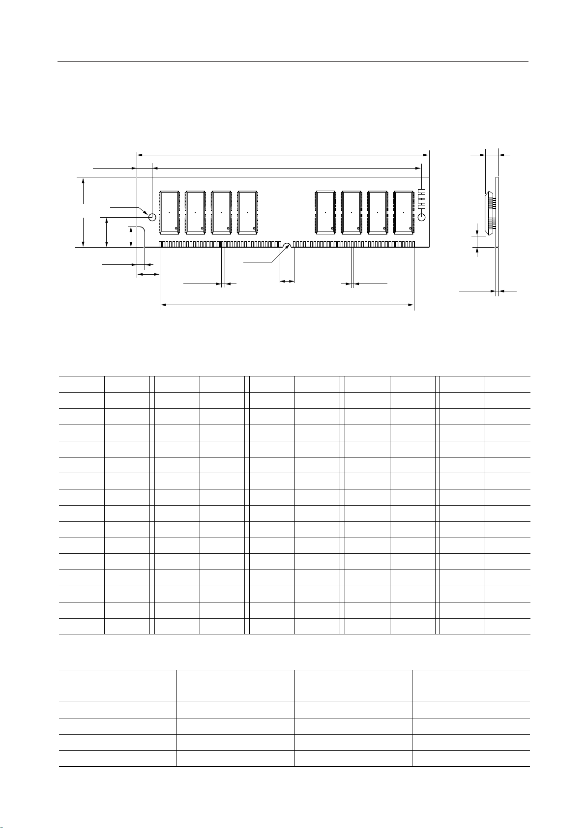
PIN CONFIGURATION
MSC2343257A-xxBS8/DS8
(Unit : mm)
25.4 ±0.2
Typ.
10.16
3.18φ
Typ.
6.35
2.03 Typ.
* 1
107.95 ±0.2
101.19 Typ.3.38 ±0.2
1
72
3.7 Min.
R1.57
5.28 Max.
6.35 Typ.
1.27 ±0.1
6.35
1.04 Typ.
95.25
*1 The common size difference of the board width 12.5 mm of its height is
specified as ±0.2. The value above 12.5 mm is specified as ±0.5.
Pin No.
Pin Name
Pin No.
Pin Name
Pin No.
Pin Name
1VSS16 A4 31 A8
Pin No.
46 NC
2 DQ0 17 A5 32 A9 47 WE
3 DQ16 18 A6 33 NC 48 NC
4 DQ1 19 A10 34 RAS2 49 DQ8
5 DQ17 20 DQ4 35 NC 50 DQ24
6 DQ2 21 DQ20 36 NC 51 DQ9
7 DQ18 22 DQ5 37 NC 52 DQ25
8 DQ3 23 DQ21 38 NC 53 DQ10
9 DQ19 24 DQ6 39 V
10 V
CC
25 DQ22 40 CAS0 55 DQ11
SS
54 DQ26
11 NC 26 DQ7 41 CAS2 56 DQ27
12 A0 27 DQ23 42 CAS3 57 DQ12
13 A1 28 A7 43 CAS1 58 DQ28
14 A2 29 NC 44 RAS0 59 V
15 A3 30 Vcc 45 NC 60 DQ29
Pin Name
CC
+0.1
1.27
–0.08
Pin No.
61 DQ13
62 DQ30
63 DQ14
64 DQ31
65 DQ15
66 NC
67 PD1
68 PD2
69 PD3
70 PD4
71 NC
72 V
Pin Name
SS
Presence Detect Pins
Pin No.
67 PD1
68 PD2
69 PD3
70 PD4
102
Pin Name
-60BS8/DS8
V
SS
NC
NC
NC
MSC2343257AMSC2343257A
-70BS8/DS8
V
SS
NC
V
SS
NC
Page 3
¡ Semiconductor
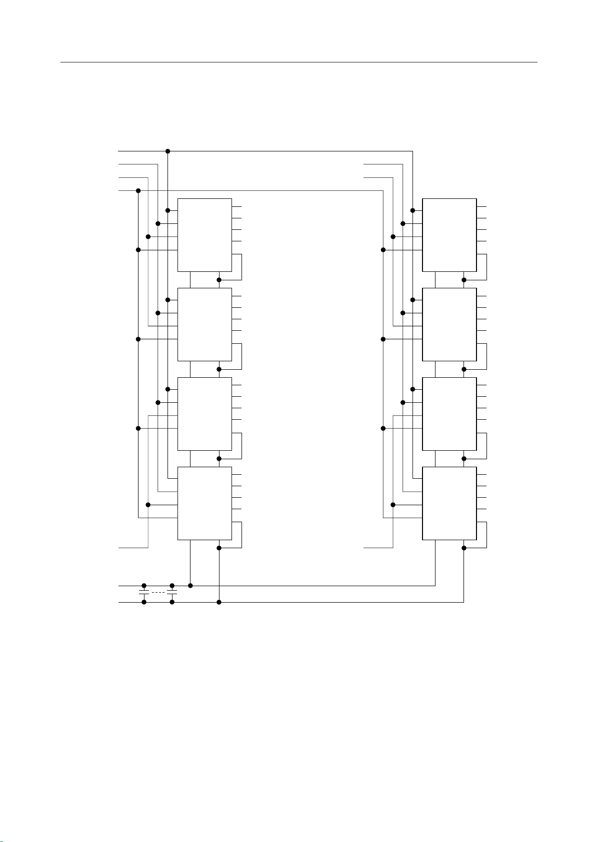
BLOCK DIAGRAM
MSC2343257A-xxBS8/DS8
A0 - A10
RAS0
CAS0
WE
A0 - A10
RAS
CAS
WE
V
CC
A0 - A10
RAS
CAS
WE
V
CC
A0 - A10
RAS
CAS
WE
V
CC
DQ
DQ
DQ
DQ
V
DQ
DQ
DQ
DQ
V
DQ
DQ
DQ
DQ
V
OE
OE
OE
RAS2
1
CAS2
DQ0
DQ1
DQ2
DQ3
A0 - A10
RAS
CAS
WE
SS
DQ4
DQ5
DQ6
DQ7
V
A0 - A10
RAS
CAS
WE
SS
DQ8
DQ9
DQ10
DQ11
V
A0 - A10
RAS
CAS
WE
SS
V
DQ
DQ16
DQ
DQ17
DQ
DQ18
DQ
DQ19
OE
V
CC
DQ
DQ
DQ
DQ
SS
DQ20
DQ21
DQ22
DQ23
OE
CC
V
SS
DQ
DQ24
DQ
DQ25
DQ
DQ26
DQ
DQ27
OE
CC
V
SS
CAS1
V
V
CC
C1 C8
SS
A0 - A10
RAS
CAS
WE
V
CC
DQ
DQ
DQ
DQ
V
OE
DQ12
DQ13
DQ14
DQ15
A0 - A10
RAS
CAS
WE
SS
V
DQ
DQ28
DQ
DQ29
DQ
DQ30
DQ
DQ31
OE
CC
V
SS
CAS3
103
Page 4

MSC2343257A-xxBS8/DS8 ¡ Semiconductor
ELECTRICAL CHARACTERISTICS
Absolute Maximum Ratings
Parameter
Voltage on Any Pin Relative to V
Voltage V
Supply Relative to V
CC
Short Circuit Output Current
Power Dissipation
Operating Temperature
Storage Temperature
SS
SS
Symbol
VIN, V
OUT
V
CC
I
OS
P
D
T
opr
T
stg
Rating Unit
–1.0 to 7.0 V
–1.0 to 7.0 V
50 mA
8W
0 to 70 °C
–40 to 125 °C
Note: Permanent device damage may occur if ABSOLUTE MAXIMUM RATINGS are
exceeded. Functional operation should be restricted to the conditions as detailed in the
operational sections of this data sheet. Exposure to absolute maximum rating conditions
for extended periods may affect device reliability.
Recommended Operating Conditions
(Ta = 0°C to 70°C)
Parameter
Power Supply Voltage
Input High Voltage
Input Low Voltage
Symbol
V
CC
V
SS
V
IH
V
IL
Min.
Typ.
4.5 5.0 5.5 V
000V
2.4 — 6.5 V
–1.0 — 0.8 V
Max.
Unit
Capacitance
Parameter
Symbol
C
IN1
C
IN2
C
IN3
C
IN4
C
DQ
Typ.
—57
Note : Capacitance measured with Boonton Meter.
Max.
(Ta = 25°C, f = 1 MHz)
Unit
pFInput Capacitance (A0 - A10)
pFInput Capacitance (WE)—65
pFInput Capacitance (RAS0, RAS2)—35
pFInput Capacitance (CAS0 - CAS3)—20
pFI/O Capacitance (DQ0 - DQ31) — 16
104
Page 5

¡ Semiconductor
MSC2343257A-xxBS8/DS8
DC Characteristics
Parameter
Input Leakage Current
Output Leakage Current
Output High Voltage
Output Low Voltage
Average Power
Supply Current
(Operating)
Power Supply
Current (Standby)
Average Power
Supply Current
(RAS-only Refresh)
Average Power
Supply Current
(CAS before RAS Refresh)
Average Power
Supply Current
(Fast Page Mode)
Symbol
I
LI
I
LO
V
OH
V
OL
I
CC1
I
CC2
I
CC3
I
CC6
I
CC7
Condition
0 V £ VI £ 6.5 V;
All other pins not
under test = 0 V
disable
D
OUT
0 V £ V
I
OH
I
OL
£ 5.5 V
O
= –5.0 mA
= 4.2 mA
RAS, CAS cycling,
= Min.
t
RC
RAS, CAS = V
IH
RAS, CAS
≥ V
–0.2 V
CC
RAS cycling,
= Min.
,
IH
CAS = V
t
RC
RAS cycling,
CAS before RAS,
= Min.
t
RC
RAS = V
,
IL
CAS cycling,
= Min.
t
HPC
MSC2343257A
-60BS8/DS8
Min.
–80
–10
2.4
0
—
—
—
—
—
—
Max.
80
10
V
CC
0.4
960
16
8
960
960
1120
(VCC = 5 V ±10%, Ta = 0°C to 70°C)
MSC2343257A
-70BS8/DS8
Min.
–80
–10
2.4
0
—
—
—
—
—
—
Max.
80
10
V
CC
0.4
880
16
8
880
880
1040
Unit
1
µA
µA
V
V
mA
mA
mA
mA
mA
mA
Note
1, 2
1
1
1, 2
1, 2
1, 3
Notes: 1. ICC Max. is specified as ICC for output open condition.
2. Address can be changed once or less while RAS=VIL.
3. Address can be changed once or less while CAS=VIH.
105
Page 6

MSC2343257A-xxBS8/DS8 ¡ Semiconductor
AC Characteristics (1/2)
Parameter
Random Read or Write Cycle Time
Fast Page Mode Cycle Time t
Access Time from RAS t
Access Time from CAS t
Access Time from Column Address t
Access Time from CAS Precharge t
Output Low Impedance Time from CAS t
Output Hold Time from CAS Low t
CAS to Data Output Buffer Turn-off Delay Time
RAS to Data Output Buffer Turn-off Delay Time
WE to Data Output Buffer Turn-off Delay Time
Transition Time t
Refresh Period t
RAS Precharge Time t
RAS Pulse Width t
RAS Pulse Width (Fast Page Mode) t
RAS Hold Time t
CAS Precharge Time t
CAS Pulse Width t
RAS Low to CAS High Delay Time t
CAS High to RAS Low Delay Time t
RAS Hold Time from CAS Precharge t
RAS to CAS Delay Time t
RAS to Column Address Delay Time t
RAS to Second CAS Delay Time t
Row Address Set-up Time t
Row Address Hold Time t
Column Address Set-up Time t
Column Address Hold Time t
Column Address Hold Time from RAS t
Column Address to RAS Lead Time t
Symbol
t
RC
HPC
RAC
CAC
AA
CPA
CLZ
DOH
t
CEZ
t
REZ
t
WEZ
T
REF
RP
RAS
RASP
RSH
CP
CAS
CSH
CRP
RHCP
RCD
RAD
RSCD
ASR
RAH
ASC
CAH
AR
RAL
(V
= 5 V ±10%, Ta = 0°C to 70°C) Note 1,2,3,10,11
CC
MSC2343257A
-60BS8/DS8
Min.
110
25
—
—
—
—
0
0
2
—
40
60
60
15
10
10
40
10
35
20
15
0
10
0
10
40
30
Max.
—
—
60
15
30
35
—
15
50
32
—
10k
100k
—
—
10k
—
—
—
45
30
—
—
—
—
—
—
MSC2343257A
-70BS8/DS8
Min.
130
30
—
—
—
—
0
0
2
—
50
70
70
20
10
10
45
10
40
20
15
0
10
0
15
45
35
Max.
—
—
70
20
35
40
—
20
50
32
—
10k
100k
—
—
10k
—
—
—
50
35
—
—
—
—
—
—
Unit
ns
ns
ns
ns
ns
ns
ns
ns5—5—
ns
ns 7, 8020015
ns 7020015
ns
ms
ns
ns
ns
ns
ns
ns
ns
ns
ns
ns
ns
ns70 —60 —
ns
ns
ns
ns
ns
ns
Note
4, 5, 6
4, 5
4, 6
4
4
7, 8
3
5
6
106
Page 7

¡ Semiconductor
MSC2343257A-xxBS8/DS8
AC Characteristics (2/2)
Parameter
Read Command Set-up Time
Read Command Hold Time
Read Command Hold Time referenced to RAS
Write Command Set-up Time
Write Command Hold Time
Write Command Hold Time from RAS
Write Command Pulse Width
Write Command Pulse Width (Output Disable)
Write Command to RAS Lead Time
Write Command to CAS Lead Time
Data-in Set-up Time
Data-in Hold Time
Data-in Hold Time from RAS
CAS Active Delay Time from RAS Precharge
RAS to CAS Set-up Time (CAS before RAS)
RAS to CAS Hold Time (CAS before RAS)ns
WE to RAS Precharge Time (CAS before RAS)
WE Hold Time from RAS (CAS before RAS)
RAS to WE Set-up Time (Test Mode)
RAS to WE Hold Time (Test Mode)
Symbol
RCS
t
RCH
t
RRH
t
WCS
t
WCH
t
WCR
t
WP
t
WPE
t
RWL
t
CWL
t
DS
t
DH
t
DHR
t
RPC
t
CSR
t
CHR
t
WRP
t
WRH
t
WTS
t
WTH
(V
= 5 V ±10%, Ta = 0°C to 70°C) Note 1,2,3,10,11
CC
MSC2343257A
-60BS8/DS8
Min.
0
0
0
0
10
45
10
15
15
0
15
40
10
10
20
Max.
—
—
—
—
—
—
—
—
—
—
—
—
—
—
—
MSC2343257A
-70BS8/DS8
Min.
0
0
0
0
15
50
10
20
20
0
15
45
10
10
20
Max.
—t
—
—
—
—
—
—
—
—
—
—
—
—
—
—
Unit
ns
ns
ns
ns
ns
ns
ns
ns10 —5—
ns
ns
ns
ns
ns
ns
ns
ns10 —10 —
ns10 —10 —
ns10 —10 —
ns20 —20 —
Note
1
9
9
107
Page 8

MSC2343257A-xxBS8/DS8 ¡ Semiconductor
Notes: 1. A start-up delay of 200 µs is required after power-up, followed by a minimum of eight
initialization cycles (RAS-only refresh or CAS before RAS refresh) before proper device
operation is achieved.
2. The AC characteristics assume tT = 5 ns.
3. VIH (Min.) and VIL (Max.) are reference levels for measuring input timing signals.
Transition times (tT) are measured between VIH and VIL.
4. This parameter is measured with a load circuit equivalent to 2 TTL loads and 100 pF.
5. Operation within the t
t
(Max.) is specified as a reference point only. If t
RCD
t
(Max.) limit, access time is controlled by t
RCD
6. Operation within the t
t
(Max.) is specified as a reference point only. If t
RAD
t
(Max.) limit, access time is controlled by tAA.
RAD
7. t
CEZ
(Max.), t
(Max.) and t
REZ
(Max.) limit ensures that t
RCD
(Max.) limit ensures that t
RAD
(Max.) define the time at which the output achieves
WEZ
CAC
(Max.) can be met.
RAC
is greater than the specified
RCD
.
(Max.) can be met.
RAC
is greater than the specified
RAD
the open circuit condition and are not referenced to output voltage levels.
8. t
9. t
CEZ
RCH
and t
or t
must be satisfied for open circuit condition.
REZ
must be satisfied for a read cycle.
RRH
10. The test mode is initiated by performing a WE and CAS before RAS refresh cycle.
This mode is latched and remains in effect until the exit cycle is generated.
The test mode specified in this data sheet is an 8-bit parallel test function. CA0, CA1
and CA10 are not used. In a read cycle, if all internal bits are equal, the DQ pin will
indicate a high level. If any internal bits are not equal, the DQ pin will indicate a low
level. The test mode is cleared and the memory device returned to its normal
operating state by performing a RAS-only refresh cycle or a CAS before RAS refresh
cycle.
The 4M ¥ 32 module can be tested as an 1M ¥ 32 module in this test mode.
108
11. In a test mode read cycle, the access time parameters are delayed by 5 ns. The test
mode parameters are obtained by adding 5 ns to the normal read cycle values.
See ADDENDUM I for AC Timing Waveforms
 Loading...