

Page 1

E2C0011-27-Y4
¡ Semiconductor MSC1164
¡ Semiconductor
This version: Nov. 1997
Previous version: Jul. 1996
MSC1164
20-Bit Grid/Anode Driver
GENERAL DESCRIPTION
The MSC1164 is a monolithic IC using the Bi-CMOS process technology for hybridizing CMOS
and bipolar transistors on the same chip. The logic portion such as the input stage, shift register
and latch is fabricated by CMOS and the output driver requiring a high withstand voltage is
fabricated by bipolar transistors.
Since a 32-pin plastic SSOP package is used, the display unit size can be reduced.
FEATURES
The MSC1164 is designed as a VFD grid/anode driver with emitter-follower force output with
20-bit active pull-down and built-in 20-bit shift register and latch.
• Logic Supply Voltage (VCC):5V
• Driver Supply Voltage (VHV) : 65V
• Driver Output Current
I
OHVH1
I
OHVH2
I
OHVL
• 20-bit output (with latch circuit)
• 20-bit shift register
• Clock frequency : 4MHz
• Package options:
32-pin plastic SSOP (SSOP32-P-430-1.00-K) (Product name: MSC1164GS-K)
30-pin plastic shrink DIP (SDIP30-P-400-1.78) (Product name: MSC1164SS)
:–40mA (Only one driver output: "H")
:–2mA (All driver outputs: "H")
:2mA
1/13
Page 2

¡ Semiconductor MSC1164
BLOCK DIAGRAM
CLK DIN LS
D
R-1
R-2
11
22
CHG CL
V
CC
V
HV
HVO1
HVO2
20-Bit Shift Register
20 20R-20
Q
DOUT
20-Bit Latch
HVO20
GND
2/13
Page 3

¡ Semiconductor MSC1164
INPUT AND OUTPUT CONFIGURATION
Schematic Diagrams of Logic Portion Input and Output Circuits
Input Pin
Output Pin
INPUT
V
CC
GND
V
CC
V
CC
V
CC
GND
GND
Schematic Diagram of Driver Output Circuit
V
HV
DOUT
GND
V
HV
HVO
GND
GND
3/13
Page 4

¡ Semiconductor MSC1164
PIN CONFIGURATION (TOP VIEW)
NC
NC
DOUT
LS
CL
V
CC
HVO20
HVO19
HVO18
HVO17
HVO16
HVO15
HVO14
HVO13
HVO12
HVO11
10
11
12
13
14
15
16
1
2
3
4
5
6
7
8
9
32
31
30
29
28
27
26
25
24
23
22
21
20
19
18
17
NC
CHG
DIN
CLK
GND
V
HV
HVO1
HVO2
HVO3
HVO4
HVO5
HVO6
HVO7
HVO8
HVO9
HVO10
NC: No-connection pin
32-Pin Plastic SSOP
NC 1 CHG30
DOUT 2 DIN29
LS 3 CLK28
CL 4 GND27
VCC5V
26
HV
HVO20 6 HVO125
HVO19 7 HVO224
HVO18 8 HVO323
HVO17 9 HVO422
HVO16 10 HVO521
HVO15 11 HVO620
HVO14 12 HVO719
HVO13 13 HVO818
HVO12 14 HVO917
HVO11 15 HVO1016
NC: No-connection pin
30-Pin Plastic Shrink DIP
4/13
Page 5
¡ Semiconductor MSC1164
PIN DESCRIPTION
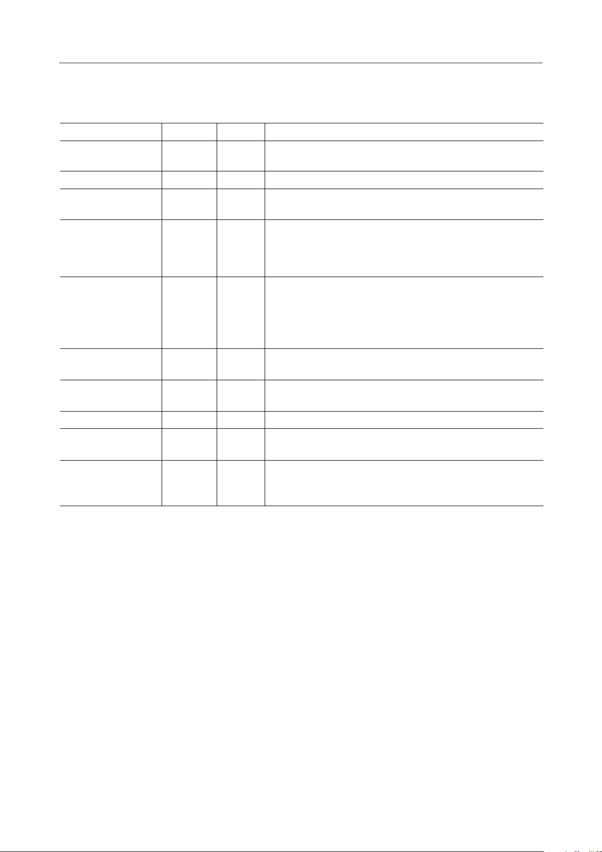
Pin SymbolFunction Description
Driver Output Driver output pin, applicable to each bit of shift register.
Driver Power Supply Power supply pin for driver circuit.
Driver GND
Logic GND
26 - 7
27 V
28
HVO1 HVO20
HV
GND
GND pin for the driver circuit.
GND pin for the logic circuit.
Clear input pin with pull-up resistor. Normally "H" level. In this
CLClear Input 5
condition, the driver outputs "H" or "L" according to the
corresponding latch output level. Setting this pin to "L" enables
the driver output to be fixed at "L" irrespective of latch output.
Latch strobe input pin with neither pull-up nor pull-down resistor.
When LS is "H", the output of the shift register becomes that of the
LSLatch Strobe Input 4
latch circuit.
When LS is "L", the latch circuit holds the contents of the shift
register that are immediately before LS goes "L".
Shift register input pin with neither pull-up nor pull-down resistor.
Display data is input in synchronization with clock. (Positive Logic)
Power supply pin for logic (except driver).
V
should be 4.5V to 5.5V.
CC
Logic Power Supply
30 DINData Input
6
V
CC
3 DOUTData Output Serial output pin for shift register.
29 CLKClock Input
Clock input pin. Data of shift register is shifted from one stage to
the next at the rising edge of clock.
Test input pin with a pull-down resistor. Normally "L". If CL = "H"
31 CHGTest Input
in this condition, the driver outputs "H" or "L" according to the
corresponding latch output.
Note: Pin numbers shown are for 32-pin plastic SSOP.
5/13
Page 6
¡ Semiconductor MSC1164
ABSOLUTE MAXIMUM RATINGS
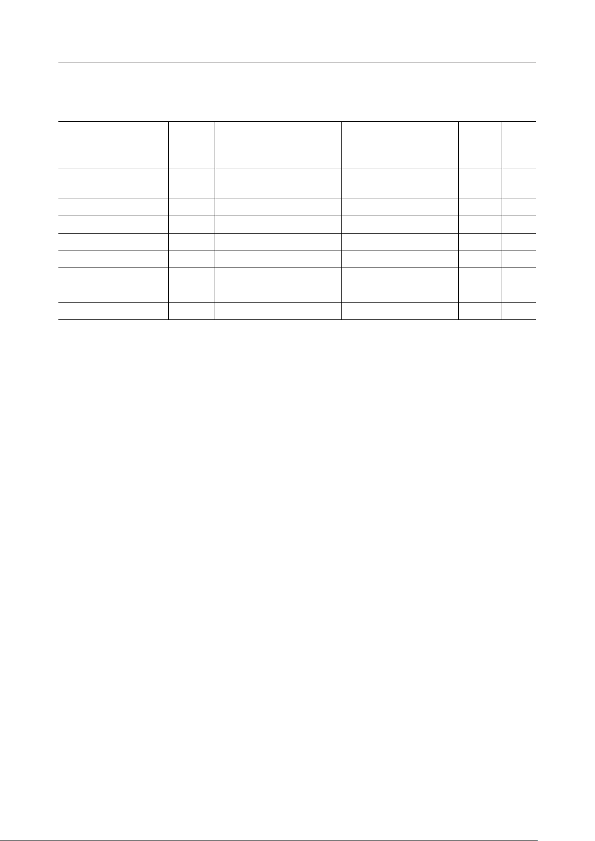
Parameter Symbol Condition Rating Unit Note
Logic Supply Voltage V
Driver Supply Voltage V
Input Voltage V
Data Output Voltage V
Driver Driving Frequency f
Power Dissipation P
CC
HV
IN
OD
DRV
D
Applicable to logic supply
voltage pin
Applicable to driver supply
voltage pin
Applicable to all input pins
Applicable to data output pin
Thermal Resistance of
R
Package
Storage Temperature T
j-a
STG
Notes: 1) Maximum Supply Voltage with respect to GND
2) Stresses beyond "Absolute Maximum Rating" may cause permanent damage to the
device.
3) Thermal resistance of the package (between junction and atmosphere)
The junction temperature (Tj) expressed by the equation below must not exceed
150˚C.
Tj=P ¥ Rj–a+Ta (P: Maximum power consumption)
–0.3 to +65 V 1
VCC to 70 V 1, 2
–0.3 to VCC +0.3 V 1
–0.3 to VCC +0.3 V 1
0 to 15 kHz —Duty cycle 50% max
790
mW —Ta £ 25°C
158 °C/W 3—
–55 to +150 °C ——
6/13
Page 7
¡ Semiconductor MSC1164
RECOMMENDED OPERATING CONDITIONS
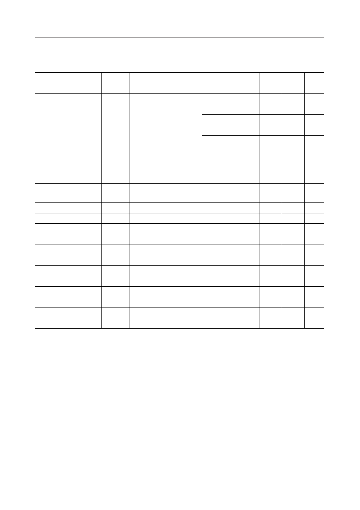
Parameter Symbol Condition Max. Unit
Logic Supply Voltage V
High Level Input Voltage V
Low Level Input Voltage V
High Level Driver Output
Current
High Level Driver Output
Current
I
OHVH1
OHVH2
Low Level Driver Output
Current
CLK Frequency f
CLK Pulse Width t
Data in Setup Time t
Data in Hold Time t
LS Pulse Width t
CLK-LS Delay Time t
LS-CLK Delay Time t
LS-CHG Delay Time t
LS-CL Delay Time t
CHG Pulse Width t
WCHG
CL Pulse Width t
Operating Temperature T
CC
HV
IH
IL
OHVL
f
WCLK
DS
DH
WLS
DCL
DLC
DLCG
DLCL
WCL
op
Applicable to logic supply voltage pin
Applicable to driver supply voltage pinDriver Supply Voltage V
Applicable to all input pins
Applicable to all input pins
Only one driver output is High
Other driver outputs are High
All driver output pins are HighI
Applicable to all driver output pinsI
See timing diagram
See timing diagram
See timing diagram
See timing diagram
See timing diagram
See timing diagram
See timing diagram
See timing diagram
See timing diagram
See timing diagram
See timing diagram
—
Min.
4.5
VCC=4.5V —V3.6
=5.5V —V4.4
V
CC
=4.5V 0.9 V—
V
CC
=5.5V 1.1 V—
V
CC
5.5 V
65 V10
–40 mA—
–2 mA—
2mA—
4 MHz—
—ns75
—ns50
—ns50
—ns80
—ns50
—ns0
— ms0
— ms0
— ms2
— ms2
85 °C–40
7/13
Page 8
¡ Semiconductor MSC1164
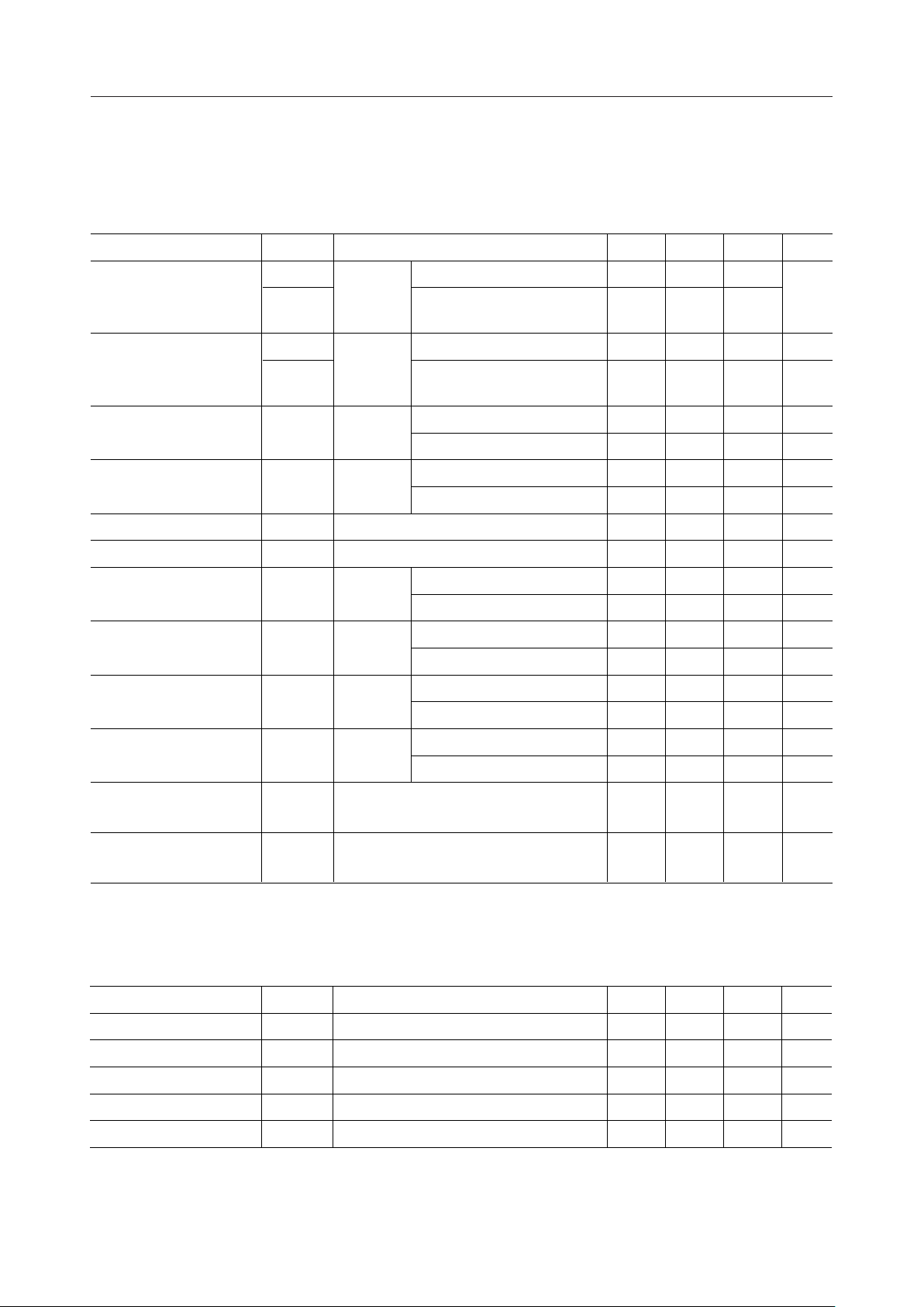
ELECTRICAL CHARACTERISTICS
DC Characteristics
(V
=5V±10%, VHV=10V to 65V, Ta=–40°C to +85°C)
CC
Parameter Symbol Condition Max. Unit
Min.
Typ.
Logic Supply Current
Driver Supply Current
High Level Input Voltage
Low Level Input Voltage
Input Capacitance C
High Level Data Output
Voltage
Low Level Data Output
Voltage
High Level Data Output
Voltage
Low Level Data Output
Voltage
V
V
V
V
I
CC1
I
CC2
I
HV1
I
HV2
V
IH
V
IL
IN
IN
ODH1
ODL1
ODH2
ODL2
No load
V
=5.5V
CC
No load
V
=5.5V
CC
—
—
IO=–20mA
I
=20mA
O
IO=–0.1mA
I
=0.1mA
O
All input: Low
All input: High, All
driver output: High, Ta=25°C
All driver output: Low
All driver output:
High, Ta=25°C
V
=4.5V ——3.15
CC
V
=5.5V ——3.85
CC
VCC=4.5V 1.35——
V
=5.5V 1.65——
CC
Ta=25°CInput Leakage Current I
Ta=25°C
=4.5V ——4.2
V
CC
V
=5.5V ——5.2
CC
VCC=4.5V 0.2——
V
=5.5V 0.2——
CC
V
=4.5V ——3.5
CC
V
=5.5V ——4.5
CC
VCC=4.5V 1.1——
V
=5.5V 1.1——
CC
—
—
2.3
—
3.4
1.00.5—
1
2.01.3—
±1 mA——
—pF15—
mA
mA
mA
V
V
V
V
V
V
V
V
V
V
V
V
High Level Driver Output
Voltage
Low Level Driver Output
Voltage
AC Characteristics
Parameter Symbol Remarks Max. UnitTyp.Min.
CLK-DOUT Delay Time t
Delay Time Low to High t
Transit Time Low to High t
Delay Time High to Low t
Transit Time High to Low t
OHVH
OHVL
PD
DLH
TLH
DHL
THL
I
=–40mAV
OHV
I
=2mAV
OHV
See timing diagram and test circuit
See timing diagram and test circuit
See timing diagram and test circuit
See timing diagram and test circuit
See timing diagram and test circuit
—V—VHV–4
3.0 V——
(V
=5V, VHV=65V, Ta=25°C)
CC
150 ns100—
1 ms0.3—
5 ms2—
1 ms0.3—
5 ms2—
8/13
Page 9
¡ Semiconductor MSC1164
9/13
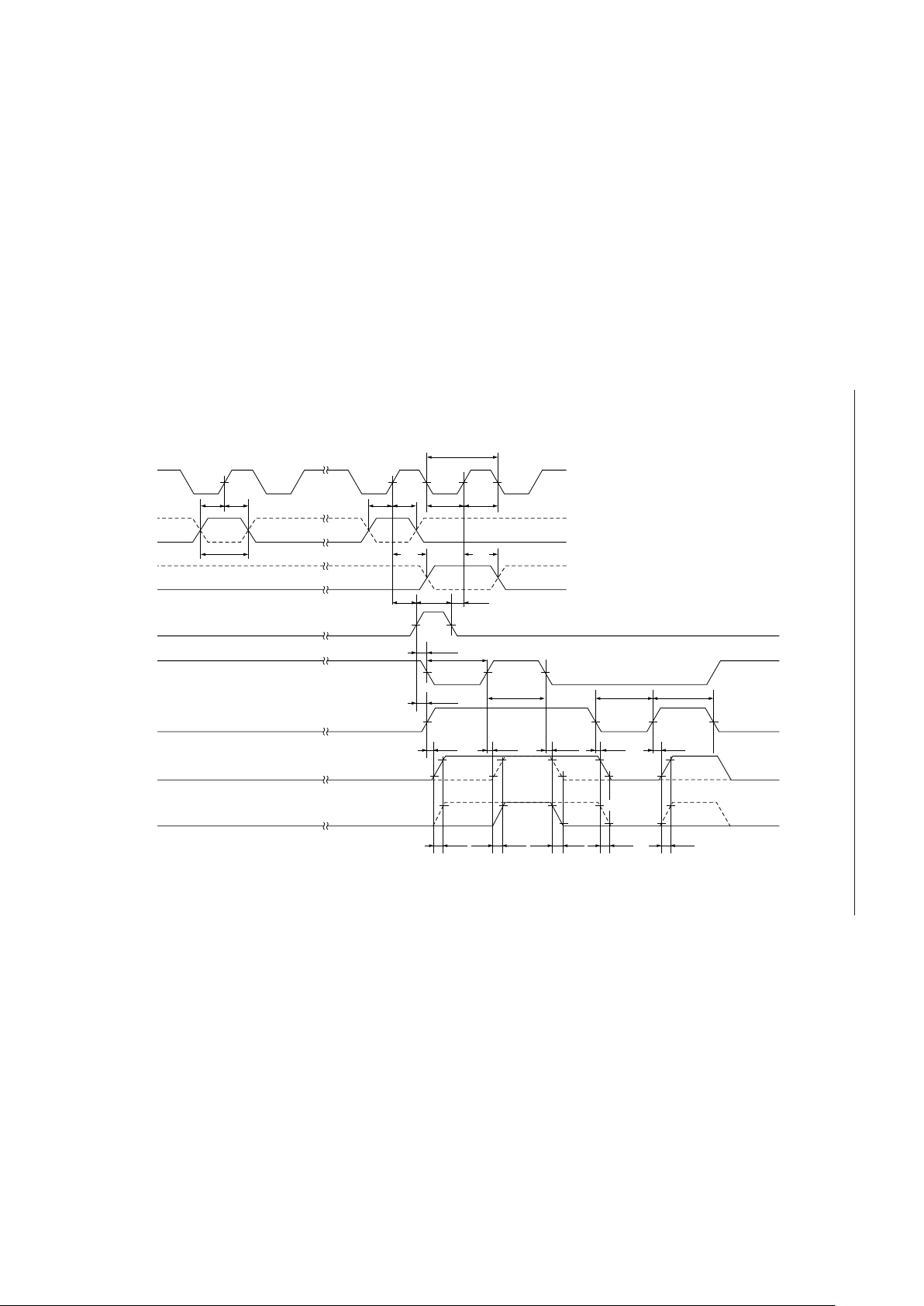
TIMING DIAGRAM
1/f f
CLOCK
DIN
LS
HVO (OTHERS)
CL
HVO (1, 2, 19, 20)
CHG
DOUT
T1/2 T3/4
T(19,20)
T1/2 T3/4
t
WCLKtWCLK
tDHt
DS
tDHt
DS
t
WD
t
PD
t
PD
t
DCLtWLStDLC
t
DLCG
t
WCHG
t
WCHG
t
DLCL
t
WCL
t
WCL
t
DLH
t
DLH
t
DHL
t
DHL
t
DLH
90%
10%
10%
t
TLH
t
TLH
t
THL
t
THL
t
TLH
90%
Page 10
¡ Semiconductor MSC1164
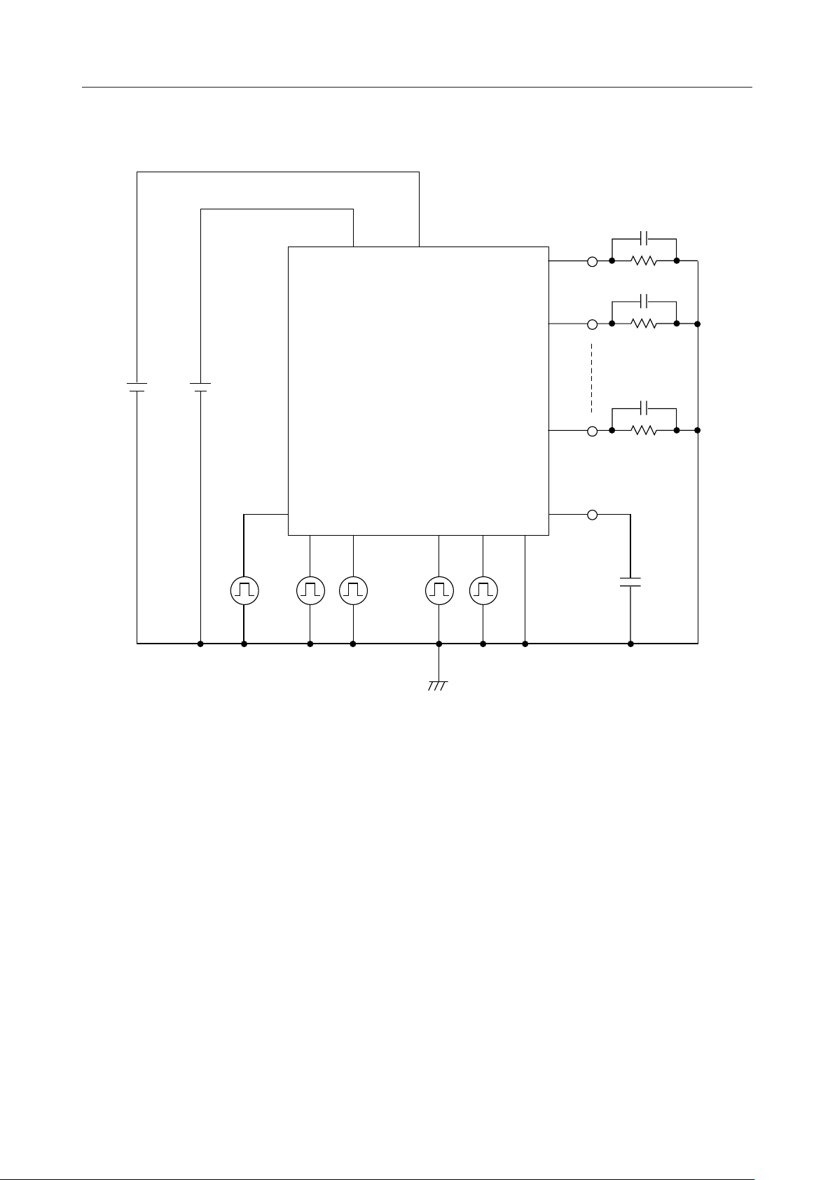
Test circuit
20pF
65V 5.0V
DIN
CLK
V
CC
V
HV
HVO1
1.5kW
HVO2
HVO20
DOUT
LS
CHG
CL
GND
30pF
10/13
Page 11
¡ Semiconductor MSC1164
FUNCTIONAL DESCRIPTION
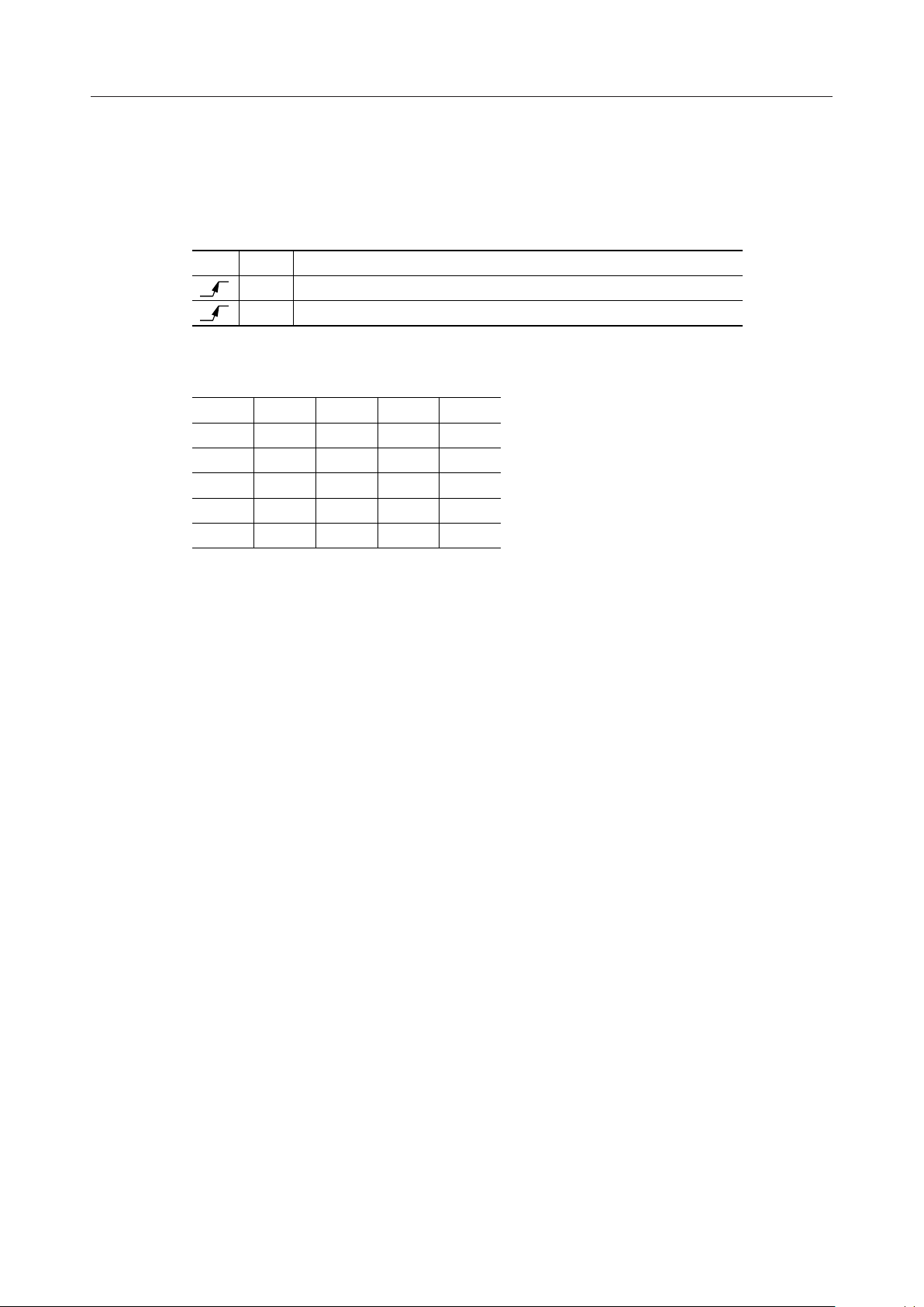
Function Table
CLK
H
L
CL CHG
L
H
H
H
L: Low Level, H: High Level, X: Don't Care, NC: Change
R-1DIN
H
R1n
L
R1n
LS
X
H
L
L
LL NCXH
X
X
H
H
R2n
R2n
R.X HVO.X
X
X
H
L
R-4R-3R-2
R3n
R3n
L
H
H
L
•••••••••••••••
R19n
R19n
DOUTR-20
R19n
R19n
NOTES ON USE
1. The MSC1164 is designed as a grid/anode driver of VFD.
The data applied to the data input pin is read into the shift register at the rising edge of the
clock and shifted sequencially to the shift register synchronizing with the clock.
The shift register output drives the output driver, passing through the latch and the NOR
circuit.
Setting the CL pin to "L" makes all driver outputs go into "L". This function can be used for
setting display blanking.
2. The contents of the shift register are undefined after power is turned on.
Therefore, two or more driver outputs may go into "H" at the same time after power-on. (If
it happens, an overloading beyond the power dissipation limit may occur to cause a device
break-down.)
To avoid this, take the following procedure:
1) Turn on the power of the logic portion while holding the CL pin to "L".
2) Turn on the power of the driver portion.
3) Apply a "L" level signal to the DIN pin and send clock pulses by the specified number
of grids to reset ("L") the entire contents of the shift register.
4) Initialize the driver outputs to "L".
11/13
Page 12
¡ Semiconductor MSC1164
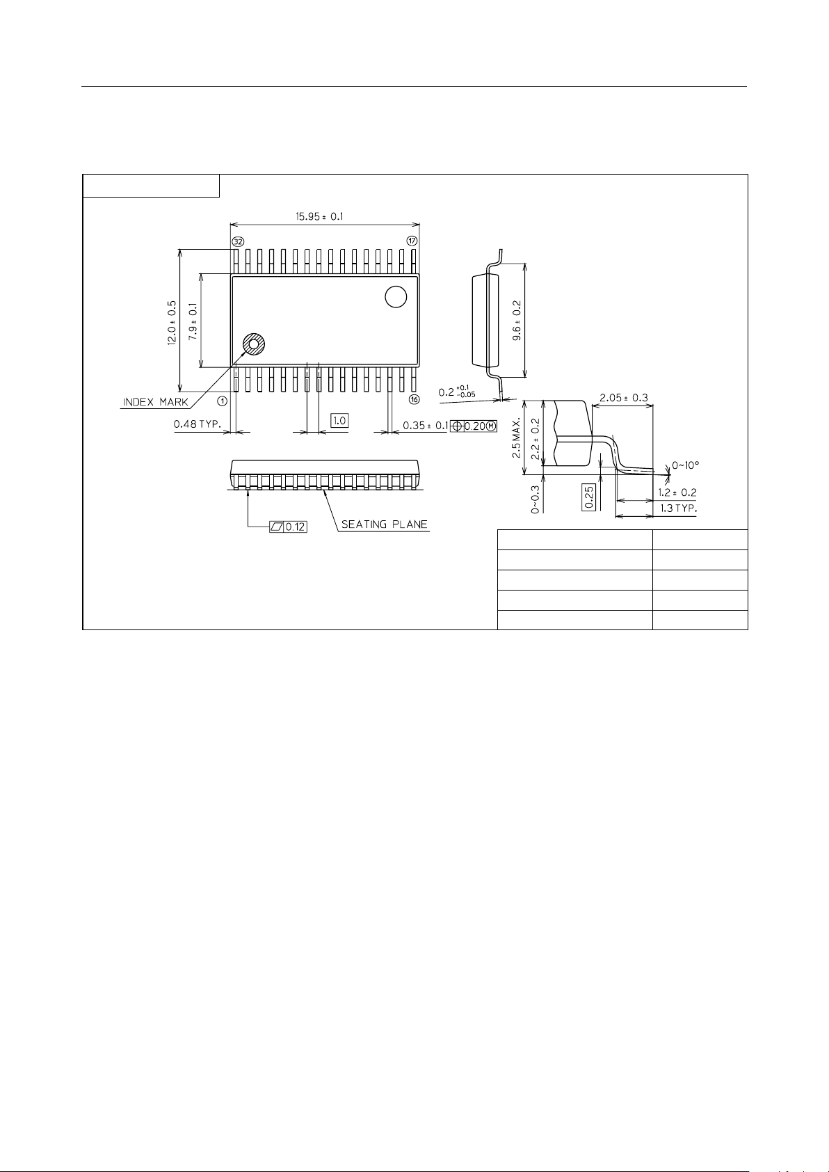
PACKAGE DIMENSIONS
(Unit : mm)
SSOP32-P-430-1.00-K
Mirror finish
Package material
Lead frame material
Pin treatment
Solder plate thickness
Package weight (g)
Epoxy resin
42 alloy
Solder plating
5 mm or more
0.60 TYP.
Notes for Mounting the Surface Mount Type Package
The SOP, QFP, TSOP, SOJ, QFJ (PLCC), SHP and BGA are surface mount type packages, which
are very susceptible to heat in reflow mounting and humidity absorbed in storage.
Therefore, before you perform reflow mounting, contact Oki’s responsible sales person for the
product name, package name, pin number, package code and desired mounting conditions
(reflow method, temperature and times).
12/13
Page 13
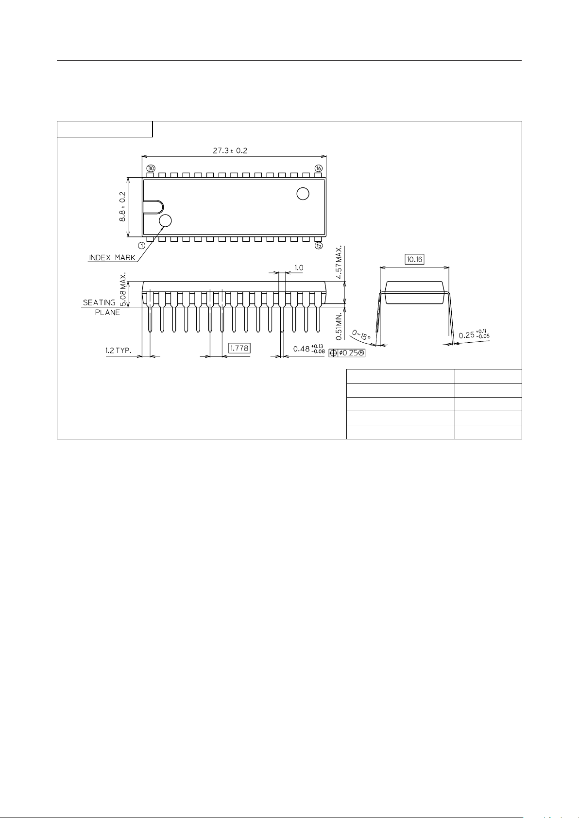
¡ Semiconductor MSC1164
(Unit : mm)
SDIP30-P-400-1.78
Package material
Lead frame material
Pin treatment
Solder plate thickness
Package weight (g)
Epoxy resin
42 alloy
Solder plating
5 mm or more
1.80 TYP.
Notes for Mounting the Surface Mount Type Package
The SOP, QFP, TSOP, SOJ, QFJ (PLCC), SHP and BGA are surface mount type packages, which
are very susceptible to heat in reflow mounting and humidity absorbed in storage.
Therefore, before you perform reflow mounting, contact Oki’s responsible sales person for the
product name, package name, pin number, package code and desired mounting conditions
(reflow method, temperature and times).
13/13
 Loading...