

Page 1

2–1
MRW3001 MRW3003 MRW3005MOTOROLA RF DEVICE DATA
The RF Line
. . . designed primarily for large–signal output and driver amplifier stages in the
1.5 to 3.0 GHz frequency range.
• Designed for Class B or C, Common Base Linear Power Amplifiers
• Specified 28 Volt, 3.0 GHz Characteristics:
Output Power — 1.0 to 5.0 Watts
Power Gain — 5.0 to 7.0 dB Min
Collector Efficiency — 30% Min
• Gold Metallization for Improved Reliability
• Diffused Ballast Resistors
• Circuit board photomaster available upon request by contacting
RF Tactical Marketing in Phoenix, AZ.
MAXIMUM RATINGS
Rating Symbol 3001 3003 3005 Unit
Collector–Base Voltage V
CBO
45 Vdc
Emitter–Base Voltage V
EBO
3.5 Vdc
Operating Junction Temperature T
J
200 °C
Storage Temperature Range T
stg
–65 to +200 °C
THERMAL CHARACTERISTICS
Characteristic Symbol Max Unit
Thermal Resistance, RF,
Junction to Case
R
θJC
35 17 8.5 °C/W
ELECTRICAL CHARACTERISTICS (T
C
= 25°C unless otherwise noted.)
Characteristic
Symbol Min Typ Max Unit
OFF CHARACTERISTICS
Collector–Emitter Breakdown Voltage
(IC = 10 mA, VBE = 0) MRW3001
(IC = 30 mA, VBE = 0) MRW3003
(IC = 50 mA, VBE = 0) MRW3005
V
(BR)CES
50
50
50
—
—
—
—
—
—
Vdc
Collector–Base Breakdown Voltage
(IC = 1.0 mA, IE = 0) MRW3001
(IC = 3.0 mA, IE = 0) MRW3003
(IC = 5.0 mA, IE = 0) MRW3005
V
(BR)CBO
45
45
45
—
—
—
—
—
—
Vdc
Emitter–Base Breakdown Voltage
(IE = 1.0 mA, IC = 0)
V
(BR)EBO
3.5 — — Vdc
Collector Cutoff Current MRW3001
(VCB = 28 V, IE = 0) MRW3003
MRW3005
I
CBO
—
—
—
—
—
—
0.5
0.75
1.25
mAdc
ON CHARACTERISTICS
DC Current Gain
(IC = 100 mA, VCE = 5.0 V) MRW3001
(IC = 300 mA, VCE = 5.0 V) MRW3003
(IC = 500 mA, VCE = 5.0 V) MRW3005
h
FE
10
10
10
—
—
—
120
120
120
—
(continued)
Order this document
by MRW3001/D
SEMICONDUCTOR TECHNICAL DATA
5.0–7.0 dB
1.5–3.0 GHz
1.0–5.0 WATTS
MICROWAVE
POWER TRANSISTORS
CASE 328A–03, STYLE 1
(GP–13)
MRW3001, 3003, 3005
Motorola, Inc. 1994
Motorola, Inc. 1994
REV 6
Page 2
MRW3001 MRW3003 MRW3005
2–2
MOTOROLA RF DEVICE DATA
ELECTRICAL CHARACTERISTICS — continued (T
C
= 25°C unless otherwise noted.)
Characteristic
Symbol Min Typ Max Unit
DYNAMIC CHARACTERISTICS
Output Capacitance MRW3001
(VCB = 28 V, IE = 0, f = 1.0 MHz) MRW3003
MRW3005
C
ob
—
—
—
3.5
5.7
8.4
4.0
7.0
10
pF
FUNCTIONAL TESTS
Common–Base Amplifier Power Gain
(VCE = 28 V, P
out
= 1.0 W, f = 3.0 GHz) MRW3001
(VCE = 28 V, P
out
= 3.0 W, f = 3.0 GHz) MRW3003
(VCE = 28 V, P
out
= 5.0 W, f = 3.0 GHz) MRW3005
G
PB
7.0
6.0
5.0
—
—
—
—
—
—
dB
Collector Efficiency
(VCE = 28 V, P
out
= 1.0 W, f = 3.0 GHz) MRW3001
(VCE = 28 V, P
out
= 3.0 W, f = 3.0 GHz) MRW3003
(VCE = 28 V, P
out
= 5.0 W, f = 3.0 GHz) MRW3005
η
c
30
30
30
—
—
—
—
—
—
%
Load Mismatch
(VCE = 28 V, f = 3.0 GHz, Load VSWR = ∞:1, All Phase Angles)
P
out
= 1.0 W MRW3001
P
out
= 3.0 W MRW3003
P
out
= 5.0 W MRW3005
ψ
No Degradation in Output Power
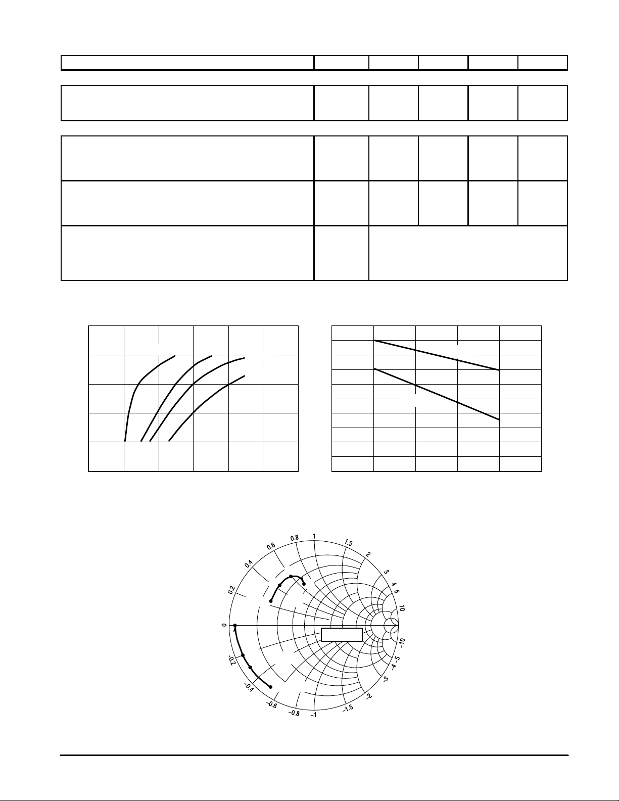
Figure 1. Output Power versus Input Power
MRW3001
TYPICAL CHARACTERISTICS
P , OUTPUT POWER (WATTS)
out
2.5
2
1.5
1
0.5
0
Pin, INPUT POWER (WATTS)
0 0.05 0.1 0.15 0.2 0.25 0.3
2 GHz
3 GHz
f = 1.5 GHz
2.3 GHz
2.5
2
1.5
1
0.5
0
1
f, FREQUENCY (GHz)
1.5 2 2.5 3 3.5
60
50
40
30
20
c
η
, EFFICIENCY (%)
P
sat
, SATURATED OUTPUT POWER (WATTS)
η
c
@ 1 W
P
o(sat)
0.4 0.6 0.8 1.0 1.5
2 3 4 5
100.2
3
2.3
2
f = 1.5 GHz
3
2.3
2
f = 1.5 GHz
Zo = 50
Ω
ZOL*
Z
in
Figure 2. P
sat
and η versus Frequency
Figure 3. Series Equivalent Input/Output Impedance
Page 3

2–3
MRW3001 MRW3003 MRW3005MOTOROLA RF DEVICE DATA
MRW3003
TYPICAL CHARACTERISTICS
P , OUTPUT POWER (WATTS)
out
5
4
3
2
1
0
Pin, INPUT POWER (WATTS)
0 0.1
2 GHz
3 GHz
f = 1.5 GHz
2.3 GHz
0.2 0.3 0.4 0.5 0.6
8
1
f, FREQUENCY (GHz)
1.5 2 2.5 3 3.5
80
60
40
20
c
η
, EFFICIENCY (%)
η
c
@ 3 W
P
o(sat)
6
4
2
0
3
2.3
2
f = 1.5 GHz
2.3
0.4 0.6 0.8 1.0 1.5
2 3 4 5
100.2
2
f = 1.5 GHz
3
P
in
, INPUT POWER (WATTS)
Zo = 50
Ω
ZOL*
Z
in
Figure 4. Output Power versus Input Power Figure 5. P
sat
and η versus Frequency
Figure 6. Series Equivalent Input/Output Impedance
Page 4

MRW3001 MRW3003 MRW3005
2–4
MOTOROLA RF DEVICE DATA
MRW3005
TYPICAL CHARACTERISTICS
P , OUTPUT POWER (WATTS)
out
10
8
6
4
2
0
0.2
2 GHz
1.5 GHz
0.6 1 1.4 1.8 2.2 2.6
f = 3 GHz
2.3 GHz
14
1
f, FREQUENCY (GHz)
1.5 2 2.5 3 3.5
60
40
20
c
η
, EFFICIENCY (%)
η
c
@ 5 W
P
o(sat)
12
10
8
6
4
3
2.3
f = 1.5 GHz
2
3
2.3
0.4 0.6 0.8 1.0 1.5
2 3 4 5
100.2
2
f = 1.5 GHz
Zo = 50
Ω
ZOL*
Z
in
P
in
, INPUT POWER (WATTS)
P
sat
, SATURATED OUTPUT POWER (WATTS)
Figure 7. Output Power versus Input Power Figure 8. P
sat
and η versus Frequency
Figure 9. Series Equivalent Input/Output Impedance
The graph shown displays MTTF in hours x ampere2 emitter current
for each of the 3.0 GHz devices. Life tests at elevated temperatures
have correlated to better than ±10% to the theoretical prediction for
metal failure. CAUTION — A calculation is required to obtain actual
metal life. Sample MTTF calculations based on operating conditions
are shown below.
Junction Temperature — °C
To calculate metal lifetime under any set of conditions, obtain actual
data or estimate from typical performance curves. Solve for TJ (°C):
P
out
x 100
hc%
(1) TJ = θ
JF
MTTF Factor
(Normalized to 1.0 ampere2 Continuous Duty)
+ Pin – P
out
+ T
FLANGE
Enter graph of MTF factor versus TJ. Obtain MTF factor. Calculate
metal life by:
(2) Metal Life in Hours =
MTF Factor
I
C
2 (Amps)
MTTF FACTOR (HRS x AMP
2
)
10,000,000
1,000,000
100,000
10,000
1,000
100
23021019017015013011090
TJ, JUNCTION TEMPERATURE (
°
C)
MRW3005
MRW3003
MRW3001
Figure 10. MTTF Factor versus
Junction Temperature
Page 5

2–5
MRW3001 MRW3003 MRW3005MOTOROLA RF DEVICE DATA
PACKAGE DIMENSIONS
CASE 328A–03
ISSUE D
NOTES:
1. DIMENSIONING AND TOLERANCING PER ANSI
Y14.5M. 1982.
2. CONTROLLING DIMENSION: INCH.
F
R
E
1 2
DIM MIN MAX MIN MAX
MILLIMETERSINCHES
A 0.795 0.805 20.20 20.45
B 0.245 0.255 6.23 6.47
C 0.145 0.170 3.69 4.31
D 0.115 0.125 2.93 3.17
E 0.055 0.065 1.40 1.65
F 0.045 0.055 1.15 1.39
G 0.562 BSC 14.27 BSC
J 0.003 0.006 0.08 0.15
K 0.260 0.375 6.60 9.52
N 0.175 0.185 4.45 4.69
Q 0.120 0.135 3.05 3.42
R 0.225 0.235 5.72 5.97
S 0.120 0.130 3.05 3.30
3
G D
Q
2 PL
–B–
–A–
M
A
M
0.15 (0.006) B
M
T
J
S
C
K K
N
SEATING
–T–
PLANE
STYLE 1:
PIN 1. EMITTER
2. COLLECTOR
3. BASE
Page 6

MRW3001 MRW3003 MRW3005
2–6
MOTOROLA RF DEVICE DATA
Motorola reserves the right to make changes without further notice to any products herein. Motorola makes no warranty , representation or guarantee regarding
the suitability of its products for any particular purpose, nor does Motorola assume any liability arising out of the application or use of any product or circuit,
and specifically disclaims any and all liability, including without limitation consequential or incidental damages. “T ypical” parameters can and do vary in different
applications. All operating parameters, including “T ypicals” must be validated for each customer application by customer’s technical experts. Motorola does
not convey any license under its patent rights nor the rights of others. Motorola products are not designed, intended, or authorized for use as components in
systems intended for surgical implant into the body, or other applications intended to support or sustain life, or for any other application in which the failure of
the Motorola product could create a situation where personal injury or death may occur. Should Buyer purchase or use Motorola products for any such
unintended or unauthorized application, Buyer shall indemnify and hold Motorola and its officers, employees, subsidiaries, affiliates, and distributors harmless
against all claims, costs, damages, and expenses, and reasonable attorney fees arising out of, directly or indirectly, any claim of personal injury or death
associated with such unintended or unauthorized use, even if such claim alleges that Motorola was negligent regarding the design or manufacture of the part.
Motorola and are registered trademarks of Motorola, Inc. Motorola, Inc. is an Equal Opportunity/Affirmative Action Employer.
Literature Distribution Centers:
USA: Motorola Literature Distribution; P.O. Box 20912; Phoenix, Arizona 85036.
EUROPE: Motorola Ltd.; European Literature Centre; 88 T anners Drive, Blakelands, Milton Keynes, MK14 5BP, England.
JAPAN: Nippon Motorola Ltd.; 4-32-1, Nishi-Gotanda, Shinagawa-ku, Tokyo 141, Japan.
ASIA PACIFIC: Motorola Semiconductors H.K. Ltd.; Silicon Harbour Center, No. 2 Dai King Street, Tai Po Industrial Estate, Tai Po, N.T., Hong Kong.
MRW3001/D
*MRW3001/D*
◊
 Loading...