

Page 1
SEMICONDUCTOR TECHNICAL DATA
The RF Line
Order this document
by MRW2001/D
Designed primarily for large–signal output and driver amplifier stages in the
1.0 to 2.3 GHz frequency range.
• Designed for Class B or C, Common Base Power Amplifiers
• Specified 28 Volt, 2.0 GHz Characteristics:
Output Power — 1.0 to 20 Watts
Power Gain — 5.2 to 9.0 dB, Min
Collector Efficiency — 40%, Min
• Gold Metallization for Improved Reliability
• Diffused Ballast Resistors
• Circuit board photomaster available upon request by contacting
RF Tactical Marketing in Phoenix, AZ.
5.2–9.0 dB
1.0–2.3 GHz
1.0 – 20 W
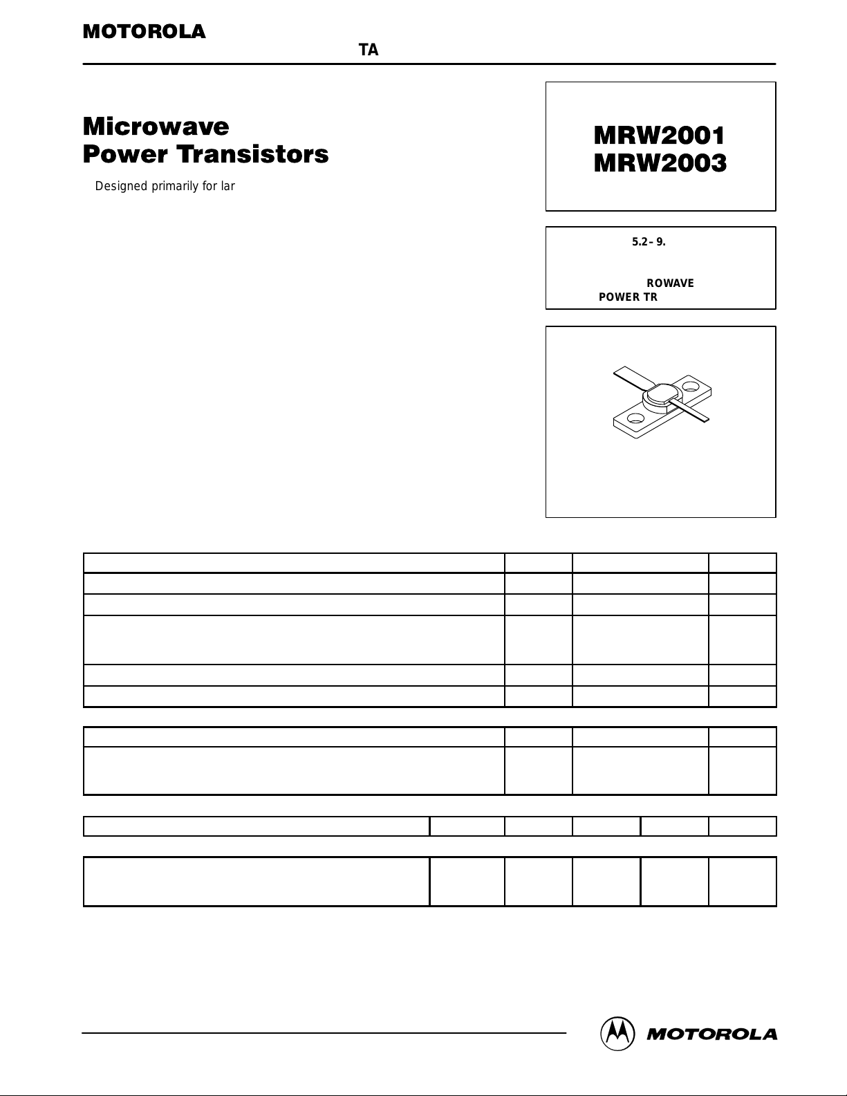
MICROWAVE
POWER TRANSISTORS
CASE 328A–03, STYLE 1
(GP–13)
MAXIMUM RATINGS
Rating Symbol Value Unit
Collector–Base Voltage V
Emitter–Base Voltage V
Collector Current — Continuous
Operating Junction Temperature T
Storage Temperature Range T
MRW2001
MRW2003
THERMAL CHARACTERISTICS
Characteristic Symbol Max Unit
Thermal Resistance, RF, Junction to Case
ELECTRICAL CHARACTERISTICS (T
Characteristic
= 25°C unless otherwise noted)
C
MRW2001
MRW2003
Symbol Min Typ Max Unit
OFF CHARACTERISTICS
Collector–Emitter Breakdown V oltage
(IC = 10 mA, VBE = 0) MRW2001
(IC = 20 mA, VBE = 0) MRW2003
V
(BR)CES
CES
EBO
R
I
C
J
stg
θJC
50
50
50 Vdc
3.5 Vdc
0.25
0.5
200 °C
–65 to +200 °C
25
15
—
—
—
—
(continued)
Adc
°C/W
Vdc
REV 8
Motorola, Inc. 1997
MRW2001 MRW2003MOTOROLA RF DEVICE DATA
1
Page 2
ELECTRICAL CHARACTERISTICS — continued (T
Characteristic Symbol Min Typ Max Unit
= 25°C unless otherwise noted)
C
OFF CHARACTERISTICS (continued)
Emitter–Base Breakdown Voltage
(IE = 0.2 mA, IC = 0) MRW2001
(IE = 0.25 mA, IC = 0) MRW2003
Collector Cutoff Current MRW2001
(VCB = 28 V, IE = 0) MRW2003
ON CHARACTERISTICS
DC Current Gain
(IC = 100 mA, VCE = 5.0 V) MRW2001
(IC = 100 mA, VCE = 5.0 V) MRW2003
DYNAMIC CHARACTERISTICS
Output Capacitance MRW2001
(VCB = 28 V, IE = 0, f = 1.0 MHz) MRW2003
FUNCTIONAL TESTS
Common–Base Amplifier Power Gain
(VCE = 28 V, P
Common–Base Amplifier Power Gain
(VCE = 28 V, P
Collector Efficiency
(VCE = 28 V, P
(VCE = 28 V, P
Load Mismatch
(VCE = 28 V, f = 2.0 GHz, Load VSWR = ∞:1, All Phase Angles)
P
= 1.0 W MRW2001
out
P
= 3.0 W MRW2003
out
Saturated Output Power
(VCE = 28 V, f = 2.3 GHz) MRW2001
(VCE = 28 V, f = 1.5 GHz)
(VCE = 28 V, f = 1.0 GHz)
(VCE = 28 V, f = 2.3 GHz) MRW2003
(VCE = 28 V, f = 1.5 GHz)
(VCE = 28 V, f = 1.0 GHz)
= 1.0 W, f = 2.0 GHz) MRW2001
out
= 3.0 W, f = 2.0 GHz) MRW2003
out
= 1.0 W, f = 2.0 GHz) MRW2001
out
= 3.0 W, f = 2.0 GHz) MRW2003
out
V
(BR)EBO
I
CBO
h
FE
C
ob
G
PB
G
PB
η 40 — — %
ψ
P
sat1
P
sat2
P
sat3
3.5
3.5
—
—
10
10
—
—
9.0 — — dB
8.0 — — dB
—
—
—
—
—
—
—
—
—
—
—
—
—
—
No Degradation in Output Power
1.0
1.2
1.3
3.0
3.7
4.0
—
—
0.5
0.5
120
100
4.0
5.0
—
—
—
—
—
—
Vdc
mAdc
—
pF
W
MRW2001 MRW2003
2
MOTOROLA RF DEVICE DATA
Page 3

TYPICAL CHARACTERISTICS
3
2
1
0
MRW2001 MRW2003
f = 1 GHz
Pin, POWER INPUT (WATTS)
1.5 GHz
2 GHz
2.3 GHz
VCC = 28 V
0.30.20.10
6
5
4
3
2
out
P , POWER OUTPUT (WATTS)
1
0
1000
Pin, POWER INPUT (WATTS)
f = 1 GHz
200 300 400 500
1.5 GHz
2 GHz
2.3 GHz
VCC = 28 V
Figure 1. Output Power versus Input Power
MRW2001 MRW2003
1.5
1
f = 2.3 GHz
2
ZOL*
0.2 0.4 0.6 0.8 1 2 3 5 101.5 4
f = 1 GHz
1.5
Z
in
2.3
2
1.5
2
2.3
f = 1 GHz
ZOL*
f = 1 GHz
0.2 0.4 0.6 0.8 1 2 3 5 101.5 4
Zo = 50
1.5
Z
2
in
2.3
Ω
70
60
50
40
30
Zo = 50
Ω
Figure 2. Series Equivalent Input/Output Impedance
VCC = 28 V
MRW2001 MRW2003
2.5
P
o
η
c
VCC = 28 V
13
1.5 2 2.5
f, FREQUENCY (GHz)
2
1.5
1
0.5
, SATURATED OUTPUT POWER (WATTS)
sat
P
80
70
60
, EFFICIENCY (%)
c
η
50
40
η
c
P
o(sat)
VCC = 28 V
13
1.5 2 2.5
f, FREQUENCY (GHz)
6
5
4
3
Figure 3. Power Output and Efficiency versus Frequency
MRW2001 MRW2003MOTOROLA RF DEVICE DATA
3
Page 4

The graph shown below displays MTTF in hours x ampere
emitter current for each of the “Super 2.0 GHz” devices. Life
tests at elevated temperatures have correlated to better than
±10% to the theoretical prediction for metal failure. Sample
MTTF calculations based on operating conditions are included on the graph.
100
)
2
10
1
HRS. X AMP
6
0.1
MRW2003
2
0.01
MTTF FACTOR (10
0.001
70 90 110 130 150 170 190 210
C
B
fo
t
50
Ω
C
C
x
MRW2001
2.0 GHz
Board Material = 0.062″ Glass-Teflon εr = 2.55
MRW2001
TJ, JUNCTION TEMPERATURE (
Figure 4. MTTF Factor
50
Ω
C
C
Figure 5. PC Board Layouts
°
C)
C
fo
50
Ω
RFC
MRW2003
2.0 GHz
Board Material = 0.020″ Glass-Teflon εr = 2.55
C
x
50
Ω
C
C
MRW2001 MRW2003
4
MOTOROLA RF DEVICE DATA
Page 5

–A–
GD
C
S
P ACKAGE DIMENSIONS
–B–
2 PL
Q
0.15 (0.006) B
12
3
K
N
F
K
M
R
J
M
A
T
NOTES:
M
1. DIMENSIONING AND TOLERANCING PER ANSI
Y14.5M. 1982.
2. CONTROLLING DIMENSION: INCH.
E
STYLE 1:
SEATING
–T–
PLANE
CASE 328A–03
ISSUE E
DIM MIN MAX MIN MAX
A 0.795 0.805 20.20 20.45
B 0.245 0.255 6.23 6.47
C 0.145 0.170 3.69 4.31
D 0.115 0.125 2.93 3.17
E 0.055 0.065 1.40 1.65
F 0.045 0.055 1.15 1.39
G 0.562 BSC 14.27 BSC
J 0.003 0.006 0.08 0.15
K 0.260 0.375 6.60 9.52
N 0.175 0.185 4.45 4.69
Q 0.120 0.135 3.05 3.42
R 0.225 0.235 5.72 5.97
S 0.120 0.130 3.05 3.30
1. EMITTER
2. COLLECTOR
3. BASE
MILLIMETERSINCHES
MRW2001 MRW2003MOTOROLA RF DEVICE DATA
5
Page 6

Motorola reserves the right to make changes without further notice to any products herein. Motorola makes no warranty , representation or guarantee regarding
the suitability of its products for any particular purpose, nor does Motorola assume any liability arising out of the application or use of any product or circuit, and
specifically disclaims any and all liability, including without limitation consequential or incidental damages. “T ypical” parameters which may be provided in Motorola
data sheets and/or specifications can and do vary in different applications and actual performance may vary over time. All operating parameters, including “Typicals”
must be validated for each customer application by customer’s technical experts. Motorola does not convey any license under its patent rights nor the rights of
others. Motorola products are not designed, intended, or authorized for use as components in systems intended for surgical implant into the body, or other
applications intended to support or sustain life, or for any other application in which the failure of the Motorola product could create a situation where personal injury
or death may occur. Should Buyer purchase or use Motorola products for any such unintended or unauthorized application, Buyer shall indemnify and hold Motorola
and its officers, employees, subsidiaries, affiliates, and distributors harmless against all claims, costs, damages, and expenses, and reasonable attorney fees
arising out of, directly or indirectly, any claim of personal injury or death associated with such unintended or unauthorized use, even if such claim alleges that
Motorola was negligent regarding the design or manufacture of the part. Motorola and are registered trademarks of Motorola, Inc. Motorola, Inc. is an Equal
Opportunity/Affirmative Action Employer.
How to reach us:
USA/EUROPE/Locations Not Listed: Motorola Literature Distribution; JAPAN: Nippon Motorola Ltd.: SPD, Strategic Planning Office, 4–32–1,
P.O. Box 5405, Denver, Colorado 80217. 303–675–2140 or 1–800–441–2447 Nishi–Gotanda, Shinagawa–ku, T o kyo 141, Japan. 81–3–5487–8488
Mfax: RMFAX0@email.sps.mot.com – TOUCHTONE 602–244–6609 ASIA/PACIFIC: Motorola Semiconductors H.K. Ltd.; 8B Tai Ping Industrial Park,
– US & Canada ONLY 1–800–774–1848 51 Ting Kok Road, T ai Po, N.T., Hong Kong. 852–26629298
INTERNET: http://motorola.com/sps
Mfax is a trademark of Motorola, Inc.
MRW2001 MRW2003
6
◊
MOTOROLA RF DEVICE DATA
MRW2001/D
 Loading...