

Page 1
SEMICONDUCTOR TECHNICAL DATA
The MRFIC Line
The MRFIC2404 is a single–stage class A GaAs amplifier in a low–cost
8 lead plastic package designed to drive the MRFIC2403 power amplifier for
use in the 2.4 to 2.5 GHz Industrial–Scientific–Medical (ISM) band. The design
is optimized for 5.0 Volt operation at 2.45 GHz but is usable from 2.0 to 3.0 GHz
in applications such as telemetry and Multichannel Multipoint Distribution
System (MMDS) wireless cable TV systems. Performance is suitable for
frequency hopping or direct sequence spread spectrum as well as single–frequency applications.
• High Output Capability = +5.0 dBm Typical
• High Gain = 17 dB Typical
• Low Current Drain = 9.0 mA Typical
• Single Supply Voltage = 5.0 Volts
• Good Noise Figure = 4.3 dB Typical
• Low–Cost, Low Profile Plastic SOIC Package
• Order MRFIC2404R2 for Tape and Reel.
R2 Suffix = 2,500 Units per 12 mm, 13 inch Reel.
• Device Marking = M2404
Order this document
by MRFIC2404/D
2.4 GHz
EXCITER AMPLIFIER
GaAs MONOLITHIC
INTEGRATED CIRCUIT
CASE 751-05
(SO-8)
ABSOLUTE MAXIMUM RATINGS
Supply Voltage V
RF Input Power RF IN +10 dBm
Bias Enable Voltage V
Ambient Operating Temperature T
Storage Temperature T
(TA = 25_C unless otherwise noted)
Parameter Symbol Value Unit
12 Vdc
6.0 Vdc
–30 to +85
–65 to +125
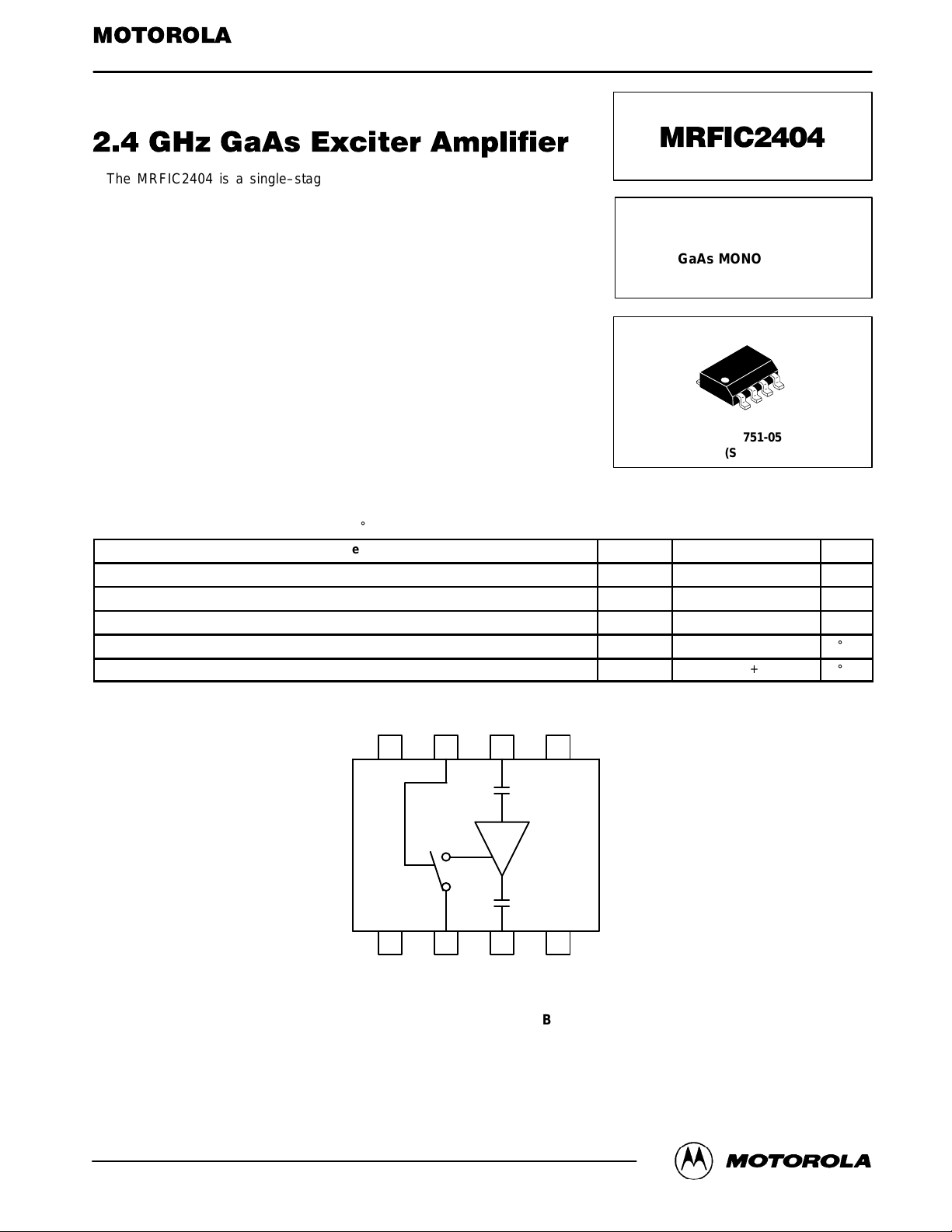
GND GND
8
1
GND GND
BIAS
DD
RF INV
7 6 5
2 3 4
RF OUTV
DD
bias
A
stg
_
C
_
C
REV 2
Motorola, Inc. 1995
Pin Connections and Functional Block Diagram
MRFIC2404MOTOROLA RF DEVICE DATA
1
Page 2
RECOMMENDED OPERATING CONDITIONS
Parameter Symbol Value Unit
Supply Voltage V
Bias Enable Voltage – ON V
Bias Enable Voltage – OFF V
Operating Frequency Range f
DD
bias
bias
OP
4.75 to 5.25 Vdc
0 Vdc
5.0 Vdc
2000 to 3000 MHz
ELECTRICAL CHARACTERISTICS (V
Characteristic Min Typ Max Unit
Small Signal Gain 16 17 – dB
Power Output, 1.0 dB Compression – +5.0 – dBm
Power Output (Pin = –11 dBm) 4.0 5.0 – dBm
Third Order Intercept Point – +15 – dBm
Noise Figure – 4.3 – dB
Reverse Isolation – 25 – dB
Turn On Time – 1.0 –
Supply Current – 9.0 12 mA
SLEEP Mode Supply Current (V
= 5.0 Vdc) – 800 –
bias
RF IN
V
BIAS
= 5.0 Vdc, TA= 25_C, RF = 2.45 GHz, V
DD
5
6
7
8
4
3
2
1
bias
T1
= 0 Vdc)
C1
V
DD
RF OUT
m
s
m
A
C1 – 15 pF
T1 – 100 W Line, 185 MILs (3.3 nH)
Board Material – 30 MIL FR4
Connectors – SMA Type
Figure 1. Applications Circuit Configuration
MRFIC2404
2
MOTOROLA RF DEVICE DATA
Page 3

T able 1. Scattering Parameters
(VDD = 5 V, TA = 25°C, 50 W System)
f
(MHz) |S11| ∠ φ |S21| ∠ φ |S12| ∠ φ |S22| ∠ φ
2000 0.232 –92.34 6.290 165.97 0.024 –51.08 0.483 –123.13
2050 0.174 –90.78 7.049 147.75 0.029 –66.26 0.383 –125.77
2100 0.122 –76.88 7.563 127.95 0.032 –78.38 0.281 –124.34
2150 0.102 –48.38 7.803 109.02 0.035 –97.84 0.191 –109.23
2200 0.128 –19.45 8.046 91.04 0.037 –105.62 0.159 –80.33
2250 0.185 –6.60 8.144 72.36 0.039 –123.88 0.196 –53.35
2300 0.244 –5.52 7.977 55.31 0.038 –135.36 0.273 –42.38
2350 0.300 –8.04 7.979 39.91 0.043 –144.83 0.350 –41.15
2400 0.343 –12.42 8.147 23.40 0.044 –160.94 0.423 –43.39
2450 0.379 –17.11 8.020 5.27 0.045 –173.09 0.477 –47.05
2500 0.403 –21.90 7.550 –10.93 0.041 173.83 0.522 –50.67
2550 0.424 –26.32 7.245 –25.36 0.043 165.85 0.556 –54.67
2600 0.436 –30.95 6.911 –39.88 0.042 154.14 0.582 –58.35
2650 0.443 –34.94 6.631 –52.32 0.041 145.35 0.600 –62.23
2700 0.447 –39.48 6.566 –65.57 0.044 135.12 0.610 –65.41
2750 0.445 –43.12 6.338 –79.97 0.043 123.72 0.622 –68.57
2800 0.446 –46.68 6.009 –93.15 0.042 114.52 0.624 –72.06
2850 0.441 –50.42 5.733 –105.10 0.043 107.18 0.620 –74.86
2900 0.439 –53.14 5.565 –116.69 0.041 98.95 0.617 –77.74
2950 0.437 –57.27 5.393 –129.54 0.042 90.72 0.608 –80.01
3000 0.409 –61.28 4.938 –142.70 0.043 81.68 0.611 –81.12
S
11
S
21
S
12
S
22
MRFIC2404MOTOROLA RF DEVICE DATA
3
Page 4

19
18
17
16
G, GAIN (dB)
15
14
13
12
2.0
Pin = – 20 dBm
VDD = 5.0 Vdc
V
= 0 Vdc
bias
25°C
85°C
2.4
f, FREQUENCY (GHz)
2.7
T ypical Characteristics
TA = – 30°C
3.0
5.0
4.8
4.6
4.4
4.2
4.0
3.8
SSB NOISE FIGURE (dB)
3.6
VDD = 5.0 Vdc
3.4
V
= 0 Vdc
bias
3.2
3.0
2.1 2.3 2.5 2.7 2.92.1 2.2 2.3 2.5 2.6 2.8 2.9
3.02.82.22.0 2.62.4
f, FREQUENCY (GHz)
Figure 2. Gain versus Frequency
8
6
4
2
0
–2
, OUTPUT POWER (dBm)
–4
out
P
–6
–8
–20
PIN, INPUT POWER (dBm)
Figure 4. Output Power versus Input Power
DESIGN AND APPLICATIONS INFORMATION
The MRFIC2404 is a single–stage GaAs amplifier
designed for exciter applications such as driving the
MRFIC2403 power amplifier. The 4.3 dB noise figure, 17 dB
gain and +5.0 dBm power output at 1.0 dB gain compression
make the MRFIC2404 suitable for high–performance
receiver IF application, Multichannel Multipoint Distribution
System (MMDS) applications, telemetry and other applications in the 2.0 to 3.0 GHz range.
The characterization curves show typical performance in
the 2.0 to 3.0 GHz range in the circuit shown in Figure 1. This
circuit was also used to derive the device impedance shown
in Table 1. The amplifier input is matched to 50 W while the
output requires about 3.3 nH series inductance for best
Figure 3. Noise Figure versus Frequency
f = 2.45 GHz
VDD = 5.0 Vdc
V
= 0 Vdc
bias
–10
–5–15–25
match at 2.45 GHz. The VDD supply line should be bypassed
as close to the chip as possible to avoid low frequency
oscillations. Power supply “stiffening” and digital transient
bypassing in the form of electrolytic of tantalum capacitors
should be added.
The device can be put into a reduced current “sleep” mode
by 5.0 Vdc to the V
bias
pin.
EVALUATION BOARDS
Evaluation boards are available for RF Monolithic Integrated Circuits by adding a “TF” suffix to the device type.
For a complete list of currently available boards and ones
in development for newly introduced product, please con tact your local Motorola Distributor or Sales Office.
MRFIC2404
4
MOTOROLA RF DEVICE DATA
Page 5

P ACKAGE DIMENSIONS
C
A
E
B
A1
D
58
0.25MB
1
H
4
e
M
h
X 45
_
q
C
A
SEATING
PLANE
0.10
L
B
SS
A0.25MCB
NOTES:
1. DIMENSIONING AND TOLERANCING PER ASME
Y14.5M, 1994.
2. DIMENSIONS ARE IN MILLIMETERS.
3. DIMENSION D AND E DO NOT INCLUDE MOLD
PROTRUSION.
4. MAXIMUM MOLD PROTRUSION 0.15 PER SIDE.
5. DIMENSION B DOES NOT INCLUDE MOLD
PROTRUSION. ALLOWABLE DAMBAR
PROTRUSION SHALL BE 0.127 TOTAL IN EXCESS
OF THE B DIMENSION AT MAXIMUM MATERIAL
CONDITION.
MILLIMETERS
DIM MIN MAX
A 1.35 1.75
A1 0.10 0.25
B 0.35 0.49
C 0.18 0.25
D 4.80 5.00
E
3.80 4.00
1.27 BSCe
H 5.80 6.20
h
0.25 0.50
L 0.40 1.25
0 7
q
__
CASE 751–05
ISSUE S
MRFIC2404MOTOROLA RF DEVICE DATA
5
Page 6

Motorola reserves the right to make changes without further notice to any products herein. Motorola makes no warranty , representation or guarantee regarding
the suitability of its products for any particular purpose, nor does Motorola assume any liability arising out of the application or use of any product or circuit, and
specifically disclaims any and all liability, including without limitation consequential or incidental damages. “T ypical” parameters which may be provided in Motorola
data sheets and/or specifications can and do vary in different applications and actual performance may vary over time. All operating parameters, including “Typicals”
must be validated for each customer application by customer’s technical experts. Motorola does not convey any license under its patent rights nor the rights of
others. Motorola products are not designed, intended, or authorized for use as components in systems intended for surgical implant into the body, or other
applications intended to support or sustain life, or for any other application in which the failure of the Motorola product could create a situation where personal injury
or death may occur. Should Buyer purchase or use Motorola products for any such unintended or unauthorized application, Buyer shall indemnify and hold Motorola
and its officers, employees, subsidiaries, affiliates, and distributors harmless against all claims, costs, damages, and expenses, and reasonable attorney fees
arising out of, directly or indirectly, any claim of personal injury or death associated with such unintended or unauthorized use, even if such claim alleges that
Motorola was negligent regarding the design or manufacture of the part. Motorola and are registered trademarks of Motorola, Inc. Motorola, Inc. is an Equal
Opportunity/Affirmative Action Employer.
How to reach us:
USA/EUROPE/Locations Not Listed: Motorola Literature Distribution; JAPAN: Nippon Motorola Ltd.: SPD, Strategic Planning Office, 4–32–1,
P.O. Box 5405, Denver, Colorado 80217. 303–675–2140 or 1–800–441–2447 Nishi–Gotanda, Shinagawa–ku, Tokyo 141, Japan. 81–3–5487–8488
Mfax: RMFAX0@email.sps.mot.com – TOUCHTONE 602–244–6609 ASIA/PACIFIC: Motorola Semiconductors H.K. Ltd.; 8B Tai Ping Industrial Park,
– US & Canada ONLY 1–800–774–1848 51 Ting Kok Road, T ai Po, N.T., Hong Kong. 852–26629298
INTERNET: http://motorola.com/sps
Mfax is a trademark of Motorola, Inc.
MRFIC2404
6
◊
MOTOROLA RF DEVICE DATA
MRFIC2404/D
*MRFIC2404/D*
 Loading...