

Page 1
SEMICONDUCTOR TECHNICAL DATA
The MRFIC Line
The MRFIC2403 is a two–stage class B GaAs power amplifier in a low–cost
16 lead plastic package designed for use in the 2.4 to 2.5 GHz Industrial–
Scientific–Medical (ISM) band. The design is optimized for efficiency at 5.0 V olt
operation at 2.5 GHz but is usable from 2.0 to 3.0 GHz in applications such as
telemetry and Multichannel Multipoint Distribution System (MMDS) wireless
cable TV systems. Performance is suitable for frequency hopping or direct
sequence spread spectrum as well as single–frequency applications. Power
control circuitry allows 20 dB dynamic range for setting the output power.
• High Output Power = +23.5 dBm Typical
• High Gain = 23 dB Typical
• Excellent Efficiency = 55% Typical
• Power Control = 20 dB Range
• Low–Cost, Low Profile Plastic SOIC Package
• Available in Tape and Reel by Adding R2 Suffix to Part Number.
R2 Suffix = 2,500 Units per 16 mm, 13 inch Reel.
• Device Marking = M2403
Order this document
by MRFIC2403/D
2.4 GHz
POWER AMPLIFIER
GaAs MONOLITHIC
INTEGRATED CIRCUIT
CASE 751B-05
(SO–16)
ABSOLUTE MAXIMUM RATINGS
Supply Voltage V
Power Control Voltage V
Gate Bias Voltage VG1, V
RF Input Power RF IN +10 dBm
Ambient Operating Temperature T
Storage Temperature T
(TA = 25_C unless otherwise noted)
Parameter Symbol Value Unit
6.0 Vdc
6.0 Vdc
–4.0 Vdc
–30 to +85
–65 to +125
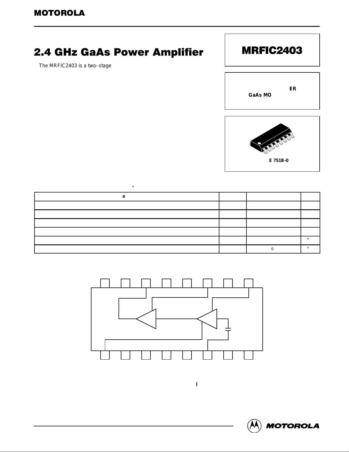
RF OUT
N/C GND GND GND V
16
15 14 13 12 11 10 9
V
D2
G2
DD
CONTRL
G2
A
stg
GND V
G1
_
C
_
C
REV 1
Motorola, Inc. 1995
1
V
DD
2 3 4 5 6 7 8
GND PCNTRL GND GND RF IN GND N/C
Pin Connections and Functional Block Diagram
MRFIC2403MOTOROLA RF DEVICE DATA
1
Page 2
RECOMMENDED OPERATING CONDITIONS
Parameter Symbol Value Unit
Supply Voltage V
Gate Bias Voltage, Input Stage V
Gate Bias Voltage, Output Stage V
Quiescent Drain Current, Stage One I
Quiescent Drain Current, Stage Two I
Operating Frequency Range f
DD
G1
G2
DQ1
DQ2
OP
4.75 to 5.25 Vdc
–1.0 Vdc
–2.0 Vdc
12 mA
10 mA
2200 to 2700 MHz
ELECTRICAL CHARACTERISTICS (V
5.0 Vdc)
Characteristic
Small Signal Gain (Pin = –6.0 dBm) – 23 – dB
Power Output (Pin = +4.0 dBm) 23 23.5 – dBm
Power Output, Saturation – 23.5 – dBm
Power Output, 1.0 dB Compression – 19 – dBm
2nd Harmonic Output – –20 – dBc
3rd Harmonic Output – –30 – dBc
Third Order Intermodulation Products (Pin = +4.0 dBm PEP) – –15 – dBc
Reverse Isolation – 32 – dB
Power Control Range, PCNTRL – 20 – dB
Reverse Isolation – 30 – dB
Supply Current – 95 140 mA
SLEEP Mode Supply Current (VG1 = VG2 = –3.0 Vdc, PCNTRL = 0 Vdc) – 150 –
V
G1
= 5.0 V d c , TA = 25_C, RF = 2.45 GHz @ +4.0 dBm, VG1 = –1.0 Vdc, VG2 = –2.0 Vdc, PCNTRL =
DD
Min Typ Max Unit
9
10
8
7
m
A
RF OUT
MRFIC2403
2
V
V
G2
DD2
C3
C6
C5
L1
C4
11
12
13
14
15
16
6
5
4
3
2
1
C2
C1
RF IN
PCNTRL
V
D1
Figure 1. Applications Circuit Configuration
C1, C2, C3 – 0.01 µF
C4 – 5.1 pF
C5 – 15 pF
C6 – 1.0 pF
L1 – 6.8 nH
Board Material – 30 MIL FR4
Connectors – SMA type
MOTOROLA RF DEVICE DATA
Page 3

(VDD = 5 V, I
T able 1. Class A Scattering Parameters
DQ1
= 24 mA, I
= 96 mA, TA = 25°C, 50 W System)
DQ2
f
(MHz) |S11| ∠ φ |S21| ∠ φ |S12| ∠ φ |S22| ∠ φ
2000 0.377 –157.00 27.625 57.40 0.004 –74.70 0.740 –102.10
2050 0.218 –171.70 28.938 36.80 0.006 –101.60 0.763 –115.30
2100 0.075 –178.80 29.088 17.20 0.007 –130.70 0.724 –126.80
2150 0.049 –96.10 27.904 –0.20 0.007 –163.20 0.663 –135.80
2200 0.104 –56.60 26.930 –14.90 0.008 –169.60 0.601 –141.80
2250 0.130 –60.60 24.246 –27.80 0.009 173.50 0.550 –146.30
2300 0.125 –65.40 24.286 –39.40 0.010 165.00 0.504 –149.10
2350 0.106 –67.60 22.287 –49.60 0.010 157.70 0.471 –151.60
2400 0.083 –56.10 21.867 –59.80 0.009 140.70 0.444 –153.80
2450 0.064 –27.00 21.837 –68.90 0.011 141.40 0.422 –155.90
2500 0.072 26.20 20.113 –78.00 0.012 139.80 0.401 –158.60
2550 0.110 44.60 19.828 –86.40 0.009 140.00 0.385 –161.20
2600 0.160 44.50 18.941 –94.30 0.007 124.50 0.364 –164.50
2650 0.194 40.60 18.001 –101.90 0.012 128.30 0.350 –167.70
2700 0.237 36.60 17.268 –109.20 0.011 102.30 0.335 –171.40
2750 0.269 31.30 16.379 –116.30 0.010 110.90 0.317 –174.50
2800 0.304 25.50 15.826 –123.40 0.009 105.80 0.311 –178.60
2850 0.325 19.80 15.125 –130.40 0.010 103.60 0.292 177.50
2900 0.345 14.50 14.611 –137.50 0.008 99.70 0.279 172.80
2950 0.356 9.40 14.048 –143.60 0.009 92.80 0.271 168.90
3000 0.370 2.40 13.663 –150.40 0.011 88.20 0.259 163.80
S
11
S
21
S
12
S
22
MRFIC2403MOTOROLA RF DEVICE DATA
3
Page 4

(VDD = 5 V, I
T able 2. Class B Scattering Parameters
DQ1
= 12 mA, I
= 10 mA, TA = 25°C, 50 W System)
DQ2
f
(MHz) |S11| ∠ φ |S21| ∠ φ |S12| ∠ φ |S22| ∠ φ
2000 0.634 –149.00 12.40 88.00 0.007 –59.00 0.893 –81.00
2050 0.554 –170.00 14.76 72.00 0.013 –81.00 0.966 –89.00
2100 0.456 163.00 17.00 53.00 0.015 –95.00 0.990 –100.00
2150 0.362 129.00 18.09 32.00 0.017 –1 17.00 0.955 –110.00
2200 0.310 91.00 18.81 12.00 0.020 –138.00 0.870 –119.00
2250 0.298 58.00 17.37 –5.00 0.021 –156.00 0.771 –125.00
2300 0.298 30.00 17.22 –21.00 0.021 –169.00 0.681 –128.00
2350 0.289 11.00 15.89 –34.00 0.020 179.00 0.612 –130.00
2400 0.275 0.00 14.74 –45.00 0.020 168.00 0.562 –130.00
2450 0.248 –8.00 15.35 –56.00 0.021 155.00 0.528 –131.00
2500 0.216 –10.00 13.62 –66.00 0.019 147.00 0.498 –131.00
2550 0.199 –8.00 13.46 –75.00 0.021 143.00 0.473 –132.00
2600 0.187 –2.00 12.95 –83.00 0.020 134.00 0.447 –132.00
2650 0.185 4.00 12.32 –91.00 0.020 129.00 0.426 –134.00
2700 0.202 10.00 11.78 –99.00 0.021 123.00 0.405 –135.00
2750 0.218 13.00 11.25 –107.00 0.021 115.00 0.384 –136.00
2800 0.244 14.00 10.83 –114.00 0.018 106.00 0.373 –137.00
2850 0.268 13.00 10.34 –121.00 0.019 98.00 0.353 –139.00
2900 0.285 10.00 10.05 –129.00 0.019 99.00 0.332 –140.00
2950 0.301 7.00 9.61 –135.00 0.018 102.00 0.316 –143.00
3000 0.317 3.00 9.46 –142.00 0.018 90.00 0.302 –145.00
S
11
S
21
S
12
S
22
MRFIC2403
4
MOTOROLA RF DEVICE DATA
Page 5

25
23
21
19
17
15
out
P , OUTPUT POWER (dBm)
13
11
–10
P
OUT
–6
PIN, INPUT POWER (dBm)
EFFICIENCY
f = 2.45 GHz
VDD = 5.0 Vdc
VG1 = –1.0 Vdc
VG2 = –2.0 Vdc
0
TYPICAL CHARACTERISTICS
70
60
50
40
30
20
10
0
6
26
25
24
23
22
21
20
out
P , OUTPUT POWER (dBm)
POWER ADDED EFFICIENCY (%)
19
18
2.1 2.3 2.5 2.7 2.9–8 –4 –2 2 4
TA = – 30°C
25°C
85°C
Pin = +4.0 dBm
VDD = 5.0 Vdc
VG1 = –1.0 Vdc
VG2 = –2.0 Vdc
3.02.82.22.0 2.62.4
f, FREQUENCY (GHz)
Figure 2. Output Power and Efficiency versus
Input Power
25
20
15
10
5
, OUTPUT POWER (dBm)
out
P
0
–5
1
PCNTRL, (VOLTS)
Figure 4. Output Power versus PCNTRL Voltage
DESIGN AND APPLICATIONS INFORMATION
The MRFIC2403 is a two–stage power amplifier designed
using Motorola’s MAFET planar, refractory gate MESFET IC
process. The RF MESFETs are power, depletion mode
devices and, therefore, require negative bias on the MESFET
gates. For class B operation, –1.0 Vdc is applied to VG1 and
–2.0 Vdc is applied to VG2. Class A biasing will yield slightly
higher gain and 1.0 dB compression point and can be accomplished by adjusting the bias on VG1 for I
VG2 for I
= 96 mA. Where negative voltages are not
DQ2
= 24 mA and
DQ1
already available, Motorola’s MC33128 Power Management
IC can produce –2.5 Vdc from a single positive supply .
The device is capable of better than +23 dBm saturated
output power in the 2.4 to 2.5 GHz ISM band with the output
matching circuit shown in Figure 1. The device can be
operated at other frequencies in the 2.0 GHz to 3.0 GHz
range with this circuit but performance can be improved
with tuning for the specific frequency of use. Input matching is provided on chip. This circuit provides the best gain,
saturated output power and efficiency tradeoff. Saturated
operation has the advantage of best efficiency with less
variation in performance over frequency and temperature.
Operation in saturation is acceptable for constant envelope modulation schemes such as 2 and 4 level FM as spe cified for frequency hopping (FHSS) radios in the proposed
IEEE 802.11 PHY layer specification. For direct sequence
Figure 3. Output Power versus Frequency
f = 2.45 GHz
Pin = +4.0 dBm
VDD = 5.0 Vdc
VG1 = –1.0 Vdc
VG2 = –2.0 Vdc
3
4
520
(DSSS) IEEE 802.11 operation, where differential binary
phase shift keying (DBPSK) and differential quadrature
phase shift keying (DQPSK) are specified, the amplifier will
have to be “backed off” from saturation by 5.0 dB or more to
avoid spectral regrowth. Care must be taken in the layout of
the circuit and controlled impedance lines must be used at
the RF pins. Capacitive bypassing as shown in the Applications Circuit must be implemented as close to the chip as
possible to avoid amplifier instability. Additionally, the supply
voltage should be supported by sufficient “stiffening” capacitance, typically electrolytic or tantalum bypass capacitors, to
eliminate noise from digital circuits.
Output power control is accomplished by varying the voltage on the PCNTRL pin. 0 Vdc gives minimum output and
reduces the current drawn by the amplifier to the quiescent
value. The amplifier can be put into “sleep” mode by
decreasing the voltage on the gate bias pins to –3.0 Vdc and
the current drain is reduced to a few hundred microamps.
EVALUATION BOARDS
Evaluation boards are available for RF Monolithic Integrated Circuits by adding a “TF” suffix to the device type.
For a complete list of currently available boards and ones
in development for newly introduced poduct, please contact your local Motorola Distributor or Sales Office.
MRFIC2403MOTOROLA RF DEVICE DATA
5
Page 6

P ACKAGE DIMENSIONS
–T–
–A–
16 9
–B–
18
8 PLP
0.25 (0.010) B
G
K
C
SEATING
PLANE
D
16 PL
0.25 (0.010) A
M
S
B
T
M
S
CASE 751B–05
ISSUE J
NOTES:
1. DIMENSIONING AND TOLERANCING PER ANSI
Y14.5M, 1982.
2. CONTROLLING DIMENSION: MILLIMETER.
3. DIMENSIONS A AND B DO NOT INCLUDE
MOLD PROTRUSION.
4. MAXIMUM MOLD PROTRUSION 0.15 (0.006)
PER SIDE.
M
S
R
X 45
_
F
J
5. DIMENSION D DOES NOT INCLUDE DAMBAR
PROTRUSION. ALLOWABLE DAMBAR
PROTRUSION SHALL BE 0.127 (0.005) TOTAL
IN EXCESS OF THE D DIMENSION AT
MAXIMUM MATERIAL CONDITION.
DIM MIN MAX MIN MAX
A 9.80 10.00 0.386 0.393
B 3.80 4.00 0.150 0.157
C 1.35 1.75 0.054 0.068
D 0.35 0.49 0.014 0.019
F 0.40 1.25 0.016 0.049
G 1.27 BSC 0.050 BSC
J 0.19 0.25 0.008 0.009
K 0.10 0.25 0.004 0.009
M 0 7 0 7
____
P 5.80 6.20 0.229 0.244
R 0.25 0.50 0.010 0.019
INCHESMILLIMETERS
Motorola reserves the right to make changes without further notice to any products herein. Motorola makes no warranty, representation or guarantee regarding
the suitability of its products for any particular purpose, nor does Motorola assume any liability arising out of the application or use of any product or circuit,
and specifically disclaims any and all liability, including without limitation consequential or incidental damages. “T ypical” parameters can and do vary in different
applications. All operating parameters, including “T ypicals” must be validated for each customer application by customer’s technical experts. Motorola does
not convey any license under its patent rights nor the rights of others. Motorola products are not designed, intended, or authorized for use as components in
systems intended for surgical implant into the body, or other applications intended to support or sustain life, or for any other application in which the failure of
the Motorola product could create a situation where personal injury or death may occur. Should Buyer purchase or use Motorola products for any such
unintended or unauthorized application, Buyer shall indemnify and hold Motorola and its officers, employees, subsidiaries, affiliates, and distributors harmless
against all claims, costs, damages, and expenses, and reasonable attorney fees arising out of, directly or indirectly, any claim of personal injury or death
associated with such unintended or unauthorized use, even if such claim alleges that Motorola was negligent regarding the design or manufacture of the part.
Motorola and are registered trademarks of Motorola, Inc. Motorola, Inc. is an Equal Opportunity/Af firmative Action Employer.
How to reach us:
USA/ EUROPE: Motorola Literature Distribution; JAPAN: Nippon Motorola Ltd.; Tatsumi–SPD–JLDC, Toshikatsu Otsuki,
P.O. Box 20912; Phoenix, Arizona 85036. 1–800–441–2447 6F Seibu–Butsuryu–Center, 3–14–2 Tatsumi Koto–Ku, Tokyo 135, Japan. 03–3521–8315
MFAX: RMF AX0@email.sps.mot.com – T OUCHTONE (602) 244–6609 HONG KONG: Motorola Semiconductors H.K. Ltd.; 8B Tai Ping Industrial Park,
INTERNET: http://Design–NET.com 51 Ting K ok Road, T ai Po, N.T., Hong Kong. 852–26629298
MRFIC2403
6
◊
MOTOROLA RF DEVICE DATA
*MRFIC2403/D*
MRFIC2403/D
 Loading...