

Page 1
SEMICONDUCTOR TECHNICAL DATA
The MRFIC Line
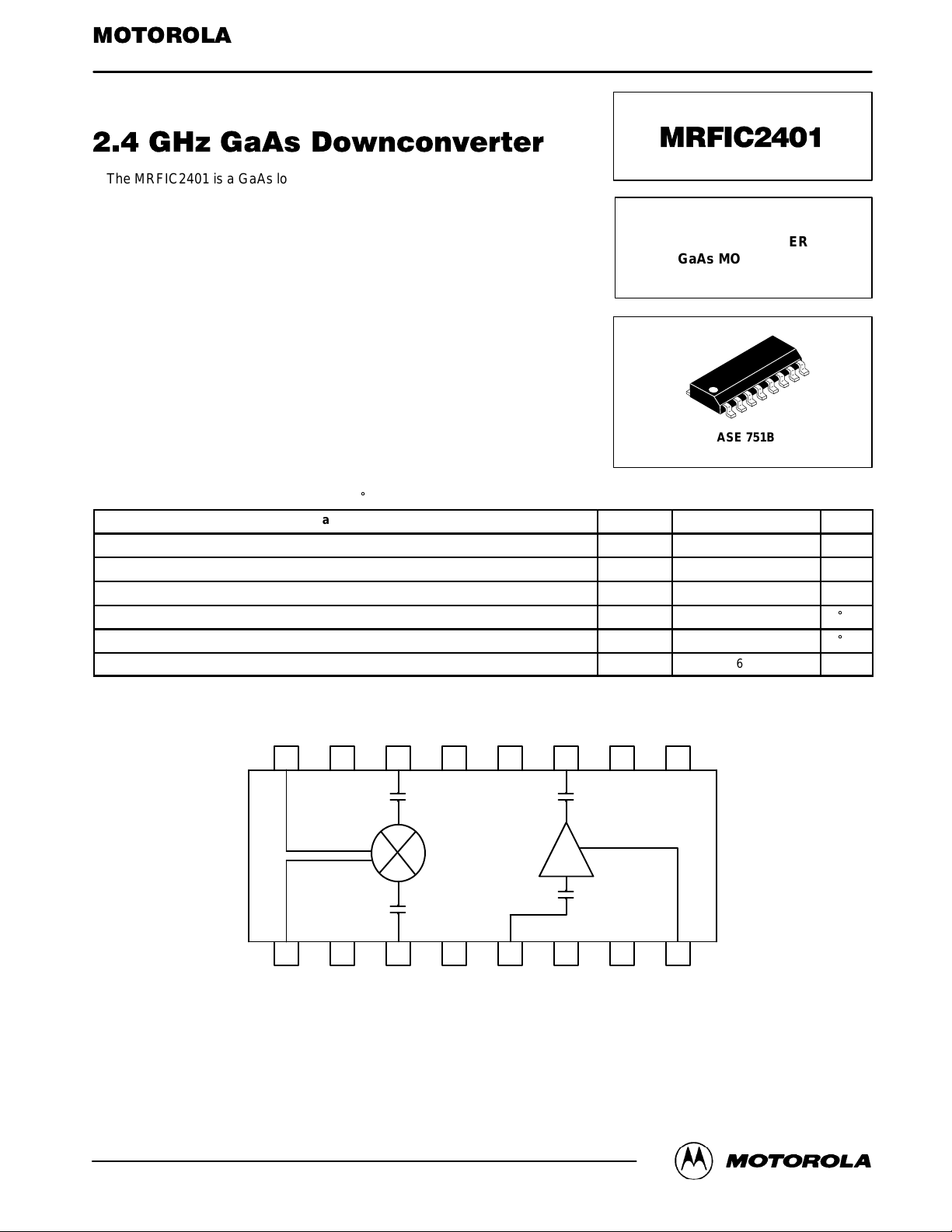
The MRFIC2401 is a GaAs low–noise amplifier and downmixer in a low–cost
16 lead plastic package designed for use in the 2.4 to 2.5 GHz Industrial–
Scientific–Medical (ISM) band. The design is optimized for efficiency at 5.0 V olt
operation at 2.45 GHz but is usable from 2.0 to 3.0 GHz in applications such as
telemetry and Multichannel Multipoint Distribution System (MMDS) wireless
cable TV systems. Performance is suitable for frequency hopping or direct
sequence spread spectrum as well as single–frequency applications. LNA
output and mixer input are available to allow image filtering.
• Single Supply Voltage = 5.0 Volts
• High Conversion Gain = 21 dB Typical Less Image Filter
• Low Supply Current = 9.5 mA Typical
• Low–Cost, Low Profile Plastic SOIC Package
• Available in Tape and Reel by Adding R2 Suffix to Part Number.
R2 Suffix = 2,500 Units per 16 mm, 13 inch Reel.
• Device Marking = M2401
Order this document
by MRFIC2401/D
2.4 GHz
DOWNCONVERTER
GaAs MONOLITHIC
INTEGRATED CIRCUIT
CASE 751B-05
(SO-16)
ABSOLUTE MAXIMUM RATINGS
Supply Voltage V
Input Power, RF IN Ports P
Input Power, LO IN Port P
Ambient Operating Temperature T
Storage Temperature T
Bias Control Voltage STANDBY 6.0 Vdc
(TA = 25_C unless otherwise noted)
Parameter Symbol Value Unit
6.0 Vdc
+5.0 dBm
+5.0 dBm
–30 to +85
–65 to +125
IF
OUT
16
DD
RF
LO
A
stg
RF IN
GND
MIXER
15 14 13 12 11 10 9
GND
MIXER
V
DD
RF OUT
LNA
GND STANDBY
_
C
_
C
REV 3
Motorola, Inc. 1995
1
MIXER
V
DD
2 3 4 5 6 7 8
GND LO IN GND GNDRF IN
LNA
GND LNA
Pin Connections and Functional Block Diagram
V
DD
SLEEP
MRFIC2401MOTOROLA RF DEVICE DATA
1
Page 2
RECOMMENDED OPERATING CONDITIONS
Parameter Symbol Value Unit
Supply Voltage V
IF Frequency Range f
LO Drive Power Level P
LO Frequency Range f
RF Frequency Range f
STANDBY Mode ON STANDBY V
STANDBY Mode OFF STANDBY 0 Vdc
SLEEP Mode OFF SLEEP V
SLEEP Mode ON SLEEP 0 Vdc
DD
IF
LO
LO
RF
4.75 to 5.25 Vdc
100 to 350 MHz
–10 to 0 dBm
2050 to 2400 MHz
2400 to 2500 MHz
DD
DD
Vdc
Vdc
ELECTRICAL CHARACTERISTICS (V
Characteristic Min Typ Max Unit
Conversion Gain – Downconverter (Less Image Filter Loss) 19 21 – dB
Gain – LNA – 17 – dB
Conversion Gain – Mixer – 4.0 – dB
Noise Figure – LNA – 1.9 – dB
Noise Figure – Mixer – 11 – dB
Return Loss – Mixer Input, LO Input, LNA Output – 10 – dB
Input Third Order Intercept – Downconverter (Less Image Filter Loss) – –18 – dBm
Input Third Order Intercept – LNA – –13 – dBm
Input Third Order Intercept – Mixer – 0 – dBm
Reverse Isolation – Downconverter (Less Image Filter Loss) – 30 – dB
Isolation – LO to RF, LO to IF – 20 – dB
Supply Current – Downconverter – 9.5 11 mA
SLEEP Mode Supply Current – Downconverter
(No LO, STANDBY= 5 Vdc, VDD/SLEEP = 5 Vdc)
Turn On, Turn Off Time – LNA – 1.0 –
= 5.0 Vdc, TA = 25_C, RF = 2.45 GHz, LO = 2.125 GHz @ –5.0 dBm, STANDBY = 0 Vdc)
DD
– 600 –
m
A
m
s
MRFIC2401
2
MOTOROLA RF DEVICE DATA
Page 3
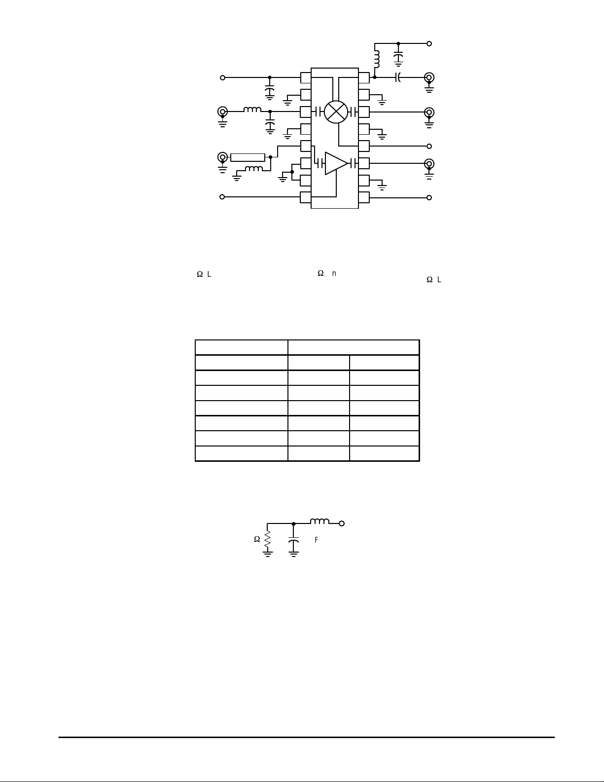
L2
C2
V
DD
MIXER V
DD
LO IN
LNA IN
LNA VDD/
SLEEP
325 MHz IF:
C1, C2 – 100 pF
C3 – 5.6 pF
C4 – 0.5 pF
L1 – 4.7 nH
L2 – 8.2nH
L3 – 6.8 nH
T1 – 100 Line, 92 MILS
T1
Figure 1. Applications Circuit Configuration
f LO Z
Frequency (GHz) R jX
2.0 39.7 23.9
2.1 35.7 22.1
2.2 32.1 19.8
2.3 29.1 17.1
2.4 26.5 14.0
2.5 24.4 10.7
T able 1. Selected Port Impedances
1
C1
L1
C4
L3
2
3
4
5
6
7
8
240 MHz IF:
C1, C2 – 100 pF
C3 – 5.6 pF
C4 – 0.5 pF
L1 – 8.2 nH
L2 – 18 nH
L3 – 6.8 nH
T1 – 100 Line, 92mils
Board Material – FR4
(from Conjugate Match)
16
15
14
13
12
11
10
9
in
C3
110 MHz IF:
C1 – 100 pF
C2 – 1000 pF
C3 – 8.2 pF
C4 – 0.3 pF
L1 – 8.2 nH
L2 – 82 nH
L3 – 6.8 nH
T1 – 100 Line, 92 mils
IF OUT
RF IN
MIXER V
DD
LNA OUT
STANDBY
1.0 nH
IF OUT
500
15 pF
Figure 2. Equivalent IF Output Circuit
MRFIC2401MOTOROLA RF DEVICE DATA
3
Page 4

T able 2. LNA Scattering Parameters
(VDD = 5 V, TA = 25°C, 50 W System)
f
(MHz) |S11| ∠ φ |S21| ∠ φ |S12| ∠ φ |S22| ∠ φ
2000 0.823 –50.8 5.35 14.3 0.0373 164.2 0.609 –64.1
2050 0.783 –62.9 6.13 –0.3 0.0425 154.3 0.558 –78.7
2100 0.752 –76.8 6.56 –18.3 0.0477 138 0.497 –94.3
2150 0.713 –89.8 6.8 –34 0.05 121 0.425 –110.7
2200 0.656 –104.2 7.14 –50.2 0.0511 106.4 0.343 –129.6
2250 0.583 –119 7.44 –66.4 0.0527 91.8 0.25 –152.3
2300 0.509 –134.1 7.8 –84.2 0.0554 78.1 0.155 176.2
2350 0.425 –148.2 7.86 –102.6 0.0579 59.89 0.088 120.7
2400 0.34 –163.6 7.84 –119.4 0.0552 42.31 0.111 43.8
2450 0.261 –177.8 7.78 –138.1 0.0528 28.27 0.191 2.2
2500 0.175 173.4 7.43 –154.6 0.0514 13.37 0.269 –21.9
2550 0.103 170.4 7.15 –170.6 0.0484 –0.842 0.338 –41.8
2600 0.056 –160.5 6.72 173 0.0455 –15.4 0.393 –59.4
2650 0.067 –130.7 6.47 159.1 0.0422 –28.1 1 0.436 –76.2
2700 0.102 –117.8 6.25 142.3 0.039 –41.5 0.472 –92.2
2750 0.132 –119.5 5.53 127.1 0.0353 –53.47 0.496 –107.5
2800 0.166 –125.2 5.26 117.5 0.0329 –63.28 0.513 –121.3
2850 0.19 –134.8 5.15 102.4 0.0309 –75.04 0.533 –135
2900 0.219 –144.8 4.71 87.6 0.0283 –87.86 0.547 –148.8
2950 0.235 –155.9 4.43 76.1 0.025 –95.83 0.559 –162.4
3000 0.262 –165.9 4.08 62.3 0.0235 –108.4 0.57 –175.7
S
11
S
21
S
12
S
22
MRFIC2401
4
MOTOROLA RF DEVICE DATA
Page 5

30
25
20
15
SSB GAIN (dB)
IF = 325 MHz
Pin = – 40 dBm
VDD = 5.0 Vdc
10
5
25°C
+85°C
2.7
f, FREQUENCY (GHz)
TYPICAL CHARACTERISTICS
0
–2
TA = – 30°C
3.02.42.0
–4
–6
–8
–10
IF = 325 MHz
–12
0 dB FILTER LOSS
1.0 dB COMPRESSION (dB)
VDD = 5.0 Vdc
–14
–16
–18
2.1 2.3 2.5 2.7 2.92.1 2.2 2.3 2.5 2.6 2.8 2.9
25°C
+85°C
f, FREQUENCY (GHz)
TA = – 30°C
3.02.82.22.0 2.62.4
Figure 3. Downconverter Gain versus Frequency
20
19
18
17
16
15
14
G, GAIN (dB)
13
Pin = – 25 dBm
12
VDD = 5.0 Vdc
11
10
NF
f, FREQUENCY (GHz)
GAIN
2.6
Figure 5. LNA Gain and Noise Figure
versus Frequency
10
2.8
Figure 4. Downconverter 1.0 dB Compression
versus Frequency
2.4
2.2
2.0
1.8
1.6
1.4
2.92.2 2.5 2.72.1 2.4
3.02.32.0
0
–5
–10
–15
, OUTPUT POWER (dBm)
out
p
SSB NOISE FIGURE (dB)
–20
–25
–35 –25
f = 2.45 GHz
VDD = 5.0 Vdc
–10–15–30–40 –20
Pin, INPUT POWER (dBm)
Figure 6. LNA Output Power versus Input Power
–1
8
6
4
2
SSB GAIN (dB)
0
IF = 325 MHz
Pin = 20 dBm
–2
VDD = 5.0 Vdc
–4
Plo = – 5.0 dBm
–6
25°C
TA = – 30°C
+85°C
2.72.1 2.52.3
f, FREQUENCY (GHz)
Figure 7. Mixer Conversion Gain
versus Frequency
2.9
–3
–5
–7
–9
IF = 325 MHz
Pin = – 20 dBm
–11
VDD = – 5.0 Vdc
1.0 dB COMPRESSION (dBm)
Plo = – 5.0 dBm
–13
3.02.82.22.0 2.62.4
–15
25°C
+85°C
f, FREQUENCY (GHz)
TA = – 30°C
2.92.72.32.1 2.5
3.02.82.42.22.0 2.6
Figure 8. Mixer 1.0 dB Compression
versus Frequency
MRFIC2401MOTOROLA RF DEVICE DATA
5
Page 6

11
10
9
8
7
6
SSB GAIN (dB)
5
4
3
2
–10
TYPICAL CHARACTERISTICS
–1
–2
0–6
–3
–4
–5
–6
–7
–8
–9
–10
1.0 dB COMP f = 325 MHz
GAIN
IF = 325 MHz
RF = 2.45 GHz
VDD = 5.0 Vdc
–3
LO INPUT POWER (dBm)
8
6
4
2
0
–2
G, GAIN (dB)
–4
1.0 dB COMPRESSION (dB)
–6
–8
–10
240 MHz
RF = 2.45 GHz
Pin = – 20 dBm
VDD = 5.0 Vdc
2.1 2.3 2.5 2.7 2.9–9 –8 –7 –5 –4 –2 –1
110 MHz
f, FREQUENCY (GHz)
3.02.82.22.0 2.62.4
Figure 9. Mixer 1.0 dB Compression and Gain
Figure 10. Mixer Gain versus Frequency
versus LO Power
16
15
14
13
12
SSB NF (dB)
11
10
9
2.6
f, FREQUENCY (dB)
IF = 325 MHz
VDD = 5.0 Vdc
2.9
2.82.2 2.5 2.72.1 2.4
3.02.32.0
–22
–24
–26
–28
–30
–32
LO FEEDTHROUGH (dBm)
IF = 325 MHz
VDD = 5.0 Vdc
–34
Plo = – 5.0 dBm
–36
+85°C
RF FREQUENCY (GHz)
TA = – 30°C
2.72.1 2.52.3
Figure 11. Mixer Noise Figure versus Frequency Figure 12. Mixer LO Feedthrough versus
RF Frequency
25°C
2.9
3.02.82.22.0 2.62.4
MRFIC2401
6
MOTOROLA RF DEVICE DATA
Page 7

DESIGN AND APPLICATIONS INFORMATION
The MRFIC2401 consists of a two–stage GaAs MESFET
low noise amplifier and a single ended MESFET mixer. The
LNA design conserves bias current through stacking of the
two FETs, thus reusing the current. The mixer consists of a
common gate stage driving a common source stage with the
IF output being the drain of the common source stage
shunted with 15 pF. The LNA output and mixer input have
been separated to allow the addition of an external image filter. Such a filter, usually ceramic, is useful in improving the
mixer noise figure and third order intercept performance. It
also provides LO rejection to reduce the amount of LO power
which may leak to the antenna. Alternatively, image trapping
can be implemented at the LNA input or output with discrete
or distributed components.
The design has been optimized for best performance from
2.4 to 2.5 GHz, but the device is usable with reduced performance from 2.0 to 3.0 GHz as shown in the performance
curves. These curves were generated using the circuit
shown in Figure 1 and performance above 2.5 GHz can be
enhanced by rematching the LO input port. Matching circuit
details are shown for IFs of 110 MHz, 240 MHz, and
325 MHz matched to 50 W and LO frequencies consistent
with an RF frequency of 2.45 GHz. Customized IF matching
can be accomplished by using the Equivalent IF Output circuit model shown in Figure 2. The best gain/noise figure
tradeoff match is shown in the LNA input impedance column
of Table 1. The LO input impedance is shown in the same
table. These numbers are derived from conjugate match
measurements of the applications circuit. The LNA output
and mixer input are matched to 50 W.
As with all RF circuitry, layout is important. Controlled
impedance lines should be used at all RF ports. RF bypassing of power supply connections as close to the part as possible, while not always shown in the applications circuit, are
recommended. Additional power supply “stiffening” and digital transient bypassing should be accomplished with electrolytic or tantalum capacitors.
The device can be placed in a reduced current “standby”
mode by applying 5.0 Vdc to the STANDBY pin and removing the LO drive. Further current reduction “sleep” mode, is
enabled by applying 0 Vdc to VDD/SLEEP. This sleep mode
can also be used to disable the LNA under high signal level
conditions and give higher input intercept point if VDD is still
applied to the mixer.
EVALUATION BOARDS
Evaluation boards are available for RF Monolithic Integrated Circuits by adding a “TF” suffix to the device type.
For a complete list of currently available boards and ones
in development for newly introduced poduct, please contact your local Motorola Distributor or Sales Office.
MRFIC2401MOTOROLA RF DEVICE DATA
7
Page 8

P ACKAGE DIMENSIONS
–T–
–A–
16 9
–B–
18
8 PLP
0.25 (0.010) B
G
K
C
SEATING
PLANE
D
16 PL
0.25 (0.010) A
M
S
B
T
M
S
CASE 751B–05
M
R
X 45
ISSUE J
NOTES:
1. DIMENSIONING AND TOLERANCING PER ANSI
Y14.5M, 1982.
2. CONTROLLING DIMENSION: MILLIMETER.
3. DIMENSIONS A AND B DO NOT INCLUDE
MOLD PROTRUSION.
4. MAXIMUM MOLD PROTRUSION 0.15 (0.006)
PER SIDE.
S
_
F
J
5. DIMENSION D DOES NOT INCLUDE DAMBAR
PROTRUSION. ALLOWABLE DAMBAR
PROTRUSION SHALL BE 0.127 (0.005) TOTAL
IN EXCESS OF THE D DIMENSION AT
MAXIMUM MATERIAL CONDITION.
DIM MIN MAX MIN MAX
A 9.80 10.00 0.386 0.393
B 3.80 4.00 0.150 0.157
C 1.35 1.75 0.054 0.068
D 0.35 0.49 0.014 0.019
F 0.40 1.25 0.016 0.049
G 1.27 BSC 0.050 BSC
J 0.19 0.25 0.008 0.009
K 0.10 0.25 0.004 0.009
M 0 7 0 7
____
P 5.80 6.20 0.229 0.244
R 0.25 0.50 0.010 0.019
INCHESMILLIMETERS
Motorola reserves the right to make changes without further notice to any products herein. Motorola makes no warranty, representation or guarantee regarding
the suitability of its products for any particular purpose, nor does Motorola assume any liability arising out of the application or use of any product or circuit,
and specifically disclaims any and all liability, including without limitation consequential or incidental damages. “T ypical” parameters can and do vary in different
applications. All operating parameters, including “T ypicals” must be validated for each customer application by customer’s technical experts. Motorola does
not convey any license under its patent rights nor the rights of others. Motorola products are not designed, intended, or authorized for use as components in
systems intended for surgical implant into the body, or other applications intended to support or sustain life, or for any other application in which the failure of
the Motorola product could create a situation where personal injury or death may occur. Should Buyer purchase or use Motorola products for any such
unintended or unauthorized application, Buyer shall indemnify and hold Motorola and its officers, employees, subsidiaries, affiliates, and distributors harmless
against all claims, costs, damages, and expenses, and reasonable attorney fees arising out of, directly or indirectly, any claim of personal injury or death
associated with such unintended or unauthorized use, even if such claim alleges that Motorola was negligent regarding the design or manufacture of the part.
Motorola and are registered trademarks of Motorola, Inc. Motorola, Inc. is an Equal Opportunity/Af firmative Action Employer.
How to reach us:
USA/ EUROPE: Motorola Literature Distribution; JAPAN: Nippon Motorola Ltd.; Tatsumi–SPD–JLDC, Toshikatsu Otsuki,
P.O. Box 20912; Phoenix, Arizona 85036. 1–800–441–2447 6F Seibu–Butsuryu–Center, 3–14–2 Tatsumi Koto–Ku, Tokyo 135, Japan. 03–3521–8315
MFAX: RMF AX0@email.sps.mot.com – T OUCHTONE (602) 244–6609 HONG KONG: Motorola Semiconductors H.K. Ltd.; 8B Tai Ping Industrial Park,
INTERNET: http://Design–NET.com 51 Ting K ok Road, T ai Po, N.T., Hong Kong. 852–26629298
MRFIC2401
8
◊
MOTOROLA RF DEVICE DATA
*MRFIC2401/D*
MRFIC2401/D
 Loading...