

Page 1
SEMICONDUCTOR TECHNICAL DATA
The MRFIC Line
The MRFIC2006 is an Integrated P A designed for linear operation in the 800
MHz to 1.0 GHz frequency range. The design utilizes Motorola’s advanced
MOSAIC 3 silicon bipolar RF process to yield superior performance in a cost
effective monolithic device. Applications for the MRFIC2006 include CT-1 and
CT-2 cordless telephones, remote controls, video and audio short range links,
low cost cellular radios, and ISM band transmitters.
• 50 Ω Input and Output Impedance
• Typical Gain = 23 dB @ 900 MHz
• Bias Current Externally Adjustable
• Bias Pin can be used to Ramp or Disable
• Class A or AB Linear Operation
• Unconditionally Stable
• SO-8 Leaded Plastic Package
• Order MRFIC2006R2 for Tape and Reel.
R2 Suffix = 2,500 Units per 12 mm, 13 inch Reel.
• Device Marking = M2006
Order this document
by MRFIC2006/D
900 MHz 2 STAGE PA
SILICON MONOLITHIC
INTEGRATED CIRCUIT
CASE 751-05
(SO-8)
ABSOLUTE MAXIMUM RATINGS
Supply Voltages V
Bias Voltage V
Total Supply Current I
RF Output Power (V
RF Output Power (4.0 V < V
RF Input Power P
Operating Ambient Temperature T
Storage and Junction Temperature T
Thermal Resistance, Junction to Case R
< 4.0 V) P
CC2
CC2
(TA = 25°C, Zo = 50 Ω unless otherwise noted)
Rating Symbol Value Unit
≤ 5.0 V) P
GND
4
GND
3
GND
2
, V
CC1
bias
, I
CC1
out
out
in
A
stg
θJC
RF OUT
1
CC2
CC2
(V
CC2
5.0 Vdc
6.0 Vdc
100 mA
+21 dBm
53 – 8 V
CC2
+10 dBm
– 35 to + 85 °C
– 65 to +150 °C
63 °C/W
)
dBm
REV 2
Motorola, Inc. 1997
V
8
bias
5
RF IN
6
GND
V
7
CC1
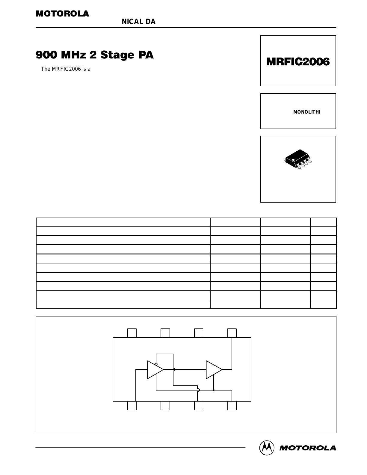
Pin Connections and Functional Block Diagram
MRFIC2006MOTOROLA RF DEVICE DATA
1
Page 2
RECOMMENDED OPERATING RANGES
Parameter Symbol Value Unit
Supply Voltage Ranges V
Bias Voltage Range V
RF Frequency Range f 500 to 1000 MHz
ELECTRICAL CHARACTERISTICS (V
Characteristics (1)
Supply Current — Total — 46 55 mA
I
CC1
I
CC2
I Bias — 3.0 — mA
Small Signal Gain 19 23 26 dB
Input Return Loss, RF IN Port — 15 — dB
Output Return Loss, RF OUT Port — 15 — dB
Reverse Isolation — 35 — dB
Output Power at 1.0 dB Gain Compression +12 +15.5 — dBm
3rd Order Intercept Point (Out) — +25 — dBm
5th Order Intercept Point (Out) — +21 — dBm
NOTE:
1. All electrical characteristics measured in test circuit schematic shown in Figure 1 below.
CC1
, V
CC2
, V
= 3.0 V, TA = 25°C, f = 900 MHz, Zo = 50 Ω unless otherwise noted)
bias
, V
CC1
CC2
bias
Min Typ Max Unit
— 14 — mA
— 29 — mA
1.8 to 4.0 Vdc
0 to 5.0 Vdc
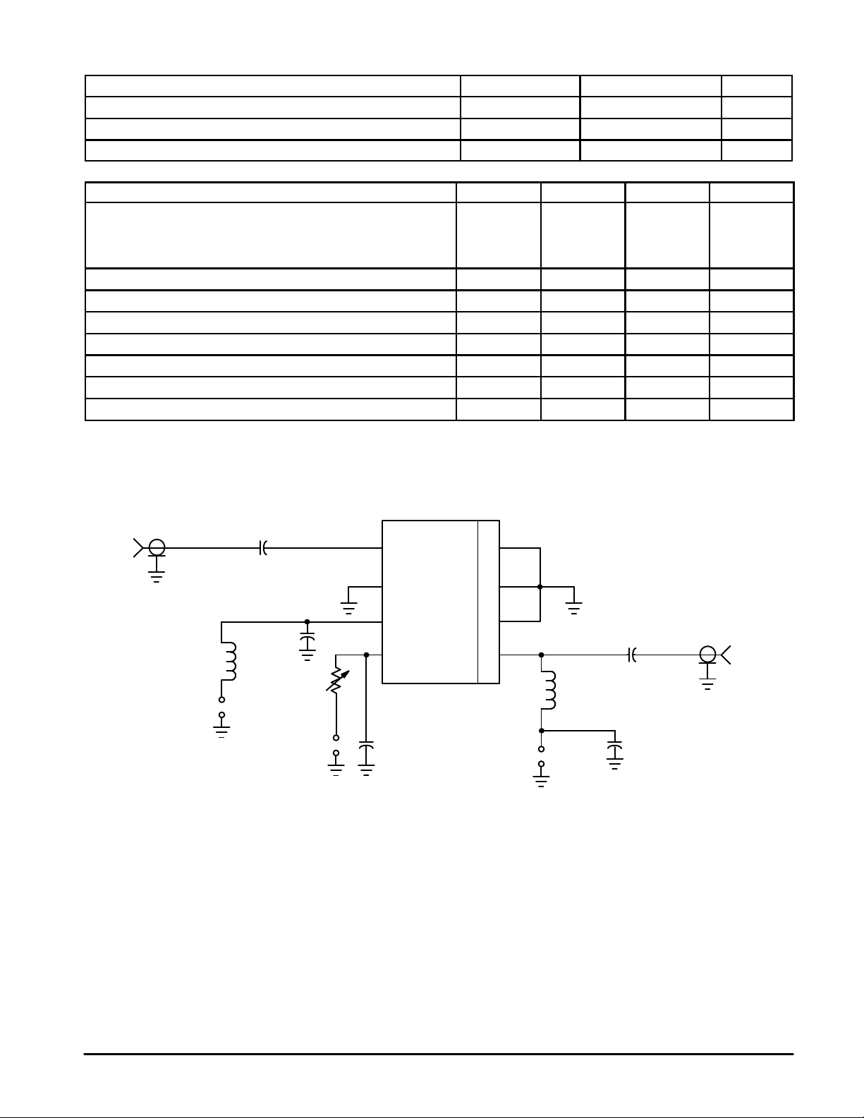
RF IN
50
Ω
C1
C3
L1
R1
+
V
CC1
–
+
V
bias
–
C1, C2 — 100 pF Chip Capacitor
C3, C5 — 1.0 nF Chip Capacitor
C4 — 10 nF Chip Capacitor
L1 — 150 nH Chip Inductor
L2 — 10 nH Chip Inductor
Figure 1. T ypical Biasing Configuration
C4
5
6
DUT
7
8
4
3
2
C2
1
L2
+
V
CC2
–
R1 — Resistor Optional
RF Connectors — SMA Type
Board Material — Epoxy/Glass εr = 4.5,
Dielectric Thickness = 0.014″ (0.36 mm)
C5
RF OUT
50
Ω
MRFIC2006
2
MOTOROLA RF DEVICE DATA
Page 3

T able 1. Scattering Parameters for 900 MHz Two–Stage PA
(V
, V
, V
CC1
CC2
= 3 V, I = 49 mA, TA = 25°C, 50 W System)
BIAS
f
(MHz) |S11| ∠ φ |S21| ∠φ |S12| ∠φ |S22| ∠ φ
50 0.739 –16.67 3.785 51.56 0.003 –163.12 0.461 –89.23
100 0.702 –24.53 5.772 46.52 0.001 15.96 0.354 –117.30
150 0.671 –33.09 7.901 40.16 0.001 84.34 0.263 –144.77
200 0.649 –41.55 10.065 32.12 0.001 –165.89 0.208 –167.08
250 0.630 –49.79 12.287 23.06 0.002 –159.68 0.169 170.65
300 0.610 –58.60 14.576 12.25 0.002 171.75 0.136 145.40
350 0.592 –67.09 16.834 1.32 0.003 –160.23 0.113 113.52
400 0.567 –75.32 19.009 –10.72 0.005 –167.93 0.105 73.18
450 0.537 –83.69 20.901 –23.88 0.005 167.71 0.122 33.86
500 0.495 –91.79 22.237 –37.89 0.007 159.88 0.157 2.30
525 0.470 –95.35 22.626 –45.02 0.007 168.37 0.178 –10.93
550 0.448 –98.65 22.821 –52.22 0.010 162.65 0.196 –22.73
575 0.421 –101.69 22.834 –59.20 0.009 159.52 0.216 –32.62
600 0.397 –104.40 22.647 –66.13 0.010 155.15 0.233 –42.62
625 0.371 –106.50 22.299 –73.01 0.011 151.24 0.246 –50.98
650 0.349 –108.28 21.813 –79.43 0.011 148.14 0.258 –59.21
675 0.329 –109.85 21.204 –85.70 0.012 145.35 0.269 –66.61
700 0.310 –111.02 20.538 –91.62 0.012 140.66 0.273 –73.29
725 0.293 –111.65 19.824 –97.20 0.014 136.88 0.280 –79.97
750 0.278 –112.24 19.094 –102.54 0.014 136.98 0.281 –85.86
775 0.265 –112.60 18.334 –107.76 0.014 134.67 0.285 –91.50
800 0.252 –112.81 17.594 –112.54 0.016 133.71 0.284 –96.72
825 0.242 –113.50 16.880 –117.13 0.015 129.16 0.282 –102.24
850 0.233 –114.93 16.127 –122.44 0.017 131.80 0.281 –107.68
875 0.224 –115.32 15.438 –126.92 0.017 126.66 0.279 –112.88
900 0.216 –116.04 14.796 –130.89 0.017 127.06 0.275 –117.56
925 0.210 –116.66 14.165 –134.57 0.018 121.77 0.273 –120.85
950 0.203 –117.91 13.555 –138.19 0.019 122.40 0.269 –125.53
975 0.195 –118.87 13.009 –141.73 0.019 120.80 0.265 –129.73
1000 0.191 –120.47 12.515 –145.08 0.019 122.53 0.265 –132.68
1025 0.186 –122.39 12.004 –148.23 0.020 119.56 0.259 –137.22
1050 0.179 –124.03 11.517 –151.36 0.022 115.24 0.254 –140.85
1075 0.175 –126.22 11.063 –154.40 0.022 117.88 0.251 –144.69
1100 0.168 –128.77 10.634 –157.40 0.024 112.04 0.248 –148.25
1125 0.163 –131.41 10.228 –160.15 0.023 112.42 0.246 –151.75
1150 0.161 –133.93 9.841 –163.04 0.023 115.77 0.245 –155.28
1175 0.155 –136.68 9.479 –165.88 0.025 110.34 0.241 –158.69
1200 0.152 –140.85 9.125 –168.50 0.025 109.94 0.241 –161.95
S
11
S
21
S
12
S
22
MRFIC2006MOTOROLA RF DEVICE DATA
3
Page 4

TYPICAL CHARACTERISTICS
28
26
24
G, GAIN (dB)
22
20
20
15
10
out
5
P , OUTPUT POWER (dBm)
V
, V
CC1
CC2
TA = –35°C
25°C
f, FREQUENCY (MHz)
+85°C
Figure 2. Gain versus Frequency
TA = –35°C
85°C
f = 900 MHz
V
, V
CC1
25°C
CC2
, V
, V
bias
bias
= 3 V
= 3 V
1000900800700600500
28
26
24
22
G, GAIN (dB)
20
18
25
20
15
10
out
P , OUTPUT POWER (dBm)
5
V
, V
CC1
3 V
3 V
2 V
f, FREQUENCY (MHz)
CC2
Figure 3. Gain versus Frequency
V
, V
, V
CC1
CC2
bias
= 4 V
3 V
2 V
f = 900 MHz
TA = 25
TA = 25°C
, V
bias
°
= 4 V
1000900800700600500
C
0
–20
–15 –10 –5 0 5
Pin, INPUT POWER (dBm)
Figure 4. Output Power versus Input Power
0
–5
–10
V
CC1
–15
IRL, INPUT RETURN LOSS (dB)
3 V 4 V
–20
f, FREQUENCY (MHz)
Figure 6. Input Return Loss versus Frequency
, V
CC2
TA = 25°C
, V
bias
= 2 V
0
–20
0
–10
–20
ORL, OUTPUT RETURN LOSS (dB)
–30
1000900800700600500
–15 –10 –5 0 5
Pin, INPUT POWER (dBm)
Figure 5. Output Power versus Input Power
TA = 25°C
V
, V
, V
3 V
4 V
bias
= 2 V
CC1
CC2
f, FREQUENCY (MHz)
Figure 7. Output Return Loss versus Frequency
1000900800700600500
MRFIC2006
4
MOTOROLA RF DEVICE DATA
Page 5

TYPICAL CHARACTERISTICS
–30
–35
–40
–45
REV ISO, REVERSE ISOLATION (dB)
–50
17
16
15
(dBm)
V
, V
, V
CC1
CC2
= 2 V
bias
4 V
3 V
f, FREQUENCY (MHz)
TA =
25
°
C
Figure 8. Reverse Isolation versus Frequency
TA = 85°C
25°C
–35°C
35
V
, V
, V
30
CC1
CC2
25
20
15
10
, POWER ADDED EFFICIENCY (%)
5
η
1000900800700600500
0
= 2 V
bias
3 V
4 V
P
, OUTPUT POWER (dBm)
out
TA = 25°C
f = 900 MHz
201816141210
Figure 9. Power Added Efficiency versus
Output Power
20
V
, V
, V
bias
= 4 V
3 V
TA = 25°C
16
(dBm)
CC1
CC2
14
13
1 dB, OUTPUT POWER AT 1 dB GAIN COMPRESSION
o
P
Figure 10. Output Power at 1 dB Gain
20
TA = +85°C
10
0
–10
out
P , OUTPUT POWER (dBm)
–20
–30
0
12
V
, V
, V
CC1
f, FREQUENCY (MHz)
CC2
bias
= 3 V
1000900800700600500
8
1 dB, OUTPUT POWER AT 1 dB GAIN COMPRESSION
o
P
Figure 11. Output Power at 1 dB Gain
Compression versus Frequency
30
20
10
–35°C
25°C
12345
V
, BIAS VOLTAGE (V)
bias
V
, V
CC2
= 3 V
CC1
Pin = 0 dBm
f = 900 MHz
0
–10
out
P , OUTPUT POWER (dBm)
–20
–30
0
2 V
1000900800700600500
f, FREQUENCY (MHz)
Compression versus Frequency
V
, V
CC2
= 4 V
2 V
3 V
TA = 25°C
Pin = 0 dBm
f = 900 MHz
CC1
12345
V
, BIAS VOLTAGE (V)
bias
Figure 12. Output Power versus Bias Voltage
Figure 13. Output Power versus Bias Voltage
MRFIC2006MOTOROLA RF DEVICE DATA
5
Page 6

TYPICAL CHARACTERISTICS
100
80
60
, SUPPLY CURRENT (mA)
40
CC2
+ I
20
CC1
I
0
0
12345
TA = +85°C
–35°C
V
, BIAS VOLTAGE (V)
bias
Figure 14. Supply Current versus Bias V oltage
7
6
5
4
3
, BIAS CURRENT (mA)
2
BIAS
I
1
25°C
V
CC1
, V
CC2
= 3 V
TA = +85°C
V
100
80
60
V
, V
, SUPPLY CURRENT (mA)
40
CC2
+ I
20
CC1
I
0
CC1
0
12345
V
bias
= 4 V
CC2
, BIAS VOLTAGE (V)
Figure 15. Supply Current versus Bias V oltage
, V
CC2
25°C
= 2 V TO 4 V
–35°C
CC1
3 V2 V
TA = 25°C
0
0
12345
V
, BIAS VOLTAGE (V)
bias
Figure 16. Bias Current versus Bias V oltage
MRFIC2006
6
MOTOROLA RF DEVICE DATA
Page 7

APPLICATIONS INFORMATION
DESIGN PHILOSOPHY
The MRFIC2006 was designed for low cost and flexibility.
Low cost was achieved by minimizing external components
and using an SOIC package. Flexibility was achieved by allowing the bias current to be externally adjustable resulting in
a broad range of output power capability . The bias pin can be
ramped to reduce AM splatter in TDD/TDMA systems and
can be used to trim the RF output power.
THEORY OF OPERATION
The input port is internally matched to 50 ohms. Return
loss is typically 15–16 dB in the 800 –1000 MHz range. The
output port is nearly 50 ohms but is an open collector and
therefore requires an external bias inductor. Using an RF
choke will result in a 1 1–12 dB output return loss. However , a
10 nH inductor will improve it to 15–20 dB. A 10 nH inductor
is small enough in value to be printed on the board. DC
blocks are required on the input and output. Values of 100 pF
are recommended.
Supply decoupling must be done as close to the IC as possible. A 1000 pF capacitor is recommended. A series RF
choke is recommended to keep the RF signal off the supply
line. A 10 nF decoupling capacitor is recommended on the
V
line but does not need to be very close to the IC.
bias
The V
VCC will maximize the bias current which will maximize linearity. Adding a series resistor will reduce the bias current
which will improve efficiency. Figure 9 shows the efficiency
versus output power with V
sistor will cause these curves to shift to the left. The RF output power can be trimmed by using a variable resistor. The
V
bias
case of TDD/TDMA systems, to ramp the IC. By applying a
linear ramp voltage, such as the one provided by the
MRFIC2004, it has been demonstrated to meet the CT2
Common Air Interface splatter specifications.
The MRFIC2006 is internally temperature compensated.
For input powers of –5.0 to 0 dBm the output power temperature variation is typically less than 0.2 dB from –35 to +85°C.
EVALUATION BOARDS
Evaluation boards are available for RF Monolithic Integrated Circuits by adding a “TF” suffix to the device type.
For a complete list of currently available boards and ones
in development for newly introduced product, please con tact your local Motorola Distributor or Sales Office.
pin can be used several ways. Tying it directly to
bias
tied to VCC. The series re-
bias
pin can also be used to power down the IC or, in the
MRFIC2006MOTOROLA RF DEVICE DATA
7
Page 8

P ACKAGE DIMENSIONS
C
A
E
B
A1
D
58
0.25MB
1
H
4
e
M
h
X 45
_
q
C
A
SEATING
PLANE
0.10
L
B
SS
A0.25MCB
NOTES:
1. DIMENSIONING AND TOLERANCING PER ASME
Y14.5M, 1994.
2. DIMENSIONS ARE IN MILLIMETERS.
3. DIMENSION D AND E DO NOT INCLUDE MOLD
PROTRUSION.
4. MAXIMUM MOLD PROTRUSION 0.15 PER SIDE.
5. DIMENSION B DOES NOT INCLUDE MOLD
PROTRUSION. ALLOWABLE DAMBAR
PROTRUSION SHALL BE 0.127 TOTAL IN EXCESS
OF THE B DIMENSION AT MAXIMUM MATERIAL
CONDITION.
MILLIMETERS
DIM MIN MAX
A 1.35 1.75
A1 0.10 0.25
B 0.35 0.49
C 0.18 0.25
D 4.80 5.00
E
3.80 4.00
1.27 BSCe
H 5.80 6.20
h
0.25 0.50
L 0.40 1.25
0 7
q
__
CASE 751–05
ISSUE S
Motorola reserves the right to make changes without further notice to any products herein. Motorola makes no warranty , representation or guarantee regarding
the suitability of its products for any particular purpose, nor does Motorola assume any liability arising out of the application or use of any product or circuit, and
specifically disclaims any and all liability, including without limitation consequential or incidental damages. “T ypical” parameters which may be provided in Motorola
data sheets and/or specifications can and do vary in different applications and actual performance may vary over time. All operating parameters, including “Typicals”
must be validated for each customer application by customer’s technical experts. Motorola does not convey any license under its patent rights nor the rights of
others. Motorola products are not designed, intended, or authorized for use as components in systems intended for surgical implant into the body, or other
applications intended to support or sustain life, or for any other application in which the failure of the Motorola product could create a situation where personal injury
or death may occur. Should Buyer purchase or use Motorola products for any such unintended or unauthorized application, Buyer shall indemnify and hold Motorola
and its officers, employees, subsidiaries, affiliates, and distributors harmless against all claims, costs, damages, and expenses, and reasonable attorney fees
arising out of, directly or indirectly, any claim of personal injury or death associated with such unintended or unauthorized use, even if such claim alleges that
Motorola was negligent regarding the design or manufacture of the part. Motorola and are registered trademarks of Motorola, Inc. Motorola, Inc. is an Equal
Opportunity/Affirmative Action Employer.
How to reach us:
USA/EUROPE/Locations Not Listed: Motorola Literature Distribution; JAPAN: Nippon Motorola Ltd.: SPD, Strategic Planning Office, 4–32–1,
P.O. Box 5405, Denver, Colorado 80217. 303–675–2140 or 1–800–441–2447 Nishi–Gotanda, Shinagawa–ku, Tokyo 141, Japan. 81–3–5487–8488
Mfax: RMFAX0@email.sps.mot.com – TOUCHTONE 602–244–6609 ASIA/P ACIFIC: Motorola Semiconductors H.K. Ltd.; 8B Tai Ping Industrial Park,
INTERNET: http://motorola.com/sps
MRFIC2006
– US & Canada ONLY 1–800–774–1848 51 Ting Kok Road, T ai Po, N.T., Hong Kong. 852–26629298
◊
Mfax is a trademark of Motorola, Inc.
MOTOROLA RF DEVICE DATA
MRFIC2006/D
8
 Loading...