

Page 1
SEMICONDUCTOR TECHNICAL DATA
The MRFIC Line
The MRFIC2004 is an integrated Driver and Ramp designed for transmitters
operating in the 800 MHz to 1.0 GHz frequency range. The Ramp is an
integrator which can be used for burst control for TDD/TDMA systems. The
Driver uses a cascode configuration for high gain and reverse isolation. A power
down control is provided to minimize current drain with minimum recovery/turnon time. Also, an on-board inverter is included to provide complementary
control for an antenna switch, such as the MRFIC2003. The design utilizes
Motorola’s advanced MOSAIC 3 silicon bipolar RF process to yield superior
performance in a cost effective monolithic device. Applications for the
MRFIC2004 include CT1 and CT2 cordless telephones, GSM, remote controls,
video and audio short range links, low cost cellular radios, and ISM band
transmitters.
• Small Signal Gain = 21.5 dB (Typ)
• Small Signal Gain Control = 34 dB (Typ)
• Po
• On Board Ramp for Burst Control
• Power Down Supply Current = 0.7 mA (Typ)
• Low Operating Supply Voltage (2.7 to 4.0 Volts)
• Input/Output VSWR Insensitive to Gain Control
• Order MRFIC2004R2 for Tape and Reel.
R2 Suffix = 2,500 Units per 16 mm, 13 inch Reel.
• Device Marking = M2004
= –1.0 dBm (Typ)
1.0 dB
Order this document
by MRFIC2004/D
900 MHz DRIVER
& RAMP
SILICON MONOLITHIC
INTEGRATED CIRCUIT
CASE 751B-05
(SO-16)
ABSOLUTE MAXIMUM RATINGS
Supply Voltages V
Control Voltages RXEN, TXEN, V
Input Power, RF IN Port P
Operating Ambient Temperature T
Storage Temperature T
(TA = 25°C unless otherwise noted)
Rating Symbol Value Unit
CC1
V
CC2
RF
A
stg
GND
V
CC1
GND
V
RAMP
C INT
GND
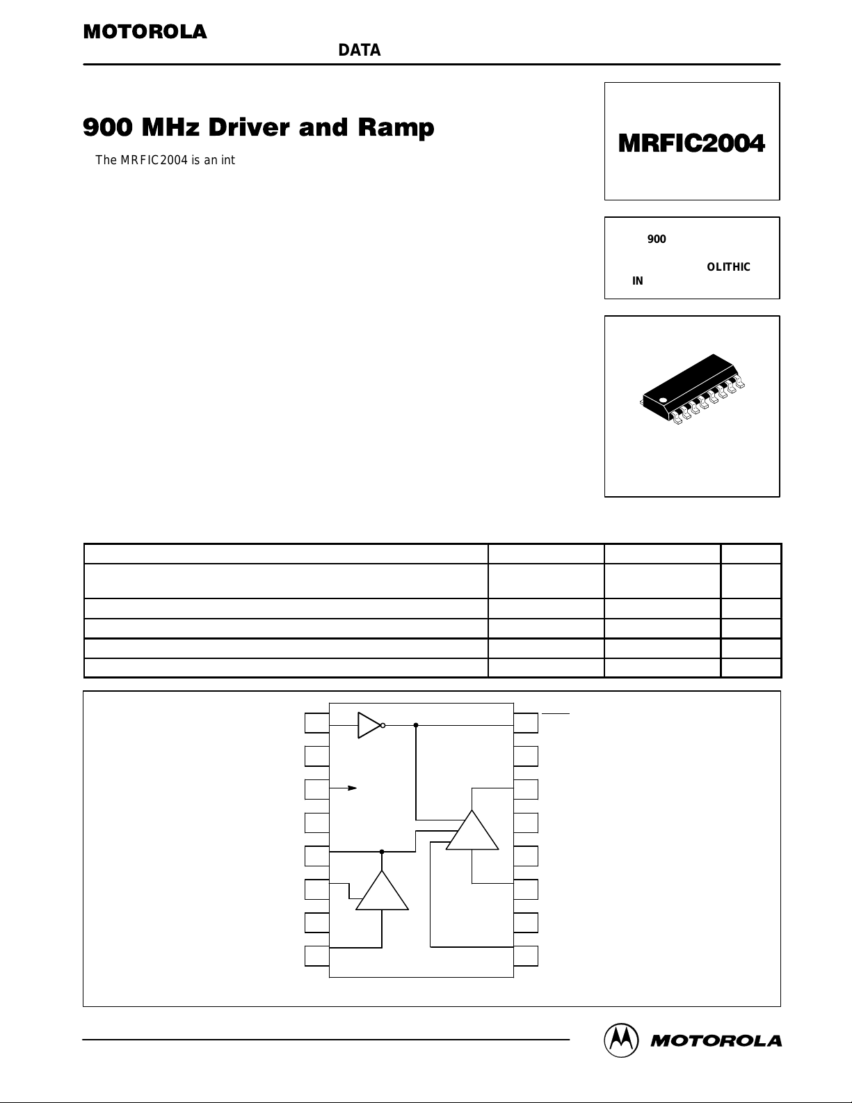
1RX EN
2
3
4
DRIVER
5
6
RAMP
7
RX EN
16
GND
15
RF OUT/V
14
GND
13
GND
12
RF IN
11
GND
10
cont
CC2
4.5
6.0
6.0 Vdc
+10 dBm
–35 to +85 °C
–65 to +150 °C
Vdc
REV 2
Motorola, Inc. 1997
TX EN
8
9
Pin Connections and Functional Block Diagram
V
cont
(GAIN CONTROL)
MRFIC2004MOTOROLA RF DEVICE DATA
1
Page 2
RECOMMENDED OPERATING RANGES
Parameter Symbol Value Unit
Supply Voltage Ranges V
Control Voltage Ranges TX EN, RX EN,
Frequency Range f 800 to 1000 MHz
ELECTRICAL CHARACTERISTICS (V
Characteristics (1)
Supply Current, TX EN High, RX EN Low — 11 13 mA
Supply Current, TX EN Low, RX EN High — 0.7 1.5 mA
Driver Characteristics (1)
Gain (Small Signal) 19 21.5 24 dB
Gain Control (Small Signal) — 34 — dB
Power Out @ 1.0 dB Gain Compression –4.0 –1.0 — dBm
Third Order Intercept Point (out) — +7.5 — dBm
Reverse Isolation — 32 — dB
Ramp Characteristics (1)
Ramp Up Delay Time
Rise Time
Total Time
Ramp Down Delay Time
Fall Time
Total Time
LOGIC LEVELS (V
High
Low
High
Low
NOTE:
1. All electrical characteristics measured in test circuit schematic shown in Figure 1 below.
= 2.7 to 4.0 V, TA = 25°C)
CC1
RX EN & TX EN Input Voltage
RX EN Output Voltage
CC1
, V
CC2
= 3.0 V, C
= 2.0 nF, TA = 25°C, f = 900 MHz, V
INT
V
V
, V
CC1
CC2
V
cont
Min Typ Max Unit
—
—
—
—
—
—
Min Typ Max Unit
– 0.8
CC1
—
– 0.2
CC1
—
4.0
18
22
4.0
18
22
—
—
—
—
2.7 to 4.0 Vdc
0 to V
CC1
= 1.3 V)
CONT
—
—
—
—
—
—
—
0.8
—
0.2
Vdc
µs
µs
V
V
MRFIC2004
2
MOTOROLA RF DEVICE DATA
Page 3
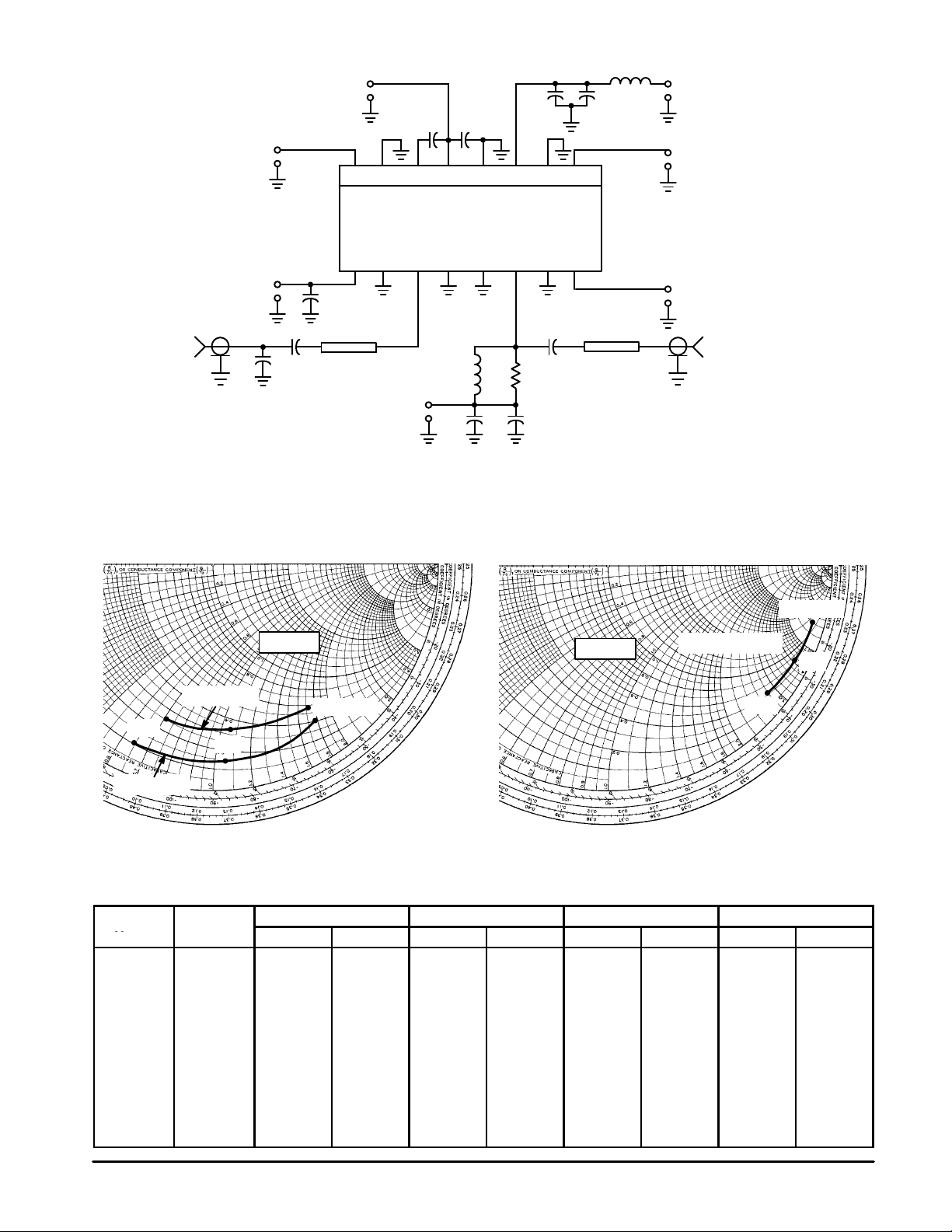
TX EN
f
V
cont
+
V
RAMP
–
C
C6
INT
+
–
D.U.T.
+
–
C9
C5 C7
12345678
161514131211109
L2
+
VCC 1
–
+
RX EN
–
+
RX EN
–
Ω
LINE
RF IN
50
Ω
C1, C7, C9 — 1000 pF Chip Capacitor
C2, C5, C6, C10 — 100 pF Chip Capacitor
C3 — 1.6 pF Chip Capacitor
C
— 2000 pF Chip Capacitor
INT
50
C10C11
Figure 1. T ypical Biasing Configuration
Zo = 50
Ω
V
= 1.0 V
cont
1000
750
f = 500 MHz
L1 R1
+
VCC 2
–
C11 — 6.2 pF Chip Capacitor
L1 — 4.7 nH Chip Inductor
L2 — 150 nH Chip Inductor
R1 — 330 Ω Chip Resistor
C3
C2C1
Ω
LINE
50
RF Connectors — SMA Type
Board Material — Epoxy/Glass εr= 4.5,
Dielectric Thickness = 0.014″ (0.36 mm)
Zo = 50
Ω
RF OUT
50
V
= 1.0 or 3.0 V
cont
Ω
f = 500 MHz
1000
750
V
= 3.0 V
cont
Figure 2. S11 versus Frequency versus V
S
f
V
cont
1.0 100 0.85 –11.3 10.48 –171.5 0.0002 142.7 0.99 –2.9
(MHz)
300 0.83 –32.8 10.33 –156.3 0.0020 129.0 0.99 –7.3
500 0.79 –56.9 10.15 –140.5 0.0030 130.6 0.98 –15.9
550 0.79 –62.5 10.04 –135.9 0.0030 132.6 0.98 –17.9
600 0.78 –68.5 9.85 –130.2 0.0040 133.3 0.98 –20.0
650 0.77 –74 9.47 –126.9 0.0040 135.9 0.98 –22.3
700 0.76 –79 9.23 –123.6 0.0050 137.2 0.98 –24.7
750 0.76 –84.4 9.02 –119.4 0.0050 138.1 0.97 –27.0
800 0.75 –89.6 8.69 –113.8 0.0060 139.7 0.97 –29.3
850 0.74 –94.5 8.33 –110.8 0.0070 140.3 0.97 –31.4
900 0.73 –99.1 8.13 –108.9 0.0080 141.2 0.96 –33.2
950 0.73 –102 7.98 –105.4 0.0090 138.3 0.96 –36.3
|S11| ∠φ |S21| ∠φ |S12| ∠φ |S22| ∠φ
11
cont
S
21
Figure 3. S22 versus Frequency
S
12
S
22
MRFIC2004MOTOROLA RF DEVICE DATA
3
Page 4

1000 0.72 –106.9 7.70 –101.0 0.0100 133.7 0.95 –38.4
1.9 100 0.85 –11.3 0.53 –173.5 0.0002 104.3 0.99 –2.9
300 0.86 –33.5 0.69 –169.7 0.0009 118.7 0.98 –8.7
500 0.87 –59.3 0.89 –179.5 0.0010 134.3 0.98 –15.5
550 0.87 –65.7 0.96 –175.1 0.0020 136.3 0.98 –17.5
600 0.88 –73.1 1.02 –169.9 0.0020 138.9 0.97 –19.6
650 0.88 –78.7 1.04 –167.3 0.0020 142.6 0.97 –21.8
700 0.88 –84.7 1.07 –165.0 0.0030 147.8 0.97 –24.1
750 0.89 –90.7 1.14 –161.5 0.0030 153.4 0.96 –26.4
800 0.89 –98.2 1.17 –155.8 0.0040 161.0 0.96 –28.8
850 0.88 –104.6 1.22 –151.2 0.0050 161.8 0.96 –30.7
900 0.87 –110.1 1.24 –144.6 0.0060 162.7 0.95 –32.8
950 0.86 –114.6 1.26 –139.9 0.0070 160.3 0.95 –35.1
1000 0.85 –118.8 1.27 –134.1 0.0080 158.2 0.94 –37.2
3.0 100 0.85 –10.9 0.003 –85.9 0.0001 115.0 0.99 –2.8
300 0.86 –31.9 0.014 –78.8 0.0006 121.0 0.99 –8.5
500 0.87 –56.9 0.032 –61.1 0.0010 128.0 0.98 –15.1
550 0.88 –62.4 0.038 –65.8 0.0010 136.2 0.98 –17.0
600 0.89 –69.4 0.048 –68.3 0.0010 140.0 0.98 –19.2
650 0.90 –75.1 0.058 –75.1 0.0020 145.1 0.98 –21.3
700 0.90 –81.3 0.069 –82.4 0.0020 150.8 0.97 –23.6
750 0.91 –87.3 0.081 –89.4 0.0020 156.8 0.97 –25.8
800 0.91 –93.8 0.092 –113.4 0.0030 160.3 0.97 –28.1
850 0.92 –100.7 0.092 –121.8 0.0040 163.3 0.96 –30.1
900 0.91 –106.8 0.089 –128.2 0.0050 163.3 0.96 –32.3
950 0.90 –111.4 0.083 –137.1 0.0060 155.2 0.95 –34.5
1000 0.89 –115.2 0.077 –151.9 0.0060 150.0 0.95 –36.6
T able 1. Small Signal Deembedded S Parameters
MRFIC2004
4
MOTOROLA RF DEVICE DATA
Page 5

24
18
12
6
0
–6
G, GAIN (dB)
–12
–18
–24
V
= 1 V
cont
1.9 V
TA = 25°C
V
3 V
f, FREQUENCY (MHz)
CC1
, V
CC2
= 3 V
1000900800700600500
6
3
0
–3
out
P , OUTPUT POWER (dBm)
–6
–9
–30
25°C
TA = –35°C
85°C
–26 – 22 –18 –14 –1
Pin, INPUT POWER (dBm)
Figure 4. Small Signal Gain versus Frequency Figure 5. Output Power versus Input Power
V
V
CC1
cont
, V
CC2
= 1 V
= 3 V
0
24
16
6
0
G, GAIN (dB)
–8
TA = 25°C
V
CC1
–16
1
–10 dBm
Pin = –30 dBm
, V
= 3 V
CC2
1.4 1.8 2.2 2.6 3
V
, GAIN CONTROL VOLTAGE (V)
cont
–20 dBm
–15 dBm
13
12
11
10
9
, SUPPLY CURRENT (mA)
C
I
8
7
–35
–15 5 25 45 65 85
TA, AMBIENT TEMPERATURE (
Figure 6. Driver Gain versus Gain Control Voltage Figure 7. Supply Current versus Ambient
Temperature
3
2.5
2
1.5
, RAMP VOLTAGE (V)
1
RAMP
V
0.5
0
0
TXEN LOW @ 50 µs
TA = 25°C
V
, V
CC2
= 2 nF
= 3 V
CC1
C
INT
DRIVER & PA
TURN ON
TXEN HIGH @ 10 µs
20 6040 80 100
tr & tf, RISE AND FALL TIME (
DRIVER & PA
TURN OFF
µ
s)
V
, V
CC1
CC2
TX EN HIGH
RX EN LOW
°
C)
= 3 V
Figure 8. Ramp V oltage versus Rise & Fall Time
MRFIC2004MOTOROLA RF DEVICE DATA
5
Page 6

APPLICATIONS INFORMATION
DESIGN PHILOSOPHY
The MRFIC2004 was designed as a support IC for a CT2
chip-set. The other chips making up the chip-set are the
MRFIC2001 downconverter, the MRFIC2002 transmit mixer,
the MRFIC2003 antenna switch and the MRFIC2006 PA. A
complete CT2 front-end solution requires a ramp for burst
control, an inverter for complementary antenna switch control and gain control (or an attenuator) for the transmitter low
power mode. In order to keep the other chips in the chip-set
relatively general purpose, yet provide the system designer
with an easily controlled solution, these functions were combined with a driver amplifier into one IC, the MRFIC2004.
THEORY OF OPERATION
The driver is a cascode design that exits the IC opencollector. Impedance matching must be done externally.
Since the output requires a bias inductor and DC blocking
capacitor, the output can be matched with these two elements. To keep the driver unconditionally stable, it is recommended that a 300 – 400 ohm resistor be placed in parallel
with the bias inductor as close to the IC as possible. Since
the output impedance of the driver by itself is very high, the
resistor sets the output impedance. The input can be
matched with a series inductor followed by a shunt capacitor.
Alternatively, a series transmission line followed by a shunt
capacitor can be used. A DC block is also required on the
input.
Gain control is provided to meet the CT2 low power
mode requirement. The CT2 Common Air Interface specification requires the transmitter to be capable of dropping
the output power by 16 ± 4.0 dB. Although the driver has
34 dB of small signal gain control, it can be reduced by ad-
ding a resistor in series with the gain control pin. The value
of the resistor depends on the logic levels being used and
the amount of gain compression after the driver. Also, the
amount of gain control is a function of the driver input power
level. The input power should be kept less than –10 dBm to
allow for sufficient gain control to achieve the low power
mode. The gain control can also be used for P A output power
trimming. However, this is not an efficient method.
The ramp is an integrator which is used to slow down the
driver and PA turn-on and turn-off times to reduce AM splatter. By applying a pulse waveform to the input, a linear ramp
waveform is created at the output which is then applied to the
current mirrors of the driver and PA. An external integrating
capacitor is used so that the rise/fall time can be programmed externally. A minimum value of 2.0 –2.4 nF is
needed to meet the CT2 Common Air Interface splatter specification. For non-TDD/TDMA systems the ramp reverts to an
enable/disable function.
The inverter is CMOS/TTL compatible and was included to
provide complementary control for an antenna switch such
as the MRFIC2003. By applying the receiver enable control
line, RXEN, to the inverter the inverse RXEN
RXEN and RXEN can then be used to control the
MRFIC2003 antenna switch.
EVALUATION BOARDS
Evaluation boards are available for RF Monolithic Integrated Circuits by adding a “TF” suffix to the device type.
For a complete list of currently available boards and ones
in development for newly introduced product, please con tact your local Motorola Distributor or Sales Office.
will be created.
MRFIC2004
6
MOTOROLA RF DEVICE DATA
Page 7

P ACKAGE DIMENSIONS
–T–
–A–
16 9
–B–
18
8 PLP
0.25 (0.010) B
G
K
C
SEATING
PLANE
D
16 PL
0.25 (0.010) A
M
S
B
T
M
S
CASE 751B–05
M
R
X 45
_
ISSUE J
NOTES:
1. DIMENSIONING AND TOLERANCING PER ANSI
Y14.5M, 1982.
2. CONTROLLING DIMENSION: MILLIMETER.
3. DIMENSIONS A AND B DO NOT INCLUDE
MOLD PROTRUSION.
4. MAXIMUM MOLD PROTRUSION 0.15 (0.006)
PER SIDE.
S
F
J
5. DIMENSION D DOES NOT INCLUDE DAMBAR
PROTRUSION. ALLOWABLE DAMBAR
PROTRUSION SHALL BE 0.127 (0.005) TOTAL
IN EXCESS OF THE D DIMENSION AT
MAXIMUM MATERIAL CONDITION.
DIM MIN MAX MIN MAX
A 9.80 10.00 0.386 0.393
B 3.80 4.00 0.150 0.157
C 1.35 1.75 0.054 0.068
D 0.35 0.49 0.014 0.019
F 0.40 1.25 0.016 0.049
G 1.27 BSC 0.050 BSC
J 0.19 0.25 0.008 0.009
K 0.10 0.25 0.004 0.009
M 0 7 0 7
____
P 5.80 6.20 0.229 0.244
R 0.25 0.50 0.010 0.019
INCHESMILLIMETERS
Motorola reserves the right to make changes without further notice to any products herein. Motorola makes no warranty , representation or guarantee regarding
the suitability of its products for any particular purpose, nor does Motorola assume any liability arising out of the application or use of any product or circuit, and
specifically disclaims any and all liability, including without limitation consequential or incidental damages. “T ypical” parameters which may be provided in Motorola
data sheets and/or specifications can and do vary in different applications and actual performance may vary over time. All operating parameters, including “Typicals”
must be validated for each customer application by customer’s technical experts. Motorola does not convey any license under its patent rights nor the rights of
others. Motorola products are not designed, intended, or authorized for use as components in systems intended for surgical implant into the body, or other
applications intended to support or sustain life, or for any other application in which the failure of the Motorola product could create a situation where personal injury
or death may occur. Should Buyer purchase or use Motorola products for any such unintended or unauthorized application, Buyer shall indemnify and hold Motorola
and its officers, employees, subsidiaries, affiliates, and distributors harmless against all claims, costs, damages, and expenses, and reasonable attorney fees
arising out of, directly or indirectly, any claim of personal injury or death associated with such unintended or unauthorized use, even if such claim alleges that
Motorola was negligent regarding the design or manufacture of the part. Motorola and are registered trademarks of Motorola, Inc. Motorola, Inc. is an Equal
Opportunity/Affirmative Action Employer.
Mfax is a trademark of Motorola, Inc.
How to reach us:
USA/EUROPE/Locations Not Listed: Motorola Literature Distribution; JAPAN: Nippon Motorola Ltd.: SPD, Strategic Planning Office, 4–32–1,
P.O. Box 5405, Denver, Colorado 80217. 303–675–2140 or 1–800–441–2447 Nishi–Gotanda, Shinagawa–ku, Tokyo 141, Japan. 81–3–5487–8488
Mfax: RMFAX0@email.sps.mot.com – TOUCHTONE 602–244–6609 ASIA/PACIFIC: Motorola Semiconductors H.K. Ltd.; 8B Tai Ping Industrial Park,
– US & Canada ONLY 1–800–774–1848 51 Ting Kok Road, T ai Po, N.T., Hong Kong. 852–26629298
INTERNET: http://motorola.com/sps
MRFIC2004/D
◊
MRFIC2004MOTOROLA RF DEVICE DATA
7
 Loading...