

Page 1
SEMICONDUCTOR TECHNICAL DATA
The MRFIC Line
The MRFIC2002 is a double-balanced, active mixer designed for transmitters
operating in the 800 MHz to 1.0 GHz frequency range. The design utilizes
Motorola’s advanced MOSAIC 3 silicon bipolar RF process to yield superior
performance in a cost effective monolithic device. Applications for the
MRFIC2002 include CT1 and CT2 cordless telephones, GSM, remote controls,
video and audio short range links, low cost cellular radios, and ISM band
transmitters. A power down control is provided to minimize current drain with
minimum recovery/turn-on time.
• Conversion Gain = 10 dB (Typ)
• Supply Current = 5.5 mA (Typ)
• Power Down Supply Current = 2.0 µA (Max)
• LO-RF Isolation = 25 dB (Typ)
• Low LO Drive Required = –10 dBm (Typ)
• LO Impedance Insensitive to Power Down
• No Matching Required for RF OUT Port
• All Ports are Single Ended
• Order MRFIC2002R2 for Tape and Reel.
R2 Suffix = 2,500 Units per 12 mm, 13 inch Reel.
• Device Marking = M2002
Order this document
by MRFIC2002/D
900 MHz TX-MIXER
SILICON MONOLITHIC
INTEGRATED CIRCUIT
CASE 751-05
(SO-8)
ABSOLUTE MAXIMUM RATINGS
Supply Voltage V
Control Voltages ENABLE, V
Input Power, LO and IF Ports PLO, P
Operating Ambient Temperature T
Storage Temperature T
(TA = 25°C unless otherwise noted)
Rating Symbol Value Unit
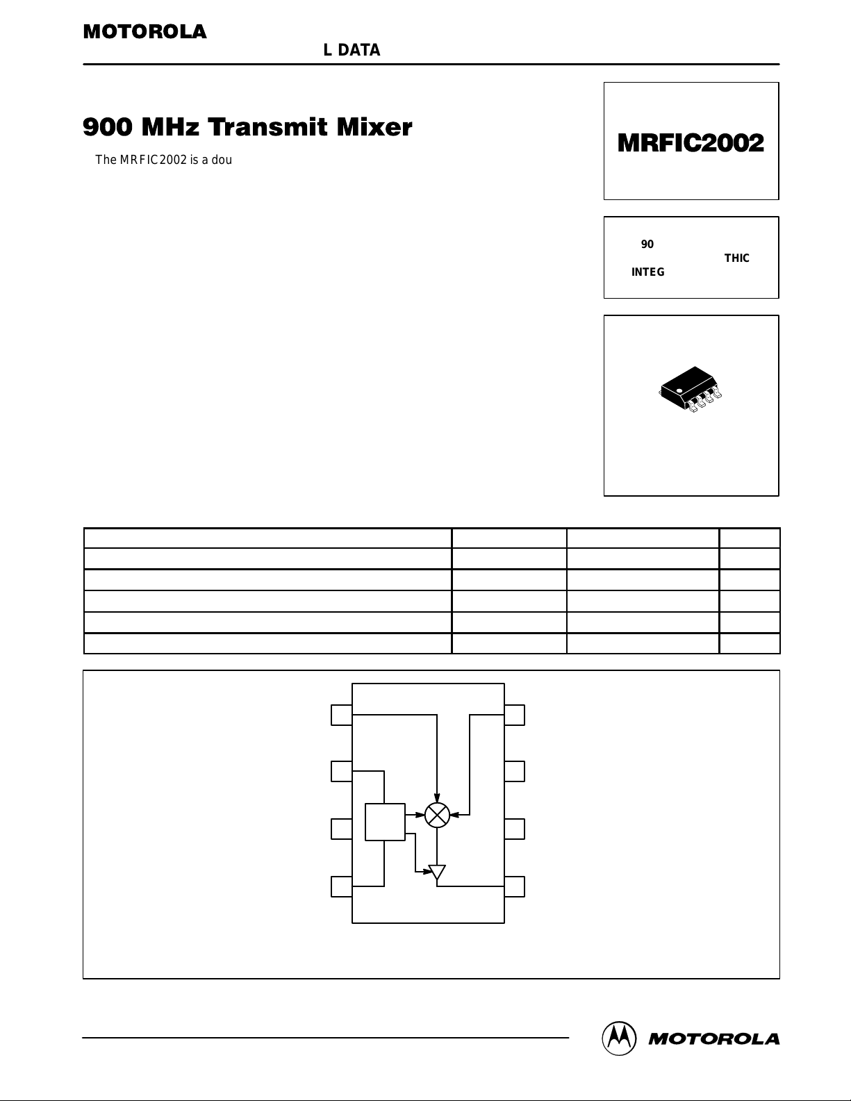
IF IN
1 8
(1)
V
RAMP
ENABLE
2 7
GND
BIAS
3 6
CNTL
4 5
CC
A
stg
RAMP
IF
LO IN
V
CC
GND
RF OUT
5.5 Vdc
5.0 Vdc
+10 dBm
–35 to +85 °C
–65 to +150 °C
REV 2
Motorola, Inc. 1997
(1) For CT2 applications, apply ramp voltage provided in MRFIC2004. For non-CT2, leave open circuited.
Pin Connections and Functional Block Diagram
MRFIC2002MOTOROLA RF DEVICE DATA
1
Page 2
RECOMMENDED OPERATING RANGES
Parameter Symbol Value Unit
Supply Voltage Range V
Control Voltage Ranges ENABLE, V
RF Port Frequency Range f
IF Port Frequency Range f
ELECTRICAL CHARACTERISTICS (V
GHz, RF @ 900 MHz, TA = 25°C unless otherwise noted)
Characteristic (2)
Supply Current: On-Mode
Supply Current: Off-Mode (Enable < 1.0 V)
Enable Response Time — 1.0 — µs
Conversion Gain 8.0 10 12 dB
Single Sideband Noise Figure — 10 — dB
Output Power at 1.0 dB Gain Compression — –18 — dBm
Output Power at Saturation –16 –14 — dBm
LO-RF Isolation (1.0 GHz) — 25 — dB
LO-IF Isolation (1.0 GHz) — 65 — dB
IF-RF Isolation (100 MHz) — 18 — dB
IF-LO Isolation (100 MHz) — 50 — dB
NOTES:
1. For CT2 applications, apply ramp voltage provided in MRFIC2004. For non-CT2, leave open circuited.
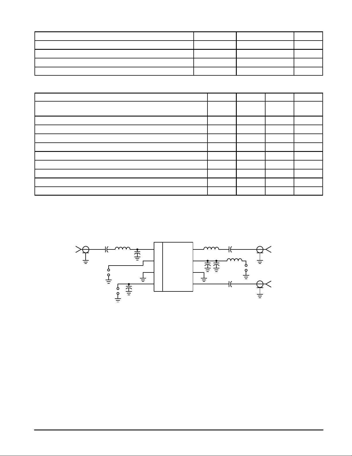
2. All Electrical Characteristics are measured in test circuit schematic as shown in Figure 1.
, Enable = 3.0 V and V
CC
Ramp
(1)
Open Circuited, PLO = –7.0 dBm, IF @ 100 MHz, LO @ 1.0
CC
RAMP
RF
IF
Min Typ Max Unit
—
—
2.7 to 5.0 Vdc
0 to 5.0 Vdc
500 to 1000 MHz
0 (dc) to 250 MHz
5.5
0.1
7.0
2.0
mA
µA
IF IN
Ω
50
C1 L1 L2
C2
V
+
*
RAMP
–
ENABLE
C1, C3, C6 — 1000 pF Chip Capacitor
C2 — 6.8 pF Chip Capacitor
C4 — 3.9 pF Chip Capacitor
C5 — 100 pF Chip Capacitor
C7 — 5.6 pF Chip Capacitor
L1 — 270 nH Chip Inductor
+
–
C3
1
2
3
4
8
7
D.U.T.
6
5
L2 — 10 nH Chip Inductor
L3 — 390 nH Chip Inductor
RF Connectors — SMA Type
Board Material — Glass/Epoxy εr = 4.5,
Dielectric Thickness = 0.014″ (0.36 mm)
Figure 1. T est Circuit
Configuration
C4
L3
C6C5
C7
+
–V
CC
LO IN
50
Ω
RF OUT
50
Ω
MRFIC2002
2
MOTOROLA RF DEVICE DATA
Page 3

13
12
11
TA = –35°C
+25°C
f = 0.5 GHz
Z
RF
Zo = 50
Ω
0.9
1.2
1.2
Z
LO
f = 0.5 GHz
0.7
0.9
0
Z
IF
0.1
f = 0.25 GHz
10
, CONVERSION GAIN (dB)
C
G
9
8
fRF, RF FREQUENCY (MHz)
Figure 3. Gain versus RF Frequency
18
16
14
12
, CONVERSION GAIN (dB)
C
G
10
8
fRF, RF FREQUENCY (MHz)
VCC = 5 V
4 V
3 V
+85°C
VCC = 3 V
fIF = 100 MHz
TA = 25°C
fIF = 100 MHz
900600500 700 800
900600500 700 800 1000
1000
Figure 2. Port Impedances versus Frequency
Γ
IF
V
CC
(Volts)
3.0 50 0.83 –2.4 — — — —
f
(MHz)
100 0.82 –4.7 — — — —
150 0.82 –7.1 — — — —
200 0.81 –9.6 — — — —
250 0.81 –11.7 — — — —
500 — — 0.42 100 0.57 –29
600 — — 0.41 94 0.55 –35
700 — — 0.40 88 0.54 –41
800 — — 0.39 80 0.52 –48
900 — — 0.36 71 0.51 –54
1000 — — 0.33 63 0.50 –60
1100 — — 0.31 55 0.49 –65
1200 — — 0.28 45 0.49 –70
Mag
∠φ
Degrees
Figure 4. Gain versus RF Frequency
Γ
RF
∠φ
Mag
Degrees
Mag
Γ
LO
T able 1. Deembedded Port Reflection Coefficients
(Enable = 3.0 V, Zo = 50 Ω, TA = 25°C)
∠φ
Degrees
MRFIC2002MOTOROLA RF DEVICE DATA
3
Page 4

11
10
TA = –35°C
25°C
16
14
VCC = 5 V
4 V
9
, CONVERSION GAIN (dB)
8
C
G
7
–12–15 0
PLO, LO INPUT POWER (dBm)
Figure 5. Gain versus LO Input Power
–12
–14
–16
TA = –35°C
–18
25°C
RF
P , OUTPUT POWER (dBm)
–20
–22
–30
85°C
–26 – 22 –18 –14 –10
PIF, IF INPUT POWER (dBm)
85°C
VCC = 3 V
–9 –3
–6
VCC = 3 V
12
, CONVERSION GAIN (dB)
10
C
G
8
–12–15 0–6–9 –3
PLO, LO INPUT POWER (dBm)
3 V
TA = 25°C
Figure 6. Gain versus LO Input Power
–2
–
ā
6
–10
–14
RF
P , OUTPUT POWER (dBm)
–18
–
ā
22
–30 –26 – 22 –18 –14 –10
VCC = 5 V
3 V
PIF, IF INPUT POWER (dBm)
4 V
TA = 25°C
Figure 7. Output Power versus IF Input Power Figure 8. Output Power versus IF Input Power
–
ā
8
VCC = 5 V
–10
–12
–14
, OUTPUT POWER (dBm)
–16
o 1.0 dB
P
–18
3 V
PLO, LO INPUT POWER (dBm)
4 V
TA = 25°C
ā
6
ā
3–12–15 –ā9–
–
0
Figure 9. Output Power at 1.0 dB Gain Compression
versus LO Input Power
MRFIC2002
4
MOTOROLA RF DEVICE DATA
Page 5

14
12
10
8
, SUPPLY CURRENT (mA)
CC
I
6
TA = +ā85°C
–ā35°C
25°C
8
6
4
, SUPPLY CURRENT (mA)
2
CC
I
25°C
T
= 85°C
A
–ā35°C
VCC = 3 V
4
3.43 5
3.8 4.6
VCC, SUPPLY VOLTAGE (V)
Figure 10. ICC versus V
4.2
CC
APPLICATIONS INFORMATION
DESIGN PHILOSOPHY
The MRFIC2002 was designed to have excellent LO and
spurious rejection. This is accomplished by using a doublebalanced configuration and using a symmetrical die layout.
To eliminate the need for external baluns or decoupling
elements, the unused LO and IF ports are decoupled internally. Only one of the RF outputs is used, eliminating the
need for an external balun on the RF port as well. Also, the
RF port is buffered to provide a 50 ohm output impedance.
External matching is required for the LO and IF ports.
To minimize current drain in various TDD/TDMA systems,
two methods of enabling/disabling the MRFIC2002 are provided: one that is TTL/CMOS compatible and one that is triggered from a ramp, such as the one provided in the
MRFIC2004. The former method must be used if a ramp is
not available. The latter method is more desirable since the
MRFIC2002 can remain off during guard times and while in
idle mode.
THEORY OF OPERATION
Matching the LO port to 50 ohms can be done several
ways. The recommended approach is a series inductor as
close to the IC as possible. The inductor value is small
enough (~8 –15 nH depending on LO frequency) to be
printed on the board. A DC block is required and should not
be placed between the inductor and IC since this will prevent
the inductor from being placed close enough to the IC to provide a good match.
The IF port is approximately 500 ohms resistive in parallel
with 1.3 pF of capacitance. If 50 ohms is the desired IF port
impedance, a shunt capacitor followed by a series inductor
0
10 5324
VEN, ENABLE VOLTAGE (V)
Figure 11. ICC versus Enable V oltage
will provide the transformation. A DC block is required and
can be placed on either side of the matching network.
The RF port is nearly 50 ohms resistive in series with a
small amount of inductive reactance, which results in an
8 –11 dB return loss. However, a series 5.6 pF capacitor
placed as close to the IC as possible will typically provide
greater than a 15 dB return loss. The series capacitor also
serves as a DC block which is required.
Supply decoupling must be done as close to the IC as possible. A 1000 pF capacitor is recommended. An additional
100 pF capacitor and an RF choke are recommended to
keep the RF and LO signals off the supply line.
For systems that use a ramp, like the one provided in the
MRFIC2004, enabling/disabling can be done by applying the
ramp voltage to the V
pin which trips the IC between
RAMP
0.6 and 1.0 volts. The Enable pin must either be tied high or
to the inverse of the receiver enable control line, RXEN
. An
inverter is provided in the MRFIC2004 to invert RXEN.
For systems that do not use a ramp, the V
RAMP
pin can
be left open circuited and enabling/disabling the MRFIC2002
can be done with its TTL/CMOS compatible Enable pin. The
trip point is between 1.0 and 2.0 volts.
EVALUATION BOARDS
Evaluation boards are av ailable for RF Monolithic Integrated Circuits by adding a “TF” suffix to the device type.
For a complete list of currently available boards and ones
in development for newly introduced product, please con tact your local Motorola Distributor or Sales Office.
MRFIC2002MOTOROLA RF DEVICE DATA
5
Page 6

P ACKAGE DIMENSIONS
A
E
B
C
A1
D
58
0.25MB
1
H
4
e
M
h
X 45
_
q
C
A
SEATING
PLANE
0.10
L
B
SS
A0.25MCB
NOTES:
1. DIMENSIONING AND TOLERANCING PER ASME
Y14.5M, 1994.
2. DIMENSIONS ARE IN MILLIMETERS.
3. DIMENSION D AND E DO NOT INCLUDE MOLD
PROTRUSION.
4. MAXIMUM MOLD PROTRUSION 0.15 PER SIDE.
5. DIMENSION B DOES NOT INCLUDE MOLD
PROTRUSION. ALLOWABLE DAMBAR
PROTRUSION SHALL BE 0.127 TOTAL IN EXCESS
OF THE B DIMENSION AT MAXIMUM MATERIAL
CONDITION.
MILLIMETERS
DIM MIN MAX
A 1.35 1.75
A1 0.10 0.25
B 0.35 0.49
C 0.18 0.25
D 4.80 5.00
E
3.80 4.00
1.27 BSCe
H 5.80 6.20
h
0.25 0.50
L 0.40 1.25
0 7
q
__
CASE 751–05
ISSUE S
Motorola reserves the right to make changes without further notice to any products herein. Motorola makes no warranty , representation or guarantee regarding
the suitability of its products for any particular purpose, nor does Motorola assume any liability arising out of the application or use of any product or circuit, and
specifically disclaims any and all liability, including without limitation consequential or incidental damages. “T ypical” parameters which may be provided in Motorola
data sheets and/or specifications can and do vary in different applications and actual performance may vary over time. All operating parameters, including “Typicals”
must be validated for each customer application by customer’s technical experts. Motorola does not convey any license under its patent rights nor the rights of
others. Motorola products are not designed, intended, or authorized for use as components in systems intended for surgical implant into the body, or other
applications intended to support or sustain life, or for any other application in which the failure of the Motorola product could create a situation where personal injury
or death may occur. Should Buyer purchase or use Motorola products for any such unintended or unauthorized application, Buyer shall indemnify and hold Motorola
and its officers, employees, subsidiaries, affiliates, and distributors harmless against all claims, costs, damages, and expenses, and reasonable attorney fees
arising out of, directly or indirectly, any claim of personal injury or death associated with such unintended or unauthorized use, even if such claim alleges that
Motorola was negligent regarding the design or manufacture of the part. Motorola and are registered trademarks of Motorola, Inc. Motorola, Inc. is an Equal
Opportunity/Affirmative Action Employer.
How to reach us:
USA/EUROPE/Locations Not Listed: Motorola Literature Distribution; JAPAN: Nippon Motorola Ltd.: SPD, Strategic Planning Office, 4–32–1,
P.O. Box 5405, Denver, Colorado 80217. 303–675–2140 or 1–800–441–2447 Nishi–Gotanda, Shinagawa–ku, Tokyo 141, Japan. 81–3–5487–8488
Mfax: RMFAX0@email.sps.mot.com – TOUCHTONE 602–244–6609 ASIA/PACIFIC: Motorola Semiconductors H.K. Ltd.; 8B Tai Ping Industrial Park,
INTERNET: http://motorola.com/sps
MRFIC2002
– US & Canada ONLY 1–800–774–1848 51 Ting Kok Road, T ai Po, N.T., Hong Kong. 852–26629298
◊
Mfax is a trademark of Motorola, Inc.
MOTOROLA RF DEVICE DATA
MRFIC2002/D
6
 Loading...