

Page 1
SEMICONDUCTOR TECHNICAL DATA
The MRFIC Line
!
Order this document
by MRFIC1817/D
Designed specifically for application in Pan European digital 1.0 watt
DCS1800/PCS1900 handheld radios, the MRFIC1817 is specified for 32 dBm
output power with power gain over 27 dB from a 3.6 volt supply . To achieve this
superior performance, Motorola’s planar GaAs MESFET process is employed.
The device is packaged in the PFP–16 Power Flat Package which gives
excellent thermal and electrical performance through a solderable backside
contact while allowing the convenience and cost benefits of reflow soldering.
• Minimum Output Power Capabilities
32 dBm @ 3.6 Volts
30 dBm @ 3.0 Volts
• Typical Volt Characteristics
RF Input Power = 5.0 dBm
RF Output Power = 33.5 dBm
Typical PAE = 42%
• Low Current required from Negative Supply – 2 mA max
• Guaranteed Stability and Ruggedness
• Order MRFIC1817R2 for Tape and Reel.
R2 Suffix = 1,500 Units per 16 mm, 13 inch Reel.
• Device Marking = M1817
ABSOLUTE MAXIMUM RATINGS
DC Positive Supply Voltage V
DC Negative Supply Voltage V
RF Input Power P
RF Output Power P
Operating Case Temperature Range T
Storage Temperature Range T
Thermal Resistance, Junction to Case R
(TA = 25°C, ZO = 50 Ω, unless otherwise noted)
Rating
Symbol Value Unit
D1, 2, 3
stg
θJC
SS
in
out
C
1700–1900 MHz MMIC
DCS1800/PCS1900
INTEGRATED POWER AMPLIFIER
GaAs MONOLITHIC
INTEGRATED CIRCUIT
CASE 978–02
(PFP–16)
6 Vdc
–5 Vdc
10 dBm
35 dBm
–35 to +85 °C
–55 to +150 °C
10 °C/W
Motorola, Inc. 1997
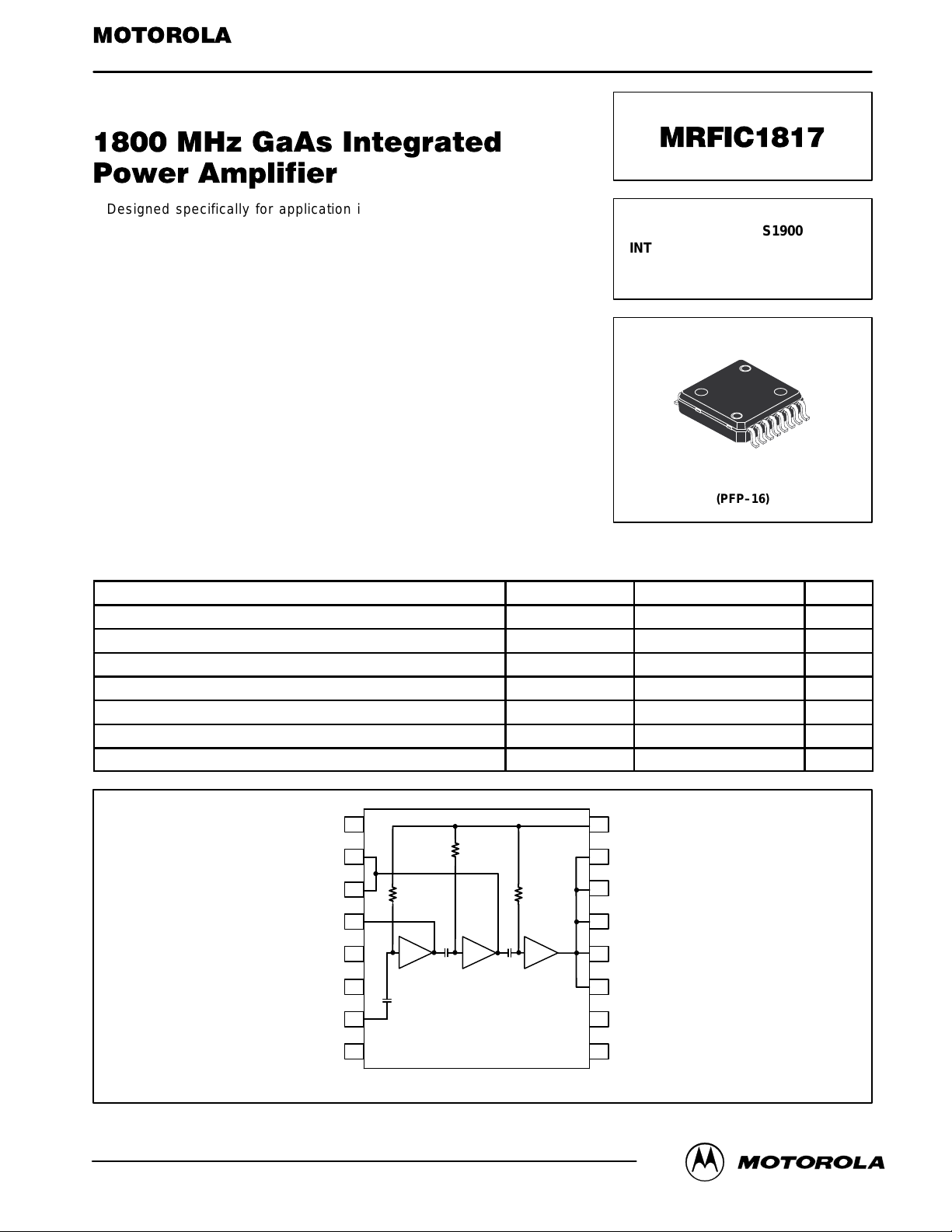
GND
V
D2
V
D2
V
D1
N/C
GND
RF IN
N/C
9
10
11
12
13
14
15
16
8
7
6
5
4
3
2
1
Pin Connections and Functional Block Diagram
V
G
V
D3
RF OUT
RF OUT
RF OUT
RF OUT
N/C
GND
MRFIC1817MOTOROLA RF DEVICE DATA
1
Page 2
RECOMMENDED OPERATING RANGES
Parameter Symbol Value Unit
Supply Voltage V
Gate Voltage V
RF Frequency Range f
RF Input Power P
D1, 2, 3
SS
RF
RF
2.7 to 5 Vdc
–3.5 to –4.5 Vdc
1700 to 1900 MHz
0 to 6 dBm
ELECTRICAL CHARACTERISTICS (V
= 3.6 V, VSS = –4 V, Pin = 5 dBm, Peak Measurement at 12.5% Duty Cycle, 4.6 ms
D1, 2, 3
Period, TA = 25°C unless otherwise noted. Measured in Reference Circuit Shown in Figure 1)
Characteristic
Min Typ Max Unit
Frequency Range 1710 — 1785 MHz
Output Power 32 33.5 — dBm
Power Added Efficiency 35 42 — %
Output Power (PCS 1900 Tuning f = 1850 to 1910 MHz) — 33.5 — dBm
Power Added Efficiency (PCS 1900 Tuning f = 1850 to 1910 MHz) — 42 — %
Input VSWR — 2:1 — VSWR
Harmonic Output (2nd and 3rd) — –35 –30 dBc
Output Power at Low voltage (VD1, VD2, VD3 = 3.0 V) 30 32 — dBm
Output Power Isolation (VD1, VD2, VD3 = 0 V) — –40 –30 dBm
Noise Power (In 100 kHz, 1805 to 1880 MHz) — –85 –80 dBm
Stability – Spurious Output (Pin = 5 dBm, P
VSWR = 6:1 at any Phase Angle, Source VSWR = 3:1, at any Phase Angle)
Load Mismatch stress (P
any Phase Angle)
= 33 dBm, Load VSWR = 10:1 at
out
(1)
= 0 to 33 dBm, Load
out
(1)
— — –60 dBc
No Degradation in Output Power after Returning to
Standard Conditions
3 dB VDD Bandwidth — 2 — MHz
Negative Supply Current — 0.7 2 mA
(1) Adjust V
(0 to 3.6 V) for specified P
D1, 2, 3
V
D1
; Duty Cycle = 12.5%, Period = 4.6 ms.
out
V
D2
V
V
D3
SS
9
T4
T3
NC
NC
10
11
12
13
14
15
16
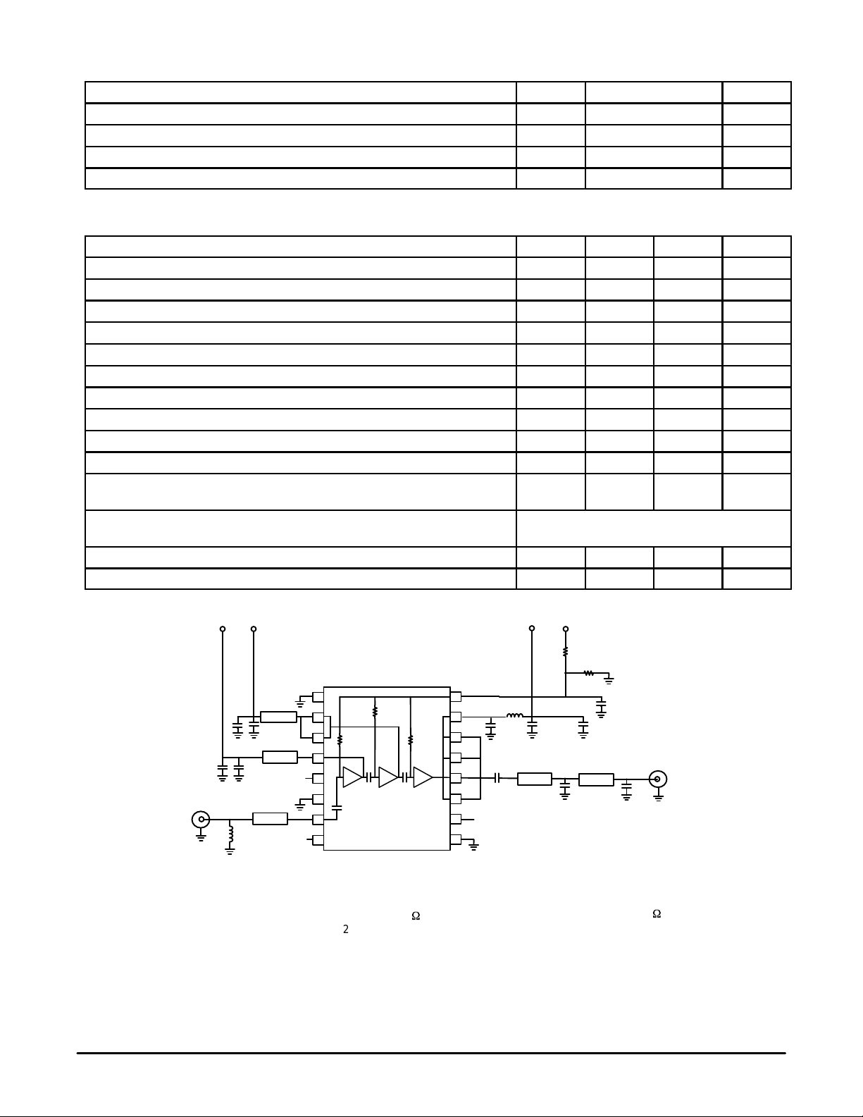
L1 18 nH, Coilcraft or 20 mm
50 Ω Microstrip Line
L2 1.8 nH, Toko 2012
R1 2.7 K
W
R2 2.2 KΩ
T1 2.5 mm 50 Ω Microstrip Line
C9 C8
C7 C6
T2
RF IN
L2
C1 1 nF
C2, C6, C8 22 pF, NPO/COG
C3, C7, C9 47 nF
C4 5.6 pF, AVX0603 ACCUF
C5 3.9 pF, AVX0603 ACCUF
C10, C11 1 pf
NOTE: For PCS 1900 tuning the following values are changed.
C5 = 2.7 pF, AVX0603 ACCUF
L2 = 1.5 nH, Toko 2012
T3 = 1 mm 50 Ω Microstrip Line
Figure 1. Reference Circuit Configuration
R1
R2
8
7
6
5
4
3
2
1
NC
C4
L1
C11
T1
C5
C1
C3C2
T5
RF
OUT
C10
T2 6 mm 50 Ω Microstrip Line
T3 5 mm 40 Ω Microstrip Line
T4 1 mm 40 Ω Microstrip Line
T5 5.5 mm 50 W Microstrip Line
ε
Board Material: Glass/Epoxy,
Thickness = 0.5 mm
= 4.45,
r
MRFIC1817
2
MOTOROLA RF DEVICE DATA
Page 3
0 V
0 V
C13
CR1
C15
C14
3.0 V
3.0 V
1
2
3
4
5
6
7
V
reg
VRAMP
STANDBY
U2
R4
RF IN
D
V
BAT
R3
14
13
C16
12
C17
11
10
9
8
C10
C12
C9
L2
C19
T2
T4
T3
C18
NC
NC
R5
C11
9
10
11
12
13
14
15
16
5
6
7
8
IN
G
4
D
S
3
D
S
2
D
1
Q1
R2R1
VG TUNE
8
7
6
5
4
3
2
1
C4
NC
C21
L1
T1
T5
C5
C1
C3C2
RF
OUT
C20
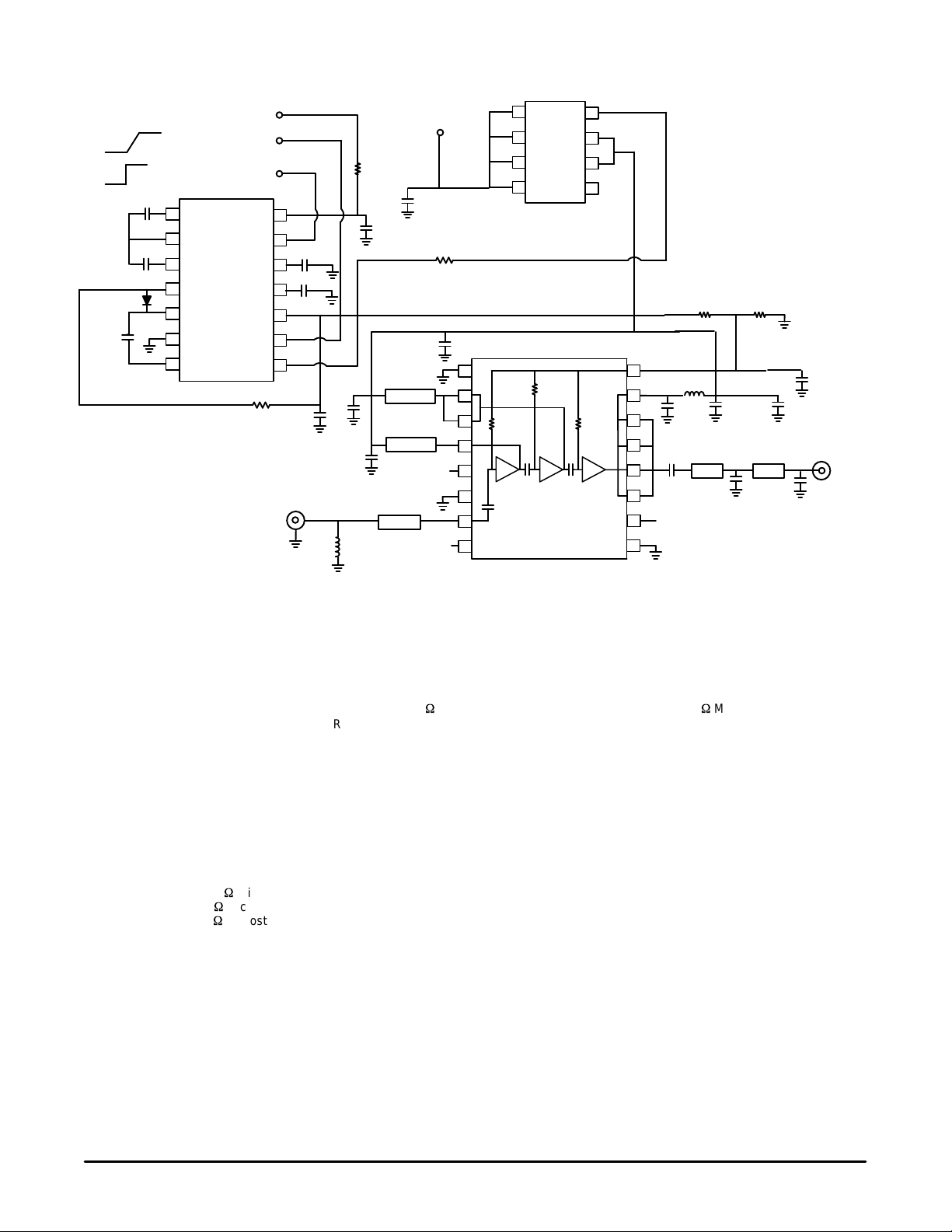
C1 6.8 nF
C2, C9, C10 22 pF, 0603 NPO/COG
C3, C11 47 nF
C20, C21 1 pF
CR1 MMBD701LT1
L1 18 nH, Coilcraft or 20 mm
C4 5.6 pF, AVX0603 ACCUF
C5 3.9 pF, AVX0603 ACCUF
C12 220 nF
C13, C16, C17, C19 1 µF
C14, C15 1 µF
C18 1 µF
L2 1.8 nH, Toko 2012
Q1 MMSF4N01HD
R1 2.7 K
R2 3 KΩ
R3 22 Ω
NOTE: For PCS1900 applications, the following
component values are changed
L2 = 1.5 nH Toko 2012
C4 = 6.8 pF, AVX0603 ACCUF
C5 = 2.7 pF, AVX0603 ACCUF
C20 = Not Used
T1 = 0.5 mm 50 W Microstrip Line
T2 = 5 mm 50 W Microstrip Line
T3 = 1 mm 40
Microstrip Line
Figure 2. DCS1800/PCS1900 Applications Circuit Configuration
50 Ω Microstrip Line
W
U1
R4 100 Ω
R5 470 Ω
T1 0.5 mm 30 Ω Microstrip Line
T2 5 mm 50 Ω Microstrip Line
T3 8 mm 50 Ω Microstrip Line
T4 1 mm 50 Ω Microstrip Line
T5 5.5 mm 50 W Microstrip Line
U1 MRFIC1817
U2 MC33169 (–4 V Version)
Board Material: Glass/Epoxy,
Thickness = 0.5 mm
ε
= 4.45,
r
MRFIC1817MOTOROLA RF DEVICE DATA
3
Page 4

T ypical Characteristics
33
32.5
32
31.5
31
out
P , OUTPUT POWER (dBm)
Pin = 5 dBm
30.5
VD1, V
VSS = –4 V
30
1.7 1.72 1.74 1.76 1.78 1.8
D2, VD3
= 3 V
f, FREQUENCY (GHz)
TA = –35°C
25°C
85°C
Figure 3. Output Power versus Frequency Figure 4. Power Added Efficiency
35
34.5
34
33.5
33
out
P , OUTPUT POWER (dBm)
32.5
Pin = 5 dBm
VD1, V
VSS = –4 V
32
1.7 1.72 1.74 1.76 1.78 1.8
D2, VD3
= 3.6 V
f, FREQUENCY (GHz)
TA = –35°C
25°C
85°C
48
TA = –35°C
46
44
42
40
38
PAE, POWER ADDED EFFICIENCY (%)
36
1.7 1.72 1.74 1.76 1.78 1.8
f, FREQUENCY (GHz)
25°C
85°C
Pin = 5 dBm
VD1, V
D2, VD3
VSS = –4 V
versus Frequency
46
45
44
43
42
41
40
PAE, POWER ADDED EFFICIENCY (%)
39
1.7 1.72 1.74 1.76 1.78 1.8
f, FREQUENCY (GHz)
VD1, VD2, VD3 = 4.2 V
3.6 V
3 V
Pin = 5 dBm
TA = 25
VSS = –4 V
= 3.6 V
°
C
Figure 5. Output Power versus Frequency Figure 6. Power Added Efficiency
36
35.5
35
34.5
34
out
P , OUTPUT POWER (dBm)
Pin = 5 dBm
33.5
VD1, V
VSS = –4 V
33
1.7 1.72 1.74 1.76 1.78 1.8
D2, VD3
= 4.2 V
f, FREQUENCY (GHz)
TA = –35°C
°
C
25
85°C
Figure 7. Output Power versus Frequency Figure 8. Output Power versus Drain Voltage
MRFIC1817
4
versus Frequency
40
TA = –35°C
30
20
10
–10
–20
–30
out
P , OUTPUT POWER (dBm)
–40
–50
–60
25°C AND 85°C
0
f = 1.75 GHz
Pin = 5 dBm
VSS = –4 V
01 345
V
D1
2
, VD2, VD3, DRAIN VOLTAGE (VOLTS)
MOTOROLA RF DEVICE DATA
Page 5

T ypical Characteristics
60
50
TA = –35°C
40
30
20
10
PAE, POWER ADDED EFFICIENCY (%)
0
01 345
85°C
V
, VD2, VD3, DRAIN VOLTAGE (VOLTS)
D1
25
°
C
f = 1.75 GHz
Pin = 5 dBm
VSS = –4 V
2
Figure 9. Power Added Efficiency versus
Drain Voltage
50
45
40
35
30
25
20
15
10
PAE, POWER ADDED EFFICIENCY (%)
5
0
–20 –15 –10 –5 0 10
TA = –35°C
25°C
85°C
Pin, INPUT POWER (dBm)
f = 1.75 GHz
VD1, V
VSS = –4 V
D2, VD3
= 3.6 V
5
Figure 11. Power Added Efficiency versus
Input Power
35
33
31
29
27
25
23
21
out
P , OUTPUT POWER (dBm)
19
17
15
–20 –15 –10 –5 0 10
TA = –35°C
25°C
85°C
Pin, INPUT POWER (dBm)
f = 1.75 GHz
VD1, V
D2, VD3
VSS = –4 V
= 3.6 V
5
Figure 10. Output Power versus Input Power
–20
–25
–30
–35
–40
–45
, SECOND HARMONIC (dBc)
–50
2
H
–55
–60
024
85°C
135
V
D1
TA = –35°C
25°C
, VD2, VD3, DRAIN VOLTAGE (VOLTS)
f = 1.75 GHz
Pin = 5 dBm
VSS = –4 V
Figure 12. Second Harmonic versus
Drain Voltage
0
–5
–10
–15
–20
–25
, THIRD HARMONIC (dBc)
3
–30
H
–35
–40
0245
25°C
13
V
, VD2, VD3, DRAIN VOLTAGE (VOLTS)
D1
TA = –35°C
f = 1.75 GHz
Pin = 5 dBm
VSS = –4 V
85°C
35
34.5
34
33.5
33
32.5
32
out
P , OUTPUT POWER (dBm)
31.5
31
Figure 13. Third Harmonic versus
Drain Voltage
TA = –35°C
25°C
85°C
Pin = 5 dBm
VD1, VD2, VD3 = 3.6 V
VSS = –4 V
1.85 1.86 1.88 1.89 1.9 1.91
1.87
f, FREQUENCY (GHz)
Figure 14. Output Power versus
Frequency – PCS Band
MRFIC1817MOTOROLA RF DEVICE DATA
5
Page 6

48
T ypical Characteristics
46
44
42
40
38
36
34
PAE, POWER ADDED EFFICIENCY (%)
32
1.85 1.86 1.88 1.89 1.9 1.91
TA = –35°C
25°C
85
°
C
1.87
f, FREQUENCY (GHz)
Figure 15. Power Added Efficiency versus
Frequency – PCS Band
T able 1. Optimum Loads Derived from
Circuit Characterization
Z
in
7.77
7.84
7.87
8.07
8.24
8.39
8.44
8.52
8.57
OHMS
jXRjXR
–34.15
–34.37
–34.67
–34.79
–35.05
–35.22
–35.56
–35.79
–35.82
f
MHz
1710
1720
1730
1740
1750
1760
1770
1780
1785
Zin represents the input impedance of the device.
ZOL* represents the conjugate of the optimum output load to present
to the device.
4.89
4.87
4.86
4.78
4.77
4.73
4.70
4.67
4.65
ZOL*
OHMS
9.50
9.34
9.18
8.94
8.70
8.51
8.32
8.12
7.95
Pin = 5 dBm
VD1, V
VSS = –4 V
D2, VD3
= 3.6 V
T able 2. Optimum Loads Derived from
Circuit Characterization – PCS Band
Z
in
3.97
3.94
4.09
4.04
4.18
4.27
4.26
OHMS
jXRjXR
–39.68
–40.31
–40.65
–40.92
–41.21
–41.48
–41.71
f
MHz
1850
1860
1870
1880
1890
1900
1910
Zin represents the input impedance of the device.
ZOL* represents the conjugate of the optimum output load to present
to the device.
7.49
7.42
7.38
7.31
7.28
7.28
7.23
ZOL*
OHMS
3.07
2.81
2.51
2.28
2.02
1.73
1.56
MRFIC1817
6
MOTOROLA RF DEVICE DATA
Page 7

APPLICATIONS INFORMATION
Design Philosophy
The MRFIC1817 is a 3–stage integrated power amplifier
designed for use in cellular phones, especially for those used
in DCS1800 (PCN) 3.6 V operation. With matching circuit
modifications, it is also applicable for use in DCS1900 (PCS)
equipment. Due to the fact that the input, output and some of
the interstage matching is accomplished off–chip, the device
can be tuned to operate anywhere within the 1500 to 2000
MHz frequency range. Typical performance at dif ferent battery
voltages is:
• 33.5 dBm @ 3.6 V
• 32.0 dBm @ 3 V
This capability makes the MRFIC1817 suitable for portable
cellular applications such as:
• 3 V and 3.6 V DCS1800 Class I and II
• 3 V and 3.6 V PCS tag5
RF Circuit Considerations
The MRFIC1817 can be tuned by changing the values
and/or positions of the appropriate external components.
Refer to Figure 2, a typical DCS1800 Class I applications
circuit. The input match is a shunt–L, series–C, high–pass
structure and can be retuned as desired with the only
limitation being the on–chip 6 pF blocking capacitor. For
saturated applications such as DCS1800 and PCS1900, the
input match should be optimized at the rated RF input power.
Interstage matching can be optimized by changing the value
and/or position of the decoupling capacitor on the VD1 and
VD2 supply lines. Moving the capacitor closer to the device or
reducing the value increases the frequency of resonance
with the inductance of the device’s wirebonds and leadframe
pin. Output matching is accomplished with a low–pass
network as a compromise between bandwidth and harmonic
rejection. Implementation is through high Q capacitors
mounted along a 50 W microstrip transmission line. Values
and positions are chosen to present a 2 W loadline to the
device while conjugating the device output parasitics. The
network must also properly terminate the second and third
harmonics to optimize efficiency and reduce harmonic
output. All components used in this application are low–Q
commercial chip capacitors, except for the output load line.
Loss in circuit traces must also be considered. The output
transmission line and the bias supply lines should be at least
0.6 mm in width to accommodate the peak circulating
currents which can be as high as 2 amperes under worst
case conditions. The bias supply line which supplies the
output should include an RF choke of at least 18 nH, surface
mount solenoid inductors or quarter wave microstrip lines.
Discrete inductors will usually give better efficiency and
conserve board space.
Biasing Considerations
Gate bias lines are tied together and connected to the V
voltage, allowing gate biasing through use of external
resistors or positive voltages. This allows setting the
quiescent current of all stage in the same time while saving
some board space. For applications where the amplifier is
operated close to saturation, such as with TDMA amplifiers,
the gate bias can be set with resistors. Variations in process
SS
and tempera–ture will not affect amplifier performance
significantly in these applications. The values shown in the
Figure 1 will set quiescent currents of 20 to 40 mA for the first
stage, 150 to 300 mA for the second stage, and 400 to 800
mA for the final stage. For linear modes of operation which
are required for CDMA amplifiers, the quiescent current must
be more carefully controlled. For these applications, the V
pins can be referenced to some tunable voltage which is set
at the time of radio manufacturing. Less than 1 mA is
required in the divider network so a DAC can be used as the
voltage source.
Power Control Using the MC33169
The MC33169 is a dedicated GaAs power amplifier
support IC which provides the –4 V required for VSS, an
N–MOS drain switch interface and driver and power supply
sequencing. The MC33169 can be used for power control in
applications where the amplifier is operated in saturation
since the output power in non–linear operation is proportional
to VD2. This provides a very linear and repeatable power
control transfer function. This technique can be used open
loop to achieve 40–45 dB dynamic range over process and
temperature variation. With careful design and selection of
calibration points, this technique can be used for DCS1800
control where 30 dB dynamic range is required, eliminating
the need for the complexity and cost of closed–loop control.
The transmit waveform ramping function required for
systems such as DCS1800 can be implemented with a
simple Sallen and Key filter on the MC33169 control loop.
The amplifier is then ramped on as the V
from 0 V to 3 V. To implement the different power steps
required for DCS1800, the V
and the appropriate voltage between 0 V and 3 V for the
desired output power. For closed–loop configurations using
the MC33169, MMSF4N01HD N–MOS switch and the
MRFIC1817 provide a typical 1 MHz 3 dB loop bandwidth.
The STANDBY pin must be enabled (3 V) at least 800 µs
before the V
ms before the V
allows for the enabling of the MC33169 one burst before the
active burst thus reducing power consumption.
Conclusion
The MRFIC1817 offers the flexibility in matching circuitry
and gate biasing required for portable cellular applications.
Together with the MC33169 support IC, the device offers an
efficient system solution for TDMA applications such as
DCS1800 where saturated amplifier operation is used.
For more information about the power control using the
MC33169, refer to application note AN1599, “Power Control
with the MRFIC0913 GaAs Integrated Power Amplifier and
MC33169 Support IC.”
Evaluation Boards
Two versions of the MRFIC1817 evaluation board are
available. Order MRFIC1817DCSTF for the 1.8 GHz version
and order MRFIC1817PCSTF for the 1.9 GHz version. For a
complete list of currently available boards and ones in
development for newly introduced product, please contact
your local Motorola Distributor or Sales Office.
pin goes high and disabled (0 V) at least 20
RAMP
pin goes low. This STANDBY function
RAMP
pin is ramped between 0 V
RAMP
RAMP
pin is taken
G
MRFIC1817MOTOROLA RF DEVICE DATA
7
Page 8

P ACKAGE DIMENSIONS
X 45
h
_
A
E2
e
14 x
A
A2
e/2
1
8
E1
8X E
M
bbb C
DETAIL Y
ccc C
16
D
9
B
S
B
DATUM
H
PLANE
BOTTOM VIEW
b1
c
c1
b
S
A
C
SEATING
PLANE
M
aaa C
SECT W–W
L1
q
L
1.000
0.039
W
W
GAUGE
PLANE
A1
D1
NOTES:
1. CONTROLLING DIMENSION: MILLIMETER.
2. DIMENSIONS AND TOLERANCES PER ASME
Y14.5M, 1994.
3. DATUM PLANE –H– IS LOCATED AT BOTTOM OF
LEAD AND IS COINCIDENT WITH THE LEAD
WHERE THE LEAD EXITS THE PLASTIC BODY AT
THE BOTTOM OF THE PARTING LINE.
4. DIMENSIONS D AND E1 DO NOT INCLUDE MOLD
PROTRUSION. ALLOWABLE PROTRUSION IS
0.250 PER SIDE. DIMENSIONS D AND E1 DO
INCLUDE MOLD MISMATCH AND ARE
DETERMINED AT DATUM PLANE –H–.
5. DIMENSION b DOES NOT INCLUDE DAMBAR
PROTRUSION. ALLOWABLE DAMBAR
PROTRUSION IS 0.127 TOTAL IN EXCESS OF THE
b DIMENSION AT MAXIMUM MATERIAL
CONDITION.
6. DATUMS –A– AND –B– TO BE DETERMINED AT
DATUM PLANE –H–.
MILLIMETERS
DIM MIN MAX
A 2.000 2.350
A1 0.025 0.152
A2 1.950 2.100
D 6.950 7.100
D1 4.372 5.180
E 8.850 9.150
E1 6.950 7.100
E2 4.372 5.180
L 0.466 0.720
L1 0.250 BSC
b 0.300 0.432
b1 0.300 0.375
c 0.180 0.279
c1 0.180 0.230
e 0.800 BSC
h ––– 0.600
q
0 7
__
aaa 0.200
bbb 0.200
ccc 0.100
DETAIL Y
CASE 978–02
ISSUE A
Motorola reserves the right to make changes without further notice to any products herein. Motorola makes no warranty , representation or guarantee regarding
the suitability of its products for any particular purpose, nor does Motorola assume any liability arising out of the application or use of any product or circuit, and
specifically disclaims any and all liability, including without limitation consequential or incidental damages. “T ypical” parameters which may be provided in Motorola
data sheets and/or specifications can and do vary in different applications and actual performance may vary over time. All operating parameters, including “Typicals”
must be validated for each customer application by customer’s technical experts. Motorola does not convey any license under its patent rights nor the rights of
others. Motorola products are not designed, intended, or authorized for use as components in systems intended for surgical implant into the body, or other
applications intended to support or sustain life, or for any other application in which the failure of the Motorola product could create a situation where personal injury
or death may occur. Should Buyer purchase or use Motorola products for any such unintended or unauthorized application, Buyer shall indemnify and hold Motorola
and its officers, employees, subsidiaries, affiliates, and distributors harmless against all claims, costs, damages, and expenses, and reasonable attorney fees
arising out of, directly or indirectly, any claim of personal injury or death associated with such unintended or unauthorized use, even if such claim alleges that
Motorola was negligent regarding the design or manufacture of the part. Motorola and are registered trademarks of Motorola, Inc. Motorola, Inc. is an Equal
Opportunity/Affirmative Action Employer.
How to reach us:
USA/EUROPE/Locations Not Listed: Motorola Literature Distribution; JAPAN: Nippon Motorola Ltd.: SPD, Strategic Planning Office, 4–32–1,
P.O. Box 5405, Denver, Colorado 80217. 1–303–675–2140 or 1–800–441–2447 Nishi–Gotanda, Shinagawa–ku, Tokyo 141, Japan. 81–3–5487–8488
Customer Focus Center: 1–800–521–6274
Mfax: RMFAX0@email.sps.mot.com – TOUCHTONE 1–602–244–6609 ASIA/PACIFIC: Motorola Semiconductors H.K. Ltd.; 8B Tai Ping Industrial Park,
Moto rola Fax Back System – US & Canada ONLY 1–800–774–1848 51 Ting Kok Road, Tai Po, N.T., Hong Kong. 852–26629298
– http://sps.motorola.com/mfax/
HOME PAGE: http://motorola.com/sps/
Mfax is a trademark of Motorola, Inc.
MRFIC1817
8
◊
MOTOROLA RF DEVICE DATA
MRFIC1817/D
 Loading...