

Page 1
SEMICONDUCTOR TECHNICAL DATA
The MRFIC Line
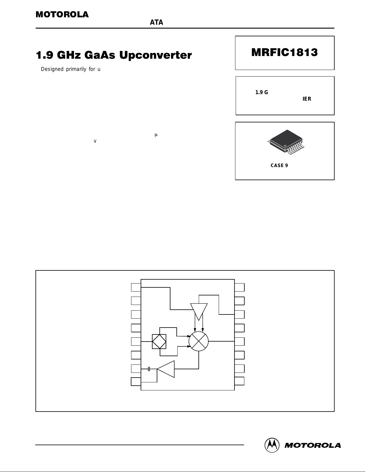
Designed primarily for use in wireless Personal Communication Systems
(PCS) applications such as Digital European Cordless Telephone (DECT),
Japan’s Personal Handy System (PHS) and the emerging North American
systems. The MRFIC1813 is also applicable to 2.4 GHz ISM equipment. The
device combines a balanced upmixer and a transmit exciter amplifier in a
low-cost TSSOP–16 package. Minimal off-chip matching is required while
allowing for maximum flexibility and efficiency. The mixer is optimized for
low–side injection and provides more than 12 dB of conversion gain with over 0
dBm output at 1 dB gain compression. Image filtering is implemented off-chip to
allow maximum flexibility. A CMOS compatible ENABLE pin allows standby
operation where the current drain is less than 250 mA.
Together with other devices from the MRFIC180X or the MRFIC240X series,
this GaAs IC family offers the complete transmit and receive functions, less LO
and filters, needed for a typical 1.8 GHz cordless telephone or 2.4 GHz ISM
band equipment.
• Usable Frequency Range = 1.7 to 2.5 GHz
• 15 dB Typ IF to RF Conversion Gain
• 3 dBm Power Output Typ, 0 dBm Minimum at 1 dB Gain Compression
• Simple Off-chip Matching for Maximum Flexibility
• Low Power Consumption = 75 mW (Typ)
• Single Bias Supply = 2.7 to 4.5 Volts
• Low LO Power Requirement = – 5 dBm (Typ)
• Low Cost Surface Mount Plastic Package
• Order MRFIC1813R2 for Tape and Reel.
R2 Suffix = 2,500 Units per 16 mm, 13 inch Reel.
• Device Marking = M1813
Order this document
by MRFIC1813/D
1.9 GHz UPMIXER AND
EXCITER AMPLIFIER
CASE 948C–03
(TSSOP–16)
REV 2
Motorola, Inc. 1997
MOTOROLA RF DEVICE DATA
V
DD1
N/C N/C
N/C
GND
LO IN
GND
RF OUT
V
DD2
1
2
3
4
5
6
7
8
EXCITER
MIXER
16
15
14
13
12
11
10
9
Pin Connections and Functional Block Diagram
TX ENABLE
IF IN
GND
V
DD3
GND
N/C
N/C
MRFIC1813
1
Page 2
MAXIMUM RATINGS
(TA = 25°C unless otherwise noted)
Ratings Symbol Limit Unit
Supply Voltage V
IF Input Power P
LO Input Power P
Enable Voltage TX ENABLE 5.5 Vdc
Storage Temperature Range T
Operating Ambient Temperature T
DD1
, V
DD2
IF
LO
stg
A
, V
DD3
5.5 Vdc
3 dBm
3 dBm
– 65 to +150 °C
– 30 to +85 °C
RECOMMENDED OPERATING RANGES
Parameter Symbol Value Unit
RF Output Frequency f
LO Input Frequency f
IF Input Frequency f
Supply Voltage V
TX Enable Voltage, ON TX ENABLE 2.7 to V
TX Enable Voltage, OFF TX ENABLE 0 to 0.2 Vdc
RF
LO
IF
DD
1.7 to 2.5 GHz
1.5 to 2.4 GHz
70 to 350 MHz
2.7 to 4.5 Vdc
DD
Vdc
ELECTRICAL CHARACTERISTICS (V
@ –15 dBm)
DD1,2,3,
Characteristic
IF to RF Small Signal Conversion Gain (PRF = –35 dBm) 12 15 — dB
RF Output 1 dB Gain Compression 0 3 — dBm
RF Output 3rd Order Intercept — 11 — dBm
LO Feedthrough to RF Port — –15 –10 dBm
Noise Figure — 11 — dB
Lower Sideband Output Power at RF Port — –10 –6 dBm
Supply Current TX Mode — 25 35 mA
Supply Current Standby Mode (TX ENABLE = 0 V , LO Of f) — 100 250
TX Enable Current — 3 —
V
DD1
C2
LO IN
RF OUT
V
DD2
C3
C1, C2, C3, C4 15 pF
C6 1 µF
R1 300 Ω
T1, T2 MICROSTRIP, Z0 = 73 Ω, θ = 29° @ 1.9 GHz
BOARD MATERIAL – GLASS/EPOXY, εr = 4.45,
DIELECTRIC THICKNESS = 0.018 INCH
C1
T1
TX ENABLE= 3 V, TA = 25°C, fLO = 1.65 GHz @ – 5 dBm, fIF = 250 MHz
Min Typ Max Unit
R1
L1
T2
TX ENABLE
C5
V
C4 C6
IF IN
DD3
1
2
3
4
5
6
7
8
EXCITER
MIXER
16
15
14
13
12
11
10
9
IF Frequency L1 C5
110 MHz 180 nH 12 pF
250 MHz 68 nH 5.6 pF
350 MHz 39 nH 3.9 pF
m
A
m
A
MRFIC1813
2
Figure 1. Applications Circuit Configuration
MOTOROLA RF DEVICE DATA
Page 3
18
17
16
15
14
13
12
11
, CONVERSION GAIN (dB)
C
10
G
9.0
8.0
–10
4 & 4.5 Vdc
PLO, LO INPUT POWER (dBm)
Figure 2. Conversion Gain versus LO Power Figure 3. Conversion Gain versus LO Power
18
VDD = 3 Vdc
fRF = 1.9 GHz
fIF = 250 MHz
PIF = –35 dBm
TA = 25
°
C
–4.0–8.0 –6.0 –2.0 0 –6.0 –4.0 –2.0 0
16
14
12
10
, CONVERSION GAIN (dB)
C
G
8.0
6.0
–10 –8.0
TA = –35°C
PLO, LO INPUT POWER (dBm)
25°C
85°C
fRF = 1.9 GHz
fIF = 250 MHz
PIF = –35 dBm
20
18
16
14
12
10
, CONVERSION GAIN (dB)
C
G
8.0
6.0
IF = 110 MHz
–8.0 –6.0 –4.0 2500
Figure 4. Conversion Gain versus LO Power Figure 5. Conversion Gain versus RF
16
15
14
13
12
11
10
9.0
, CONVERSION GAIN (dB)
C
G
8.0
7.0
6.0
TA = –35°C
fIF = 250 MHz
PIF = –35 dBm
PLO = –5 dBm
VDD = 3 Vdc
1800 1900
fRF, RF FREQUENCY (MHz)
250 MHz
fRF = 1.9 GHz
PIF = –35 dBm
VDD = 3 Vdc
TA = 25
PLO, LO POWER (dBm)
25°C
2000 22001700
2100
350 MHz
°
C
–2.0–10
85°C
2300 25002400
16
15
14
13
12
11
10
, CONVERSION GAIN (dB)
C
9.0
G
8.0
0
7.0
VDD = 3 Vdc
PRF = –35 dBm
fIF = 250 MHz
PLO = –5 dBm
TA = 25
°
C
fRF, RF FREQUENCY (MHz)
4 Vdc
4.5 Vdc
24002300220021002000190018001700
Frequency
18
16
14
12
10
, CONVERSION GAIN (dB)
C
G
8.0
6.0
IF = 110 MHz
PIF = –35 dBm
PLO = –5 dBm
TA = 25
°
C
1900 2000 210018001700
250 MHz
350 MHz
2300
fRF, RF FREQUENCY (GHz)
2400 25002200
Figure 6. Conversion Gain versus RF
Frequency
MOTOROLA RF DEVICE DATA
Figure 7. Conversion Gain versus RF
Frequency
MRFIC1813
3
Page 4

5.0
–5.0
–10
, RF OUTPUT POWER (dBm)
RF
–15
P
–20
10
0
–35
4 & 4.5 Vdc
VDD = 3 Vdc
fRF = 1.9 GHz
fIF = 250 MHz
PLO = –5 dBm
TA = 25
°
C
–20–30 –25 –15 –10 –25 –20 –15 0
PIF, IF INPUT POWER (dBm)
–5.0 0
5.0
–5.0
–10
–15
, RF OUTPUT POWER (dBm)
RF
P
–20
–25
10
0
TA = –35°C
–35 –30
25 & 85°C
PIF, IF INPUT POWER (dBm)
fRF = 1.9 GHz
PLO = –5 dBm
Figure 8. RF Output versus Input Power Figure 9. RF Output Power versus IF Input
Power
fIF = 250 MHz
VDD = 3 Vdc
–10 –5.0
10
5.0
0
–5.0
–10
, OUTPUT POWER (dBm)
–15
RF
P
–20
–25
IF = 110 MHz
–35 –30
Figure 10. RF Output versus IF Input Power Figure 11. Output Power versus IF Input
29
28
27
26
25
24
23
, SUPPLY CURRENT (mA)
DD
I
22
21
20
fRF = 1.9 GHz
fIF = 250 MHz
PLO = –5 dBm
TA = 25
–30 –25
5.0
0
–5.0
–10
250 & 350 MHz
–25 –20 –15 0
PIF, IF INPUT POWER (dBm) PIF, IF INPUT POWER (dBm)
fRF = 1.9 GHz
PLO = –5 dBm
VDD = 3 Vdc
TA = 25
°
C
–10 –5.0
–15
, RF OUTPUT POWER (dBm)
OUT
–20
P
–25
fIF = 110 MHz
Power
26.0
25.5
25.0
24.5
24.0
23.5
, SUPPLY CURRENT (mA)
DD
I
23.0
22.5
fRF = 1.9 GHz
fIF = 250 MHz
PLO = –5 dBm
VDD = 3 Vdc
TA = 25°C
–25 –20 –15–30–35
PIF, IF INPUT POWER (dBm)
4 Vdc
VDD = 3 Vdc
°
C
–15
–20 –10–35
PIF, IF INPUT POWER (dBm)
4.5 Vdc
–5.0 0
350 MHz
fRF = 2.45 GHz
PLO = –5 dBm
VDD = 3 Vdc
TA = 25
–35°C
85°C
250 MHz
°
C
–5.0
0–5.0–10–15–20–25–30
0–10
MRFIC1813
4
Figure 12. Supply Current versus IF Input
Power
Figure 13. Supply Current versus IF Input
Power
MOTOROLA RF DEVICE DATA
Page 5

24.5
0
24.0
23.5
23.0
22.5
22.0
21.5
21.0
–35
fRF = 1.9 GHz
PLO = –5 dBm
VDD = 3 Vdc
TA = 25
°
C
, SUPPLY CURRENT (mA)
DD
I
Figure 14. Supply Current versus IF Input
0
–2.0
–4.0
–6.0
–8.0
–10
–12
, LSB POWER (dBm)
–14
LSB
P
–16
–18
–20
4 & 4.5 Vdc
VDD = 3 Vdc
1800 1900 2000
250 MHz
350 MHz
–20–30 –25 –15 –10 1500 1600
PIF, IF INPUT POWER (dBm)
Power
21001700
2200
fRF, RF FREQUENCY (MHz)
IF = 110 MHz
–5.0 0
fIF = 250 MHz
PIF = –15 dBm
PLO = –5 dBm
TA = 25
°
C
24002300 2500
–5.0
IF = 110 MHz
–10
–15
–20
LO–RF FEEDTHROUGH (dBm)
–25
–30
1300 1400
350 MHz
FLO, LO FREQUENCY (MHz)
Figure 15. LO to RF Feedthrough versus LO
Frequency
25
20
15
10
, SUPPLY CURRENT (mA)
DD
5.0
I
0
TX EN (VOLTS)
250 MHz
PLO = –5 dBm
VDD = 3 Vdc
TA = 25
°
C
1900 20001700 1800 2100
VDD = 3 Vdc
TA = 25
°
C
3.02.52.01.51.00.50
Figure 16. Lower Side Band Power versus RF
Frequency
Figure 17. Supply Current versus Transmit
Enable V oltage
MOTOROLA RF DEVICE DATA
MRFIC1813
5
Page 6

f
IF Input LO Input RF Output
(MHz) R jX R jX R jX
70 8.3 –452.4
100 7.3 –318.5
150 7.1 –211.3
200 6.6 –156.4
250 6.5 –123.1
300 6.1 –100.7
350 5.7 –84.2
1100 62.5 3.1
1200 58.1 4.3
1300 53.7 4.7
1400 50.2 4.2
1500 47.3 3.9
1600 44.4 3.2
1700 42.0 1.6 30.4 33.6
1800 40.6 0.5 42.6 16.9
1900 39.6 –0.7 49.1 2.3
2000 38.7 –2.2 40.6 14.2
2100 38.2 –3.6 33.8 17.7
2200 38.4 –5.1 33.3 15.7
2300 38.9 –6.5 32.9 13.7
2400 39.5 –7.8 29.6 13.2
2500 27.4 11.9
(1) Includes T1 shown in Figure 1.
(1)
T able 1. Port Impedances versus Frequency
(VD1, VD2, VD3, TX EN = 3 Vdc)
APPLICATIONS INFORMATION
DESIGN CONSIDERATIONS
The MRFIC1813 combines a single–balanced MESFET
mixer with an exciter amplifier. It is usable for transmit frequencies from 1.7 to 2.5 GHz and IF frequencies from 70 to
350 MHz. The design is optimized for low–side local oscillator injection in hetrodyne transmit applications.
Minimal off–chip matching is required while allowing for
flexibility and performance optimization. An active balun is
employed at the IF port which gives good balance down to at
least 70 MHz. A passive splitter is used at the LO input to
complete the single–balanced configuration.
CIRCUIT CONSIDERATIONS
Figure 1 shows the application circuit used to gather the
data presented in the characterization curves. As shown in
Table 1, the IF port impedance is very high. Three hundred
ohms was chosen for R1 to shunt the IF port as a compromise of gain and bandwidth. A 50 Ω resistor can be used and
L1 and C5 eliminated to provide a broadband match. The
conversion gain is reduced to about 8 dB. Microstrip inductors T1 and T2 combine with inductance internal to the device to form RF chokes. Some tuning of the RF output can be
achieved with T1.
As with all RF devices, circuit layout is important. Controlled impedance lines should be used for all RF and IF interconnects. As shown in Figure 1, power supply by–passing
should be used to avoid device instability. Ground vias
should be included near all ground connections indicated in
the schematic. Off–chip components should be mounted as
close to the IC leads as possible.
EVALUATION BOARDS
Evaluation boards are available for RF Monolithic Integrated Circuits by adding a “TF” to the device type. For a
complete list of currently available boards and one in development for newly introduced products, please contact your
local Motorola Distributor or Sales Office.
MRFIC1813
6
MOTOROLA RF DEVICE DATA
Page 7

P ACKAGE DIMENSIONS
0.100 (0.004)
-T-
SEATING
PLANE
PIN 1
IDENTIFICATION
M
J1
J
L
18
C
D
K
SECTION A–A
A
-P-
16x REFK
0.200 (0.008)MT
916
B
G
H
A
K1
M
NOTES:
1. DIMENSIONING AND TOLERANCING PER ANSI
Y14.5M, 1982.
2. CONTROLLING DIMENSION: MILLIMETER.
3. DIMENSION A DOES NOT INCLUDE MOLD
FLASH, PROTRUSIONS OR GATE BURRS. MOLD
FLASH OR GATE BURRS SHALL NOT EXCEED
0.15 (0.006) PER SIDE.
4. DIMENSION B DOES NOT INCLUDE
INTERLEAD FLASH OR PROTRUSION.
INTERLEAD FLASH OR PROTRUSION SHALL NOT
EXCEED 0.25 (0.010) PER SIDE.
5. DIMENSION K DOES NOT INCLUDE DAMBAR
PROTRUSION. ALLOWABLE DAMBAR
PROTRUSION SHALL BE 0.08 (0.003) TOTAL
EXCESS OF THE K DIMENSION AT MAXIMUM
MATERIAL CONDITION.
6. TERMINAL NUMBERS ARE SHOWN FOR
REFERENCE ONLY.
7. DIMENSIONS A AND B ARE TO BE
DETERMINED AT DATUM PLANE –U–.
MILLIMETERS
DIMAMIN MAX MIN MAX
-U-
––– 5.10 ––– 0.200
B 4.30 4.50 0.169 0.177
C ––– 1.20 ––– 0047
D 0.05 0.25 0.002 0.010
F 0.45 0.55 0.018 0.022
G 0.65 BSC 0.026 BSC
H 0.22 0.23 0.009 0.010
J 0.09 0.24 0.004 0.009
J1 0.09 0.18 0.004 0.007
K 0.16 0.32 0.006 0.013
K1 0.16 0.26 0.006 0.010
L 6.30 6.50 0.248 0.256
M 0 10 0 10
°°°°
INCHES
A
F
CASE 948C–03
ISSUE B
MOTOROLA RF DEVICE DATA
MRFIC1813
7
Page 8

Motorola reserves the right to make changes without further notice to any products herein. Motorola makes no warranty , representation or guarantee regarding
the suitability of its products for any particular purpose, nor does Motorola assume any liability arising out of the application or use of any product or circuit, and
specifically disclaims any and all liability, including without limitation consequential or incidental damages. “T ypical” parameters which may be provided in Motorola
data sheets and/or specifications can and do vary in different applications and actual performance may vary over time. All operating parameters, including “Typicals”
must be validated for each customer application by customer’s technical experts. Motorola does not convey any license under its patent rights nor the rights of
others. Motorola products are not designed, intended, or authorized for use as components in systems intended for surgical implant into the body, or other
applications intended to support or sustain life, or for any other application in which the failure of the Motorola product could create a situation where personal injury
or death may occur. Should Buyer purchase or use Motorola products for any such unintended or unauthorized application, Buyer shall indemnify and hold Motorola
and its officers, employees, subsidiaries, affiliates, and distributors harmless against all claims, costs, damages, and expenses, and reasonable attorney fees
arising out of, directly or indirectly, any claim of personal injury or death associated with such unintended or unauthorized use, even if such claim alleges that
Motorola was negligent regarding the design or manufacture of the part. Motorola and are registered trademarks of Motorola, Inc. Motorola, Inc. is an Equal
Opportunity/Affirmative Action Employer.
How to reach us:
USA/EUROPE /Locations Not Listed: Motorola Literature Distribution; JAPAN: Nippon Motorola Ltd.: SPD, Strategic Planning Office, 4–32–1,
P.O. Box 5405, Denver, Colorado 80217. 303–675–2140 or 1–800–441–2447 Nishi–Gotanda, Shinagawa–ku, Tokyo 141, Japan. 81–3–5487–8488
Mfax: RMFAX0@email.sps.mot.com – TOUCHTONE 602–244–6609 ASIA/PACIFIC: Motorola Semiconductors H.K. Ltd.; 8B Tai Ping Industrial Park,
– US & Canada ONLY 1–800–774–1848 51 Ting Kok Road, T ai Po, N.T., Hong Kong. 852–26629298
INTERNET: http://motorola.com/sps
Mfax is a trademark of Motorola, Inc.
MRFIC1813
8
◊
MOTOROLA RF DEVICE DATA
MRFIC1813/D
 Loading...