

Page 1
SEMICONDUCTOR TECHNICAL DATA
The MRFIC Line
Order this document
by MRFIC1808/D
Designed primarily for use in wireless Personal Communication Systems
(PCS) applications such as Digital European Cordless Telephone (DECT),
Japan’s Personal Handy System (PHS) and the emerging North American
systems as a preamp for discrete or integrated downmixers. The MRFIC1808
is a two–stage low noise amplifier in a low–cost SO–8 package. The amplifier
can be matched to optimize gain or noise figure with simple off–chip input
matching. The design employs a novel stacked MESFET design which reuses
bias current for the highest gain at minimal current. A CMOS compatible
RECEIVE ENABLE pin allows for very low standby current while the system is
in transmit mode.
• Usable Frequency Range = 1.7 to 2.1 GHz
• 19 dB Typ Gain
• 1.6 dB Typ Noise Figure
• Simple Off–chip Matching for Maximum Gain/Noise Figure Flexi-
bility
• High Reverse Isolation = –34 dB (Typ)
• Low Power Consumption = 13 mW (Typ)
• Single Bias Supply = 2.7 to 4.5 Volts
• Low Standby Current = 8 µA (Typ)
• Low Cost Surface Mount Plastic Package
• Order MRFIC1808R2 forTape and Reel.
R2 Suffix = 2,500 Units per 16 mm, 13 inch Reel.
• Device Marking = M1808
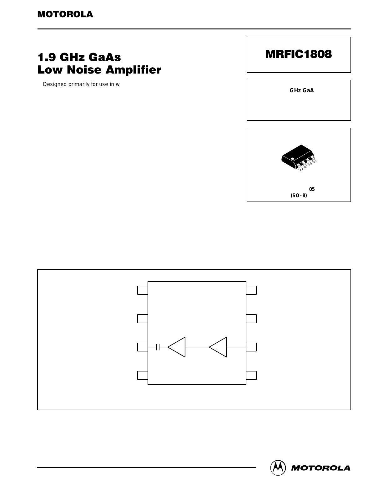
1.9 GHz GaAs
LOW NOISE
AMPLIFIER
CASE 751–05
(SO–8)
REV 1
1
V
DD1
2
N/C
RF OUT
LNA CAP
3
4
Pin Connections and Functional Block Diagram
RX ENABLE
8
7
GND
RF IN
6
5
GND
Motorola, Inc. 1997
MRFIC1808MOTOROLA RF DEVICE DATA
1
Page 2
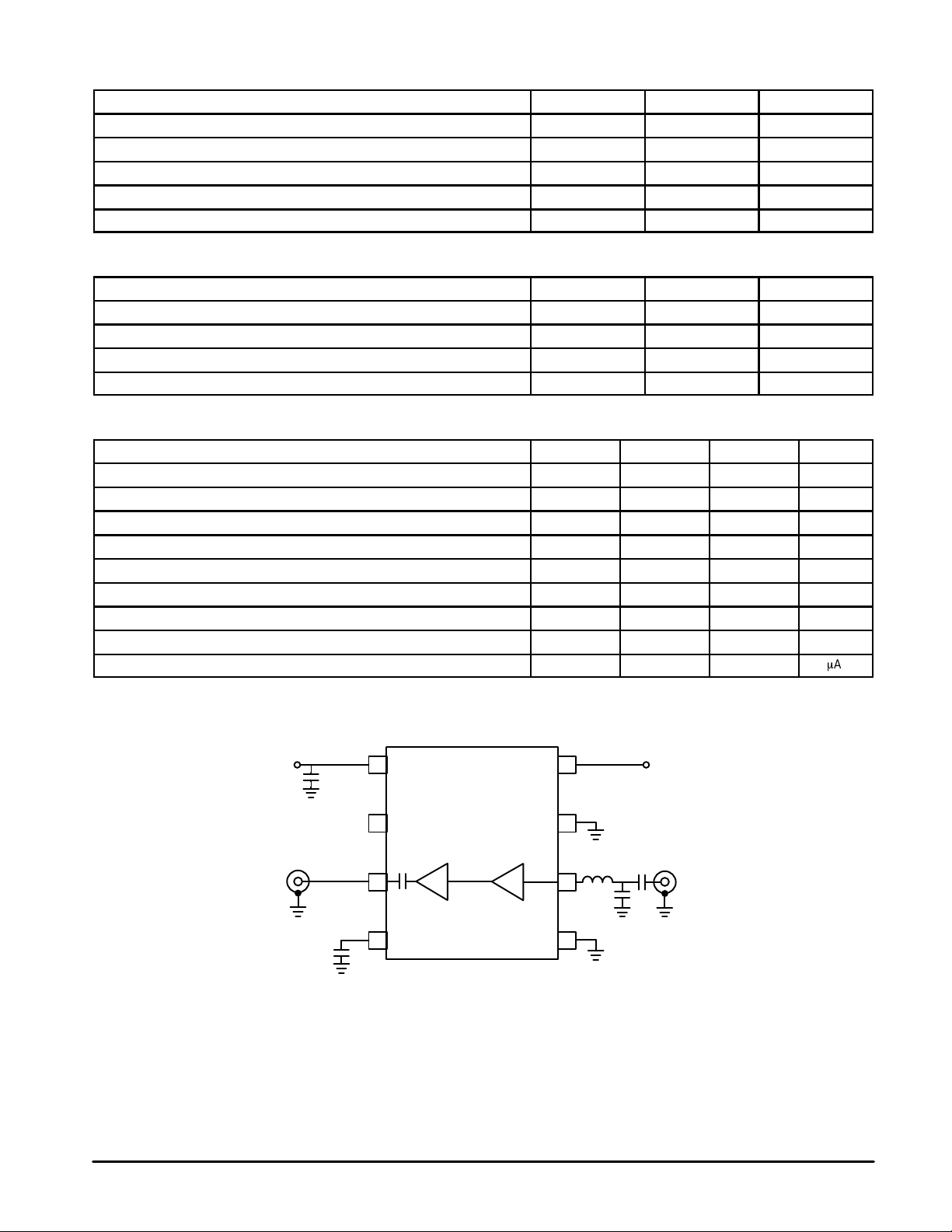
MAXIMUM RATINGS (T
Supply Voltage V
RF Input Power P
Enable Voltage RX ENABLE 5.5 Vdc
Storage Temperature Range T
Operating Ambient Temperature T
= 25°C unless otherwise noted)
A
Rating
Symbol Limit Unit
DD
RF
stg
A
5.5 Vdc
3 dBm
– 65 to +150 °C
– 30 to +85 °C
RECOMMENDED OPERATING RANGES
Parameter Symbol Value Unit
RF Frequency f
Supply Voltage V
RX Enable Voltage, ON RX ENABLE 2.7 to V
RX Enable Voltage, OFF RX ENABLE 0 to 0.2 Vdc
RF
DD
1.7 to 2.1 GHz
2.7 to 4.5 Vdc
DD
Vdc
ELECTRICAL CHARACTERISTICS (V
Characteristic
RF Gain 16.0 19 — dB
SSB Noise Figure — 1.6 — dB
RF Output 3rd Order Intercept Point — 13 — dBm
Output 1 dB Gain Compression –3.0 1 — dBm
Reverse Isolation (s12) — –34 — dB
Input Return Loss — –12 — dB
Output Return Loss — –15 — dB
Supply Current RX Mode — 4.2 6.5 mA
Supply Current Standby Mode (RX ENABLE = 0 V) — 8 25
V
DD
RF OUT
= 3 V, TA = 25°C, RF = 1.9 GHz, RX ENABLE = 3 V, Tested in Circuit Shown in Figure 1)
DD
Min Typ Max Unit
C4
1
2
3
8
7
L1
6
C2
RX ENABLE
C3
RF IN
m
A
MRFIC1808
2
C1
4
C1 2 pF
C2 1.8 pF
C3, C4 22 pF
L1 5.6 nH
5
Figure 1. Applications Circuit Configuration
MOTOROLA RF DEVICE DATA
Page 3
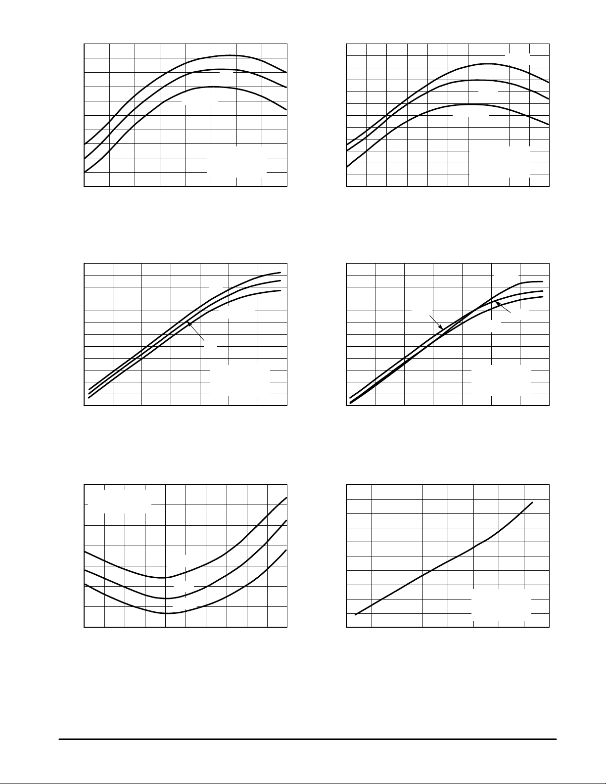
21
20
19
18
G, GAIN (dB)
17
16
1.8
5 V
4 V
VDD = 3 V
Pin = –30 dBm
TA = 25
°
C
RX ENABLE = 3 V
1.85 1.9 1.95 2
f, FREQUENCY (GHz)
21
20
19
18
G, GAIN (dB)
17
16
15
1.82 1.86 1.88 1.94 1.96 1.98
1.8
–30°C
25°C
TA = 85°C
Pin = –30 dBm
VDD = 3 V
RX ENABLE = 3 V
1.84 1.9 1.92 2
f, FREQUENCY (GHz)
Figure 2. Gain versus Frequency
6
3
0
–3
–6
out
P , OUTPUT POWER (dBm)
–9
–12
–28 –22 –19
–31
–25 –16 –13 –10
Pin, INPUT POWER (dBm)
4 V
Figure 4. Output Power versus Input Power
4.5
VDD = 3 – 5 V
4
RX ENABLE = V
3.5
3
2.5
2
NF, NOISE FIGURE (dB)
1.5
1
1.7
DD
TA = 85°C
25°C
–30°C
1.8 2 2.1
1.9 2.2
f, FREQUENCY (GHz)
5 V
VDD = 3 V
TA = 25°C
f = 1.9 GHz
RX ENABLE = 3 V
–3
–6
out
P , OUTPUT POWER (dBm)
–9
–12
5.25
4.75
4.5
, SUPPLY CURRENT (mA)
DD
I
4.25
Figure 3. Gain versus Frequency
6
3
0
–31
–28 –22 –19
–25 –16 –13 –10
25°C
Pin, INPUT POWER (dBm)
–30°C
TA = 85°C
VDD = 3 V
f = 1.9 GHz
RX ENABLE = 3 V
Figure 5. Output Power versus Input Power
5
f = 1.9 GHz
TA = 25
°
RX ENABLE = 3 V
4
2.8
3.1 3.7 4
3.4 5.2
VDD, SUPPLY VOLT AGE (VOLTS)
4.3
4.6
25°C
C
4.9
Figure 6. Noise Figure versus Frequency
Figure 7. Supply Current versus V oltage
MRFIC1808MOTOROLA RF DEVICE DATA
3
Page 4

–33
–34
–35
–36
REVERSE ISOLATION (dB)
–37
1.8
VDD = 3 V
4 V
5 V
Pin = –30 dBm
TA = 25
°
C
RX ENABLE = 3 V
1.84 1.9 1.92 21.82 1.86 1.88 1.94 1.96 1.98
f, FREQUENCY (GHz)
–32
–33
–34
–35
REVERSE ISOLATION (dB)
–36
–37
1.8
–30°C
25°C
TA = 85°C
Pin = –30 dBm
VDD = 3 V
RX ENABLE = 3 V
1.84 1.9 1.92 21.82 1.86 1.88 1.94 1.96 1.98
f, FREQUENCY (GHz)
Figure 8. Reverse Isolation versus Frequency
Figure 9. Reverse Isolation versus Frequency
MRFIC1808
4
MOTOROLA RF DEVICE DATA
Page 5

T able 1. Scattering Parameters (VDD = 3 V olts, TA = 25°C, RX ENABLE = 3 Volts, 50 W System)
f
S
f
(MHz)
1500 0.859 –40.95 2.58 139.07 0.013 103.72 0.583 –79.05
1530 0.870 –41.50 2.79 134.79 0.013 105.63 0.530 –80.94
1560 0.866 –42.06 3.01 130.60 0.013 99.14 0.474 –82.85
1590 0.871 –42.92 3.18 125.11 0.014 98.40 0.412 –83.57
1620 0.873 –43.47 3.30 118.70 0.012 98.00 0.348 –83.11
1650 0.876 –43.60 3.37 112.85 0.012 97.39 0.285 –80.54
1680 0.877 –44.86 3.52 106.23 0.012 92.68 0.229 –73.01
1710 0.880 –45.35 3.68 100.77 0.011 93.90 0.186 –60.35
1740 0.876 –46.03 3.80 94.40 0.012 93.12 0.168 –40.74
1770 0.876 –47.22 3.87 88.75 0.011 88.55 0.182 –20.50
1800 0.885 –48.69 3.98 82.96 0.010 88.40 0.221 –6.82
1830 0.879 –48.55 3.98 76.83 0.010 89.46 0.272 –0.29
1860 0.881 –49.87 3.98 71.11 0.009 94.75 0.324 3.05
1890 0.885 –50.71 4.00 66.38 0.009 97.00 0.376 4.39
1920 0.878 –51.81 4.09 61.64 0.009 88.22 0.425 4.25
1950 0.873 –52.42 4.19 56.66 0.008 87.57 0.474 3.79
1980 0.860 –52.98 4.15 51.32 0.007 88.75 0.522 2.22
2010 0.866 –54.24 3.98 44.93 0.006 100.17 0.564 0.85
2040 0.859 –56.12 3.85 40.93 0.005 87.86 0.599 –0.87
2070 0.861 –56.69 3.89 37.99 0.004 99.30 0.634 –3.01
2100 0.850 –57.79 4.04 35.71 0.004 98.94 0.661 –4.59
2130 0.844 –58.53 4.18 31.89 0.004 118.15 0.691 –6.96
2160 0.834 –60.21 4.21 26.88 0.003 137.84 0.714 –8.94
2190 0.834 –61.26 4.15 22.38 0.003 141.53 0.734 –11.49
2220 0.830 –62.53 4.17 18.75 0.004 –164.13 0.760 –13.48
2250 0.817 –63.84 4.22 14.85 0.004 –172.30 0.776 –15.27
2280 0.812 –64.69 4.21 9.17 0.005 –165.76 0.787 –17.20
2310 0.811 –66.64 4.14 4.09 0.006 –148.57 0.805 –19.42
2340 0.800 –67.89 3.95 1.20 0.007 –153.96 0.808 –21.63
2370 0.794 –69.40 3.83 0.29 0.008 –144.49 0.819 –23.38
2400 0.791 –72.05 3.88 0.33 0.009 –133.12 0.822 –26.10
2430 0.784 –73.59 4.09 –2.06 0.012 –138.06 0.826 –28.21
2460 0.774 –75.60 4.30 –8.63 0.014 –138.55 0.824 –30.43
2490 0.769 –78.81 4.33 –16.94 0.015 –146.05 0.821 –32.72
2520 0.751 –80.46 4.31 –23.37 0.018 –148.25 0.815 –35.42
2550 0.737 –83.20 4.23 –27.46 0.021 –149.08 0.798 –37.56
2580 0.707 –86.12 4.08 –32.67 0.024 –155.44 0.767 –39.31
|S11| ∠ φ |S21| ∠ φ |S12| ∠ φ |S22| ∠ φ
11
S
21
S
12
S
22
MRFIC1808MOTOROLA RF DEVICE DATA
5
Page 6

T able 2. Scattering Parameters (VDD = 4 V olts, TA = 25°C, RX ENABLE = 3 Volts, 50 W System)
f
S
f
(MHz)
1500 0.849 –40.63 2.83 138.31 0.013 101.12 0.592 –78.76
1530 0.854 –41.00 3.07 134.02 0.012 99.54 0.537 –80.92
1560 0.852 –41.65 3.30 129.90 0.012 97.89 0.482 –82.91
1590 0.855 –42.76 3.50 124.44 0.013 103.09 0.421 –84.04
1620 0.861 –43.15 3.63 118.09 0.013 104.42 0.357 –84.20
1650 0.862 –43.22 3.73 112.01 0.012 95.75 0.293 –82.14
1680 0.861 –44.49 3.89 106.04 0.012 95.43 0.233 –75.91
1710 0.861 –44.93 4.07 100.17 0.011 99.73 0.187 –63.54
1740 0.869 –45.60 4.19 94.14 0.011 94.00 0.164 –43.94
1770 0.864 –46.48 4.30 87.75 0.011 95.67 0.173 –22.19
1800 0.870 –48.17 4.41 82.13 0.011 88.56 0.210 –7.42
1830 0.860 –48.09 4.41 75.97 0.010 88.92 0.258 0.31
1860 0.866 –49.28 4.41 70.37 0.010 96.31 0.313 3.91
1890 0.870 –50.19 4.46 65.24 0.009 93.39 0.367 5.28
1920 0.861 –50.75 4.54 60.65 0.008 90.74 0.417 5.60
1950 0.852 –51.77 4.66 55.96 0.008 89.58 0.468 4.75
1980 0.849 –52.40 4.56 50.46 0.007 84.42 0.518 3.22
2010 0.847 –53.50 4.40 44.25 0.006 94.48 0.561 1.68
2040 0.847 –55.19 4.25 39.96 0.005 88.62 0.597 –0.03
2070 0.847 –55.75 4.29 37.08 0.004 109.85 0.633 –2.25
2100 0.842 –56.92 4.47 34.67 0.005 103.26 0.664 –3.78
2130 0.830 –57.36 4.61 30.80 0.004 125.77 0.694 –6.23
2160 0.823 –59.26 4.66 26.03 0.004 122.00 0.717 –8.30
2190 0.820 –60.09 4.57 21.27 0.004 152.31 0.742 –10.87
2220 0.820 –61.37 4.57 17.70 0.002 160.02 0.762 –13.04
2250 0.812 –63.01 4.63 13.81 0.003 176.88 0.778 –14.80
2280 0.801 –63.88 4.61 8.47 0.004 –165.16 0.792 –17.00
2310 0.802 –65.68 4.54 2.90 0.005 –156.21 0.807 –19.20
2340 0.789 –67.07 4.32 0.38 0.007 –141.83 0.815 –21.21
2370 0.781 –68.28 4.21 –1.24 0.008 –144.89 0.821 –23.34
2400 0.775 –70.61 4.23 –0.61 0.010 –143.18 0.826 –25.75
2430 0.771 –72.01 4.47 –2.85 0.012 –140.04 0.829 –28.07
2460 0.764 –74.59 4.70 –9.44 0.012 –144.28 0.829 –30.56
2490 0.759 –77.25 4.72 –17.93 0.015 –149.63 0.826 –32.63
2520 0.743 –78.88 4.69 –24.28 0.017 –148.60 0.820 –35.12
2550 0.730 –81.98 4.58 –28.44 0.021 –148.70 0.802 –37.38
2580 0.700 –85.55 4.45 –33.64 0.022 –157.99 0.772 –39.29
|S11| ∠ φ |S21| ∠ φ |S12| ∠ φ |S22| ∠ φ
11
S
21
S
12
S
22
MRFIC1808
MOTOROLA RF DEVICE DATA
6
Page 7

T able 3. Scattering Parameters (VDD = 5 V olts, TA = 25°C, RX ENABLE = 3 Volts, 50 W System)
f
S
f
(MHz)
1500 0.830 –40.58 3.12 137.17 0.011 98.73 0.600 –78.51
1530 0.839 –41.24 3.39 132.69 0.011 101.93 0.548 –80.73
1560 0.836 –41.75 3.64 128.74 0.012 96.66 0.492 –82.85
1590 0.842 –42.35 3.85 123.33 0.013 99.33 0.433 –84.11
1620 0.848 –42.88 4.02 116.83 0.012 101.06 0.370 –84.63
1650 0.843 –43.41 4.11 110.95 0.012 95.15 0.306 –82.83
1680 0.844 –44.37 4.30 104.87 0.012 96.02 0.243 –77.32
1710 0.849 –45.07 4.49 99.42 0.012 96.86 0.193 –66.79
1740 0.852 –45.25 4.64 93.23 0.010 99.66 0.163 –48.45
1770 0.848 –46.18 4.75 87.02 0.012 88.90 0.164 –26.11
1800 0.856 –47.76 4.88 81.25 0.011 93.18 0.200 –9.04
1830 0.850 –47.99 4.87 75.09 0.010 90.25 0.247 –0.08
1860 0.850 –48.93 4.90 69.14 0.009 88.62 0.301 3.73
1890 0.849 –49.88 4.96 64.08 0.009 93.94 0.355 5.69
1920 0.846 –50.72 5.02 59.31 0.009 93.67 0.407 6.01
1950 0.837 –51.45 5.15 54.55 0.007 90.89 0.459 5.70
1980 0.830 –52.33 5.07 48.85 0.008 98.84 0.511 4.17
2010 0.831 –52.97 4.89 42.81 0.006 90.07 0.557 2.40
2040 0.831 –55.08 4.72 38.38 0.004 100.73 0.593 0.51
2070 0.829 –55.58 4.74 35.43 0.005 96.39 0.631 –1.55
2100 0.823 –56.53 4.95 32.95 0.004 122.68 0.661 –3.57
2130 0.815 –57.23 5.10 29.26 0.004 112.15 0.691 –5.96
2160 0.805 –58.81 5.14 24.21 0.004 132.80 0.718 –7.96
2190 0.802 –59.57 5.04 19.45 0.004 136.20 0.739 –10.56
2220 0.801 –60.70 5.05 15.80 0.003 178.25 0.762 –12.60
2250 0.791 –62.24 5.11 12.01 0.004 170.40 0.780 –14.52
2280 0.781 –62.95 5.08 6.42 0.005 –172.19 0.793 –16.63
2310 0.786 –64.98 4.97 1.09 0.006 –169.11 0.811 –18.96
2340 0.773 –66.05 4.74 –1.76 0.006 –150.31 0.818 –21.10
2370 0.766 –67.23 4.60 –2.91 0.008 –143.53 0.821 –23.29
2400 0.763 –69.83 4.64 –2.54 0.009 –146.46 0.827 –25.81
2430 0.757 –71.49 4.89 –4.89 0.011 –141.36 0.832 –27.88
2460 0.750 –73.61 5.12 –11.49 0.012 –147.16 0.832 –30.37
2490 0.742 –76.17 5.17 –19.88 0.014 –145.27 0.827 –32.68
2520 0.726 –78.01 5.10 –26.09 0.016 –145.14 0.820 –35.26
2550 0.712 –81.26 5.01 –30.13 0.018 –150.98 0.805 –37.48
2580 0.686 –84.54 4.81 –35.31 0.022 –155.55 0.771 –39.32
|S11| ∠ φ |S21| ∠ φ |S12| ∠ φ |S22| ∠ φ
11
S
21
S
12
S
22
MRFIC1808MOTOROLA RF DEVICE DATA
7
Page 8

P ACKAGE DIMENSIONS
C
A
A1
D
58
0.25MB
E
1
B
e
H
4
M
h
X 45
_
q
C
A
SEATING
PLANE
0.10
L
B
SS
A0.25MCB
NOTES:
1. DIMENSIONING AND TOLERANCING PER ASME
Y14.5M, 1994.
2. DIMENSIONS ARE IN MILLIMETERS.
3. DIMENSION D AND E DO NOT INCLUDE MOLD
PROTRUSION.
4. MAXIMUM MOLD PROTRUSION 0.15 PER SIDE.
5. DIMENSION B DOES NOT INCLUDE MOLD
PROTRUSION. ALLOWABLE DAMBAR
PROTRUSION SHALL BE 0.127 TOTAL IN EXCESS
OF THE B DIMENSION AT MAXIMUM MATERIAL
CONDITION.
MILLIMETERS
DIM MIN MAX
A 1.35 1.75
A1 0.10 0.25
B 0.35 0.49
C 0.18 0.25
D 4.80 5.00
E
3.80 4.00
1.27 BSCe
H 5.80 6.20
h
0.25 0.50
L 0.40 1.25
0 7
q
__
CASE 751–05
ISSUE S
Motorola reserves the right to make changes without further notice to any products herein. Motorola makes no warranty , representation or guarantee regarding
the suitability of its products for any particular purpose, nor does Motorola assume any liability arising out of the application or use of any product or circuit, and
specifically disclaims any and all liability, including without limitation consequential or incidental damages. “T ypical” parameters which may be provided in Motorola
data sheets and/or specifications can and do vary in different applications and actual performance may vary over time. All operating parameters, including “Typicals”
must be validated for each customer application by customer’s technical experts. Motorola does not convey any license under its patent rights nor the rights of
others. Motorola products are not designed, intended, or authorized for use as components in systems intended for surgical implant into the body, or other
applications intended to support or sustain life, or for any other application in which the failure of the Motorola product could create a situation where personal injury
or death may occur. Should Buyer purchase or use Motorola products for any such unintended or unauthorized application, Buyer shall indemnify and hold Motorola
and its officers, employees, subsidiaries, affiliates, and distributors harmless against all claims, costs, damages, and expenses, and reasonable attorney fees
arising out of, directly or indirectly, any claim of personal injury or death associated with such unintended or unauthorized use, even if such claim alleges that
Motorola was negligent regarding the design or manufacture of the part. Motorola and are registered trademarks of Motorola, Inc. Motorola, Inc. is an Equal
Opportunity/Affirmative Action Employer.
How to reach us:
USA/EUROPE/Locations Not Listed: Motorola Literature Distribution; JAPAN: Nippon Motorola Ltd.: SPD, Strategic Planning Office, 4–32–1,
P.O. Box 5405, Denver, Colorado 80217. 303–675–2140 or 1–800–441–2447 Nishi–Gotanda, Shinagawa–ku, Tokyo 141, Japan. 81–3–5487–8488
Mfax: RMFAX0@email.sps.mot.com – TOUCHTONE 602–244–6609 ASIA/PACIFIC: Motorola Semiconductors H.K. Ltd.; 8B Tai Ping Industrial Park,
INTERNET: http://motorola.com/sps
MRFIC1808
– US & Canada ONLY 1–800–774–1848 51 Ting Kok Road, T ai Po, N.T., Hong Kong. 852–26629298
◊
Mfax is a trademark of Motorola, Inc.
MOTOROLA RF DEVICE DATA
MRFIC1808/D
8
 Loading...