

Page 1
SEMICONDUCTOR TECHNICAL DATA
The MRFIC Line
This two–stage class AB monolithic GaAs amplifier in a low–cost 16 lead
plastic package is designed for output or driver applications in 1.9 GHz PCS
handsets and basestations. The design is optimized for 3.0 Volt operation in
systems such as Japan’s PHS, Europe’s DECT and the emerging North
American PCS services. With modifications to the simple off–chip matching, the
device can be used in other applications from 1.5 to 2.5 GHz.
• High Output Capability = 27 dBm Typical P
21.5 dBm Typical with PHS Format
• High Gain = 21 dB Typical Small Signal, 20 dB at P
• Low Current Drain = 170 mA Typical with PHS Format
250 mA Typical with DECT Format
• Low–Cost, Low Profile Plastic TSSOP Package
• Order MRFIC1805R2 for Tape and Reel.
R2 Suffix = 2,500 Units per 16 mm, 13 inch Reel.
• Device Marking = M1805
sat
= 22 dBm
out
Order this document
by MRFIC1805/D
1.9 GHz
POWER AMPLIFIER
GaAs MONOLITHIC
INTEGRATED CIRCUIT
CASE 948C–03
(TSSOP–16)
ABSOLUTE MAXIMUM RATINGS (TA = 25_C unless otherwise noted)
Ratings Symbol Value Unit
Supply Voltage VDD, VD1,
Supply Voltage V
RF Input Power RF
Drain Current I
Thermal Resistance, Junction to Air R
Operating Junction Temperature T
Ambient Operating Temperature T
Storage Temperature T
PCNTRL
16
GND
15
GND
V
D1
RF OUT/
GND N/C
V
D2
V
D2
SS
in
DD
θJA
J
A
stg
RF OUT/
V
D2
6 Vdc
–4 Vdc
+10 dBm
500 mA
240 /W
+175
–30 to +85
–65 to +125
91011121314
_
C
_
C
_
C
REV 1
Motorola, Inc. 1997
MOTOROLA RF DEVICE DATA
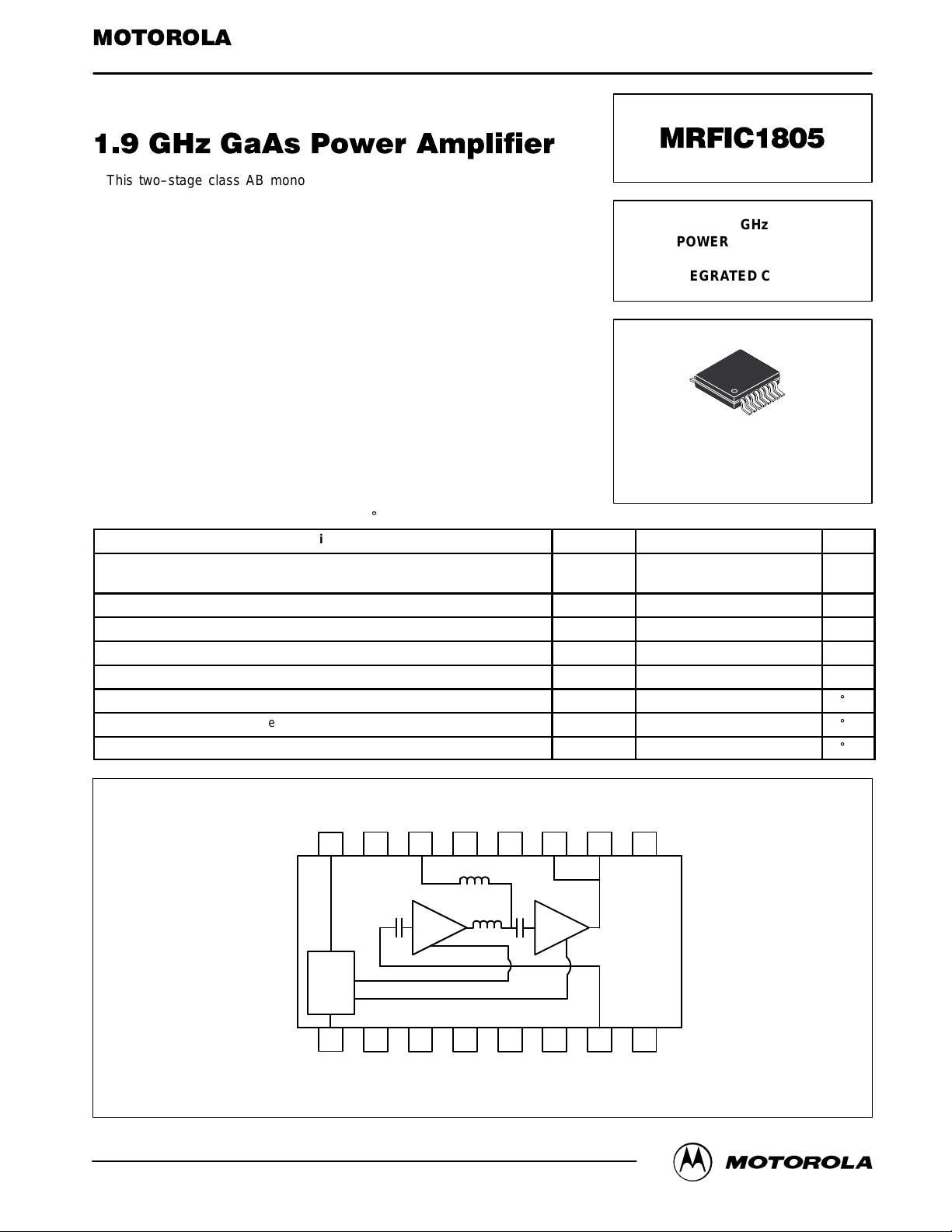
GATE
BIAS
1
234
V
GND GND
SS
GND
GND GND N/C
RF IN
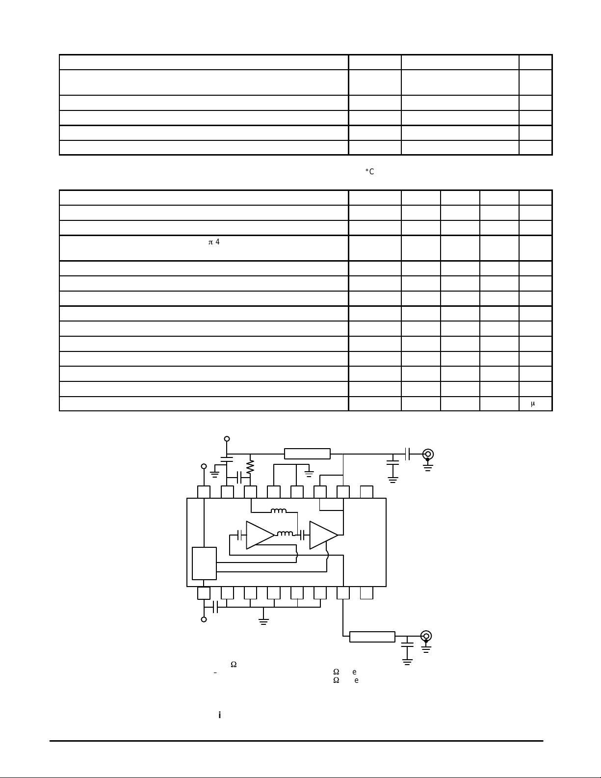
Pin Connections and Functional Block Diagram
8765
MRFIC1805
1
Page 2
RECOMMENDED OPERATING CONDITIONS
Parameter Symbol Value Unit
Supply Voltage VDD, VD1,
Supply Voltage V
PA Control Voltage PCNTRL 0.0 to V
RF Input Power P
Operating Frequency Range f
V
D2
SS
in
OP
2.7 to 5 Vdc
–2.5 Vdc
–20 to +10 dBm
1500 to 2200 MHz
DD
Vdc
ELECTRICAL CHARACTERISTICS (V
IDQ = 125 mA, circuit configuration as shown in Figure 1)
Characteristic
Power Output, Saturation P
RF Output Power P
Adjacent Channel Power Ratio (384 Kbps p/4 DQPSK Signal,
600 kHz Offset, P
RF Output 1 dB Compression P
2nd Harmonic Output – – –40 – dBc
3rd Harmonic Output – – –40 – dBc
Supply Current I
Supply Current I
Supply Current I
Input Return Loss – – 13 – dB
Reverse Isolation – – 31 – dB
Output Third Intercept – – 34 – dBm
Turn On Time – – 1 –
= 21 dBm
out
PCNTRL
= VD2 = 3 Vdc, Vss = –2.5 Vdc, TA= 25_C, f = 1.9 GHz, Pin = +2 dBm, PCNTRL set for
D1
Symbol Min Typ Max Unit
23 25 – dBm
20 21.5 – dBm
– –58 –55 dBc
22 24 – dBm
– 170 210 mA
– 200 300 µA
– 220 300 µA
C5
RF OUT
C3
SAT
out
P
ACP
1dB
DD
SS
PCNTRL
V
DD
C4
T2
R1
C2
m
s
MRFIC1805
2
15
16
GATE
BIAS
1
C6
V
SS
R1 – 22
C1 – 1.2 pF
C2 – 2.2 pF
C3, C6 – 330 pF
34
2
W
C4, C5, – 22 pF
T1 – 100 W Line, 7 mm
T2 – 100 W Line, 20 mm
Board Material – 30 MIL FR4
Connectors – SMA Type
Figure 1. Applications Circuit Configuration
91011121314
8765
T1
C1
RF IN
MOTOROLA RF DEVICE DATA
Page 3
TYPICAL CHARACTERISTICS
30
25
20
15
10
, OUTPUT POWER (dBm)
5
out
P
0
–5
–15 –5
–10
Pin, INPUT POWER (dBm)
2.5 V
Figure 2. Output Power versus Input Power
30
25
20
15
10
, OUTPUT POWER (dBm)
5
out
P
0
–5
–20
85°C
–35°C
–10 10
Pin, INPUT POWER (dBm)
TA = 25°C
–5–15 5
VDD = 3.5 V
f = 1.9 GHz
I
DDQ
TA = 25
0
f = 1.9 GHz
I
DDQ
VDD = 3.0 V
0
3.0 V
= 125 mA
°
C
= 125 mA
30
25
20
15
10
, OUTPUT POWER (dBm)
5
out
P
0
–5
105
–20 0–20
–15
150 mA
125 mA
–10 –5
Pin, INPUT POWER (dBm)
I
DDQ
= 190 mA
100 mA
f = 1.9 GHz
VDD = 3.0 V
TA = 25
°
C
105
Figure 3. Output Power versus Input Power
300
250
VDD = 3.5 V
200
150
, SUPPLY CURRENT (mA)
DD
I
100
50
–15 –10–20
3.0 V
2.5 V
–5 0 10
Pin, INPUT POWER (dBm)
f = 1.9 GHz
I
= 125 mA
DDQ
TA = 25
°
C
5
Figure 4. Output Power versus Input Power
300
250
I
= 190 mA
200
150
, SUPPLY CURRENT (mA)
DD
I
100
50
–20
DDQ
150 mA
125 mA
100 mA
–10 0
Pin, INPUT POWER (dBm)
–5
Figure 6. Supply Current versus Input Power
MOTOROLA RF DEVICE DATA
f = 1.9 GHz
VDD = 3.0 V
TA = 25
°
C
510
Figure 5. Supply Current versus Input Power
300
VDD = 3.5 V
250
200
150
100
, SUPPLY CURRENT (mA)
DD
I
50
0
0.5–15
3.0 V
1.0
1.5
P
, CONTROL VOLTAGE (V)
CNTRL
2.5 V
f = 1.9 GHz
I
= 125 mA
DDQ
Pin = +10 dBm
TA = 25
°
2.0 2.5 3.0
Figure 7. Supply Current versus Control Voltage
MRFIC1805
C
3.50.0
3
Page 4

TYPICAL CHARACTERISTICS
30
25
3.0 V
20
, OUTPUT POWER (dBm)
15
out
P
10
2.5 V
0.5 1.5
1.0
P
, CONTROL VOLTAGE (V)
CNTRL
f = 1.9 GHz
Pin = +10 dBm
TA = 25
2.0
2.5 3.0 3.5
Figure 8. Output Power versus Control Voltage
250
1500
VDD = 3.5 V
2.5 V
Pin = +10 dBm
I
= 125 mA
DDQ
TA = 25
°
C
3.0 V
1900 2500
f, FREQUENCY (MHz)
21001700
230
210
190
170
150
130
, SUPPLY CURRENT (mA)
110
DD
I
90
70
50
VDD = 3.5 V
°
C
2300
24
DDQ
1700
VDD = 3.5 V
2.5 V
= 125 mA
°
C
1900 2100
f, FREQUENCY (MHz)
22
20
18
16
, OUTPUT POWER (dBm)
14
out
P
12
10
1500 25000.0
Pin = 0 dBm
I
TA = 25
Figure 9. Output Power versus Frequency
24
22
20
18
16
14
, OUTPUT POWER (dBm)
out
12
P
10
8
TA = –35°C
VDD = 3.0 V
Pin = 0 dBm
I
= 125 mA
DDQ
1700 19001500
25°C
–35°C
2100 2300 2500
f, FREQUENCY (MHz)
3.0 V
2300
Figure 10. Supply Current versus Frequency
250
200
150
100
, SUPPLY CURRENT (mA)
DD
I
50
0
1500
MRFIC1805
4
Figure 11. Output Power versus Freqency
TA = 25°C
85°C
VDD = 3.0 V
Pin = +10 dBm
I
= 125 mA
DDQ
1700
–35°C
1900 2500
f, FREQUENCY (MHz)
2100
2300
Figure 12. Supply Current versus Frequency
MOTOROLA RF DEVICE DATA
Page 5

T able 1. Small Signal S–Parameters
f
(VD1 = VD2 = 3 Vdc, TA = 25°C, f = 1.9 GHz, PCNTRL set for IDQ = 125 mA, no matching circuit)
S
f
MHz
1.50 0.744 –76 10.99 –104 0.013 167 0.494 –177
1.55 0.697 –76 11.01 –114 0.014 164 0.520 179
1.60 0.662 –75 10.39 –124 0.015 163 0.533 174
1.65 0.645 –75 9.22 –132 0.015 160 0.528 170
1.70 0.636 –75 8.93 –135 0.016 157 0.522 167
1.75 0.623 –75 8.90 –141 0.017 157 0.515 164
1.80 0.617 –75 8.24 –148 0.018 158 0.506 161
1.85 0.612 –76 7.70 –152 0.018 155 0.497 159
1.90 0.602 –76 7.06 –158 0.019 154 0.489 156
1.95 0.599 –78 6.41 –160 0.019 154 0.481 154
2.00 0.590 –79 6.16 –160 0.021 154 0.475 152
2.05 0.581 –80 6.12 –165 0.022 152 0.469 150
2.10 0.570 –81 5.83 –170 0.022 150. 0.461 148
2.15 0.562 –83 5.57 –174 0.023 151. 0.458 146
2.20 0.548 –84 5.27 –178 0.024 152 0.455 144
2.25 0.538 –86 5.00 –179 0.025 152 0.450 142
2.30 0.527 –88 4.81 –179 0.027 151 0.448 141
2.35 0.512 –90 4.60 175 0.027 149 0.447 139
2.40 0.499 –92 4.43 171 0.027 146 0.447 137
2.45 0.485 –94 4.27 169 0.028 149 0.449 136
2.50 0.471 –97 4.00 163 0.030 150 0.449 134
|S11| ∠ φ |S21| ∠ φ |S12| ∠ φ |S22| ∠ φ
11
S
21
S
12
S
22
MOTOROLA RF DEVICE DATA
MRFIC1805
5
Page 6

T able 2. Small Signal S–Parameters
f
(VD1 = VD2 = 3 Vdc, TA = 25°C, f = 1.9 GHz, PCNTRL set for IDQ = 150 mA, no matching circuit)
S
f
MHz
1.50 0.752 –75 11.90 –104 0.012 169 0.480 –178
1.55 0.699 –75 11.90 –114 0.013 167 0.509 178
1.60 0.662 –75 11.19 –124 0.014 165 0.520 174
1.65 0.643 –74 9.94 –132 0.015 162 0.519 170
1.70 0.628 –74 9.60 –135 0.016 160 0.514 167
1.75 0.616 –74 9.55 –141 0.017 159 0.507 163
1.80 0.607 –74 8.81 –148 0.018 158 0.498 160
1.85 0.598 –75 8.23 –152 0.018 156 0.490 158
1.90 0.590 –75 7.54 –157 0.019 156 0.483 156
1.95 0.584 –77 6.82 –159 0.020 156 0.476 154
2.00 0.573 –78 6.55 –159 0.021 156 0.471 152
2.05 0.564 –79 6.50 –164 0.022 153 0.463 149
2.10 0.550 –81 6.17 –170 0.022 152 0.458 147
2.15 0.541 –82 5.88 –173 0.023 154 0.453 146
2.20 0.529 –84 5.56 –178 0.024 153 0.448 143
2.25 0.518 –86 5.26 –179 0.026 154 0.447 141
2.30 0.507 –88 5.04 –179 0.027 153 0.444 140
2.35 0.492 –90 4.82 176 0.028 150 0.443 138
2.40 0.481 –93 4.62 172 0.028 149 0.442 136
2.45 0.468 –95 4.45 170 0.028 152 0.444 135
2.50 0.454 –97 4.17 165 0.030 152 0.445 133
|S11| ∠ φ |S21| ∠ φ |S12| ∠ φ |S22| ∠ φ
11
S
21
S
12
S
22
MRFIC1805
6
MOTOROLA RF DEVICE DATA
Page 7

T able 3. Small Signal S–Parameters
f
(VD1 = VD2 = 3.3 Vdc, TA = 25°C, f = 1.9 GHz, PCNTRL set for IDQ = 125 mA, no matching circuit)
S
f
MHz
1.50 0.764 –73 11.50 –104 0.013 169 0.492 –177
1.55 0.711 –74 11.49 –114 0.014 166 0.518 179
1.60 0.674 –73 10.82 –124 0.014 164 0.528 174
1.65 0.652 –73 9.60 –132 0.016 162 0.524 170
1.70 0.641 –73 9.27 –135 0.016 158 0.519 167
1.75 0.628 –73 9.24 –141 0.017 158 0.507 164
1.80 0.616 –73 8.54 –148 0.017 158 0.495 161
1.85 0.607 –74 7.99 –152 0.019 155 0.489 159
1.90 0.598 –75 7.33 –157 0.019 155 0.480 157
1.95 0.590 –76 6.63 –160 0.020 156 0.471 154
2.00 0.580 –77 6.35 –160 0.021 154 0.461 153
2.05 0.569 –79 6.30 –165 0.021 152 0.454 150
2.10 0.556 –80 5.98 –170 0.023 151 0.445 148
2.15 0.546 –82 5.70 –174 0.022 154 0.439 147
2.20 0.534 –84 5.39 –178 0.024 152 0.436 144
2.25 0.523 –86 5.11 –179 0.025 153 0.430 142
2.30 0.510 –88 4.90 –179 0.026 150 0.427 141
2.35 0.499 –90 4.70 175 0.027 149 0.424 139
2.40 0.486 –93 4.48 171 0.027 148 0.422 137
2.45 0.473 –95 4.31 169 0.027 150 0.422 135
2.50 0.463 –98 4.05 164 0.029 151 0.420 133
|S11| ∠ φ |S21| ∠ φ |S12| ∠ φ |S22| ∠ φ
11
S
21
S
12
S
22
MOTOROLA RF DEVICE DATA
MRFIC1805
7
Page 8

T able 4. Small Signal S–Parameters
f
(VD1 = VD2 = 3.3 Vdc, TA = 25°C, f = 1.9 GHz, PCNTRL set for IDQ = 150 mA, no matching circuit)
S
f
MHz
1.50 0.756 –74 12.03 –105 0.012 168 0.483 –178
1.55 0.702 –75 12.02 –115 0.013 168 0.509 178
1.60 0.663 –74 11.33 –125 0.014 162 0.519 174
1.65 0.644 –73 10.03 –133 0.015 161 0.518 170
1.70 0.628 –73 9.69 –136 0.016 160 0.514 167
1.75 0.614 –73 9.62 –142 0.016 160 0.502 164
1.80 0.603 –74 8.88 –149 0.018 159 0.494 161
1.85 0.596 –74 8.30 –153 0.018 157 0.485 159
1.90 0.584 –75 7.59 –158 0.019 156 0.476 157
1.95 0.577 –76 6.87 –160 0.020 156 0.466 154
2.00 0.567 –77 6.58 –160 0.021 155 0.458 152
2.05 0.559 –79 6.50 –165 0.022 152 0.450 150
2.10 0.545 –80 6.17 –171 0.022 152 0.443 148
2.15 0.536 –82 5.87 –175 0.022 152 0.436 147
2.20 0.524 –84 5.54 –179 0.024 153 0.429 145
2.25 0.512 –86 5.25 –180 0.025 153 0.424 143
2.30 0.500 –88 5.03 180 0.026 152 0.422 141
2.35 0.486 –90 4.78 174 0.027 149 0.418 139
2.40 0.477 –93 4.58 170 0.027 149 0.414 137
2.45 0.462 –95 4.40 168 0.027 150 0.413 136
2.50 0.452 –98 4.13 163 0.029 151 0.412 134
|S11| ∠ φ |S21| ∠ φ |S12| ∠ φ |S22| ∠ φ
11
S
21
S
12
S
22
MRFIC1805
8
MOTOROLA RF DEVICE DATA
Page 9

P ACKAGE DIMENSIONS
0.100 (0.004)
-T-
SEATING
PLANE
PIN 1
IDENTIFICATION
M
J1
J
L
18
C
D
K
SECTION A–A
A
-P-
16x REFK
0.200 (0.008)MT
916
B
G
H
A
K1
M
NOTES:
1. DIMENSIONING AND TOLERANCING PER ANSI
Y14.5M, 1982.
2. CONTROLLING DIMENSION: MILLIMETER.
3. DIMENSION A DOES NOT INCLUDE MOLD
FLASH, PROTRUSIONS OR GATE BURRS. MOLD
FLASH OR GATE BURRS SHALL NOT EXCEED
0.15 (0.006) PER SIDE.
4. DIMENSION B DOES NOT INCLUDE
INTERLEAD FLASH OR PROTRUSION.
INTERLEAD FLASH OR PROTRUSION SHALL NOT
EXCEED 0.25 (0.010) PER SIDE.
5. DIMENSION K DOES NOT INCLUDE DAMBAR
PROTRUSION. ALLOWABLE DAMBAR
PROTRUSION SHALL BE 0.08 (0.003) TOTAL
EXCESS OF THE K DIMENSION AT MAXIMUM
MATERIAL CONDITION.
6. TERMINAL NUMBERS ARE SHOWN FOR
REFERENCE ONLY.
7. DIMENSIONS A AND B ARE TO BE
DETERMINED AT DATUM PLANE –U–.
MILLIMETERS
DIMAMIN MAX MIN MAX
-U-
––– 5.10 ––– 0.200
B 4.30 4.50 0.169 0.177
C ––– 1.20 ––– 0047
D 0.05 0.25 0.002 0.010
F 0.45 0.55 0.018 0.022
G 0.65 BSC 0.026 BSC
H 0.22 0.23 0.009 0.010
J 0.09 0.24 0.004 0.009
J1 0.09 0.18 0.004 0.007
K 0.16 0.32 0.006 0.013
K1 0.16 0.26 0.006 0.010
L 6.30 6.50 0.248 0.256
°°°°
M 0 10 0 10
INCHES
A
F
CASE 948C–03
ISSUE B
MOTOROLA RF DEVICE DATA
MRFIC1805
9
Page 10

Motorola reserves the right to make changes without further notice to any products herein. Motorola makes no warranty , representation or guarantee regarding
the suitability of its products for any particular purpose, nor does Motorola assume any liability arising out of the application or use of any product or circuit, and
specifically disclaims any and all liability, including without limitation consequential or incidental damages. “T ypical” parameters which may be provided in Motorola
data sheets and/or specifications can and do vary in different applications and actual performance may vary over time. All operating parameters, including “Typicals”
must be validated for each customer application by customer’s technical experts. Motorola does not convey any license under its patent rights nor the rights of
others. Motorola products are not designed, intended, or authorized for use as components in systems intended for surgical implant into the body, or other
applications intended to support or sustain life, or for any other application in which the failure of the Motorola product could create a situation where personal injury
or death may occur. Should Buyer purchase or use Motorola products for any such unintended or unauthorized application, Buyer shall indemnify and hold Motorola
and its officers, employees, subsidiaries, affiliates, and distributors harmless against all claims, costs, damages, and expenses, and reasonable attorney fees
arising out of, directly or indirectly, any claim of personal injury or death associated with such unintended or unauthorized use, even if such claim alleges that
Motorola was negligent regarding the design or manufacture of the part. Motorola and are registered trademarks of Motorola, Inc. Motorola, Inc. is an Equal
Opportunity/Affirmative Action Employer.
How to reach us:
USA/EUROPE/Locations Not Listed: Motorola Literature Distribution; JAPAN: Nippon Motorola Ltd.: SPD, Strategic Planning Office, 4–32–1,
P.O. Box 5405, Denver, Colorado 80217. 303–675–2140 or 1–800–441–2447 Nishi–Gotanda, Shinagawa–ku, Tokyo 141, Japan. 81–3–5487–8488
Mfax: RMFAX0@email.sps.mot.com – TOUCHTONE 602–244–6609 ASIA/PACIFIC: Motorola Semiconductors H.K. Ltd.; 8B Tai Ping Industrial Park,
– US & Canada ONLY 1–800–774–1848 51 Ting Kok Road, T ai Po, N.T., Hong Kong. 852–26629298
INTERNET: http://motorola.com/sps
Mfax is a trademark of Motorola, Inc.
MRFIC1805
10
◊
MOTOROLA RF DEVICE DATA
MRFIC1805/D
 Loading...