

Page 1
SEMICONDUCTOR TECHNICAL DATA
The MRFIC Line
Designed primarily for use in DECT, Japan Personal Handy Phone (JPHP),
and other wireless Personal Communication Systems (PCS) applications. The
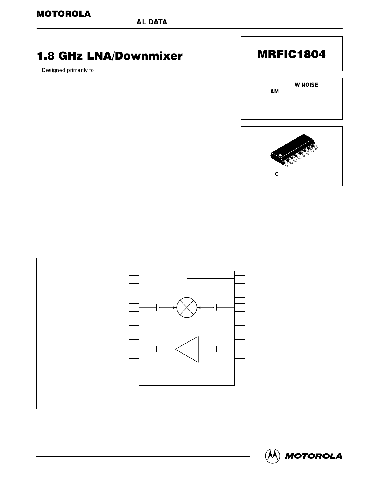
MRFIC1804 includes a low noise amplifier and downmixer in a low-cost
SOIC-16 package. The integrated circuit requires minimal off-chip matching
while allowing for the maximum in flexibility and efficiency. The mixer is
optimized for low side injection and offers reasonable intercept point as well as
high efficiency and 4 dB of conversion gain. Image filtering is implemented
off-chip to allow maximum flexibility. With both TX and RX enable pins low, the
device is in standby mode and draws less than 0.5 mA.
Together with the rest of the MRFIC180X series, this GaAs IC family offers
the complete transmit and receive functions, less LO and filters, needed for a
typical 1.8 GHz cordless telephone.
• Usable Frequency Range = 1.5 to 2.2 GHz
• 14 dB Gain, 2.3 dB Noise Figure LNA
• 4 dB Gain, 13 dB Noise Figure Mixer
• 0.9 dB Mixer Input Intercept Point
• Simple LO/IF Off-Chip Matching for Maximum Flexibility
• Low Power Consumption = 24 mW (Typ)
• Single Bias Supply = 2.7 to 3.3 V
• Low LO Power Requirement = – 5 dBm (Typ)
• Low Cost Surface Mount Plastic Package
• Available in Tape and Reel by Adding R2 Suffix to Part Number.
R2 Suffix = 2,500 Units per 16 mm, 13 inch Reel.
• Device Marking = M1804
Order this document
by MRFIC1804/D
1.8 GHz LOW NOISE
AMPLIFIER AND
DOWNMIXER
GaAs MONOLITHIC
INTEGRATED CIRCUIT
CASE 751B-05
(SO–16)
REV 2
1
V
DD
2
GND
3
RF IN
4
GND
GND
LNA OUT
GND
RX EN
5
6
7
8
MIXER
LNA
Pin Connections and Functional Block Diagram
16
15
14
13
12
11
10
9
IF OUT/V
GND
LO IN
GND
GND
LNA IN
GND
V
DD
DD
Motorola, Inc. 1995
MRFIC1804MOTOROLA RF DEVICE DATA
1
Page 2
MAXIMUM RATINGS (T
= 25°C unless otherwise noted)
A
Rating Symbol Limit Unit
Supply Voltage V
LNA Input Power (Standby Mode) LNA
LO Input Power P
Receive Enable Voltage RX EN 5 Vdc
Storage Temperature Range T
Operating Ambient Temperature T
DD
in
LO
stg
A
5 Vdc
10 dBm
0 dBm
– 65 to +150 °C
– 30 to +85 °C
RECOMMENDED OPERATING RANGES
Parameter
RF Input Frequency f
Mixer LO Frequency f
IF Output Frequency f
Supply Voltage V
Receive Enable Voltage RX EN 2.7 to 3.3 Vdc
Symbol Value Unit
RF
LO
IF
DD
1.8 to 1.925 GHz
1.5 to 1.9 GHz
70 to 325 MHz
2.7 to 3.3 Vdc
ELECTRICAL CHARACTERISTICS (V
Characteristic
LNA Gain — 14 — dB
LNA Noise Figure — 2.3 — dB
LNA Input 3rd Order Intercept — –11 — dBm
Mixer Conversion Gain (into 50 Ω) — 4 — dB
Mixer Noise Figure — 13 — dB
Mixer Input 3rd Order Intercept — 0.9 — dBm
Downconverter Gain (Less Image Filter Loss) 16 — — dB
Supply Current, RX Mode (RX EN = 3 V, LO
Standby Mode Current (RX EN = 0 V, LO off) — — 0.5 mA
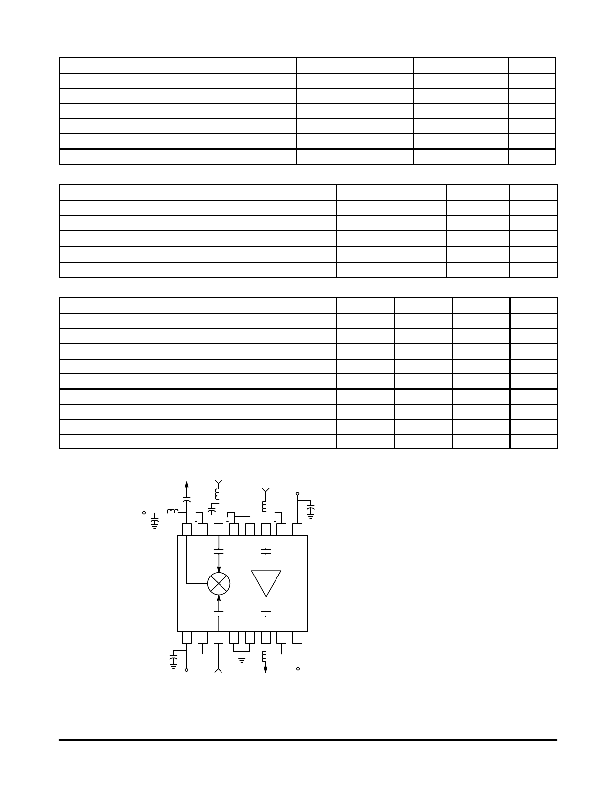
IF OUT
C1
L1
V
DD
C5
C2
15 14 13 12 11 10 9
16
12345678
= 3 V, TA = 25°C, LO = 1790 MHz @ – 5 dBm, RF = 1.9 GHz , RX EN = 3 V)
DD
Min Typ Max Unit
) — 7 10 mA
off
LO IN
L2
LNA IN
L3
V
DD
C3
C1 12 pF (110 MHz) or 7.5 pF (240 MHz)
C2 0.8 pF
C3, C4 100 pF
C5 1000 pF
L1 82 nH (110 MHz) or 15 nH (240 MHz)
L2 8.2 nH
L3, L4 3.0 nH (Microstrip)
MRFIC1804
2
LNA OUTMIXER IN
L4
RX EN
C4
V
DD
Figure 1. Applications Circuit Configuration (for 110 MHz and 240 MHz IF)
MOTOROLA RF DEVICE DATA
Page 3

S
11
S
21
S
12
S
22
Freq (GHz) Mag Angle Mag Angle Mag Angle Mag Angle
1.5 0.801 –64.71 5.65 –63.77 0.025 139.08 0.685 –62.55
1.6 0.741 –70.03 6.07 –80.96 0.033 128.21 0.622 –74.44
1.7 0.641 –73.54 6.63 –98.00 0.038 123.07 0.622 –83.36
1.8 0.559 –72.72 6.70 –113.87 0.047 113.17 0.560 –92.40
1.82 0.533 –71.10 6.58 –117.42 0.046 111.66 0.543 –93.20
1.84 0.512 –71.20 6.32 –120.25 0.046 109.36 0.530 –94.40
1.86 0.494 –69.93 5.92 –123.27 0.049 107.72 0.513 –95.19
1.88 0.478 –68.86 5.79 –126.51 0.052 106.52 0.498 –95.56
1.9 0.467 –67.50 5.88 –129.49 0.054 104.49 0.486 –96.35
1.92 0.452 –66.18 5.98 –132.33 0.055 103.55 0.476 –97.14
2.0 0.383 –57.10 5.57 –143.54 0.055 97.41 0.412 –96.10
2.1 0.326 –47.69 5.06 –155.69 0.058 92.26 0.344 –90.55
2.2 0.271 –35.10 4.61 –167.78 0.063 86.81 0.276 –83.89
2.3 0.205 –15.07 4.12 175.72 0.072 83.78 0.192 –63.78
2.4 0.708 –12.53 1.84 –155.83 0.073 45.03 0.406 –48.22
2.5 0.462 –34.07 3.18 –178.63 0.055 58.37 0.292 –66.60
T able 1. LNA S–Parameters
1.0 nH
IF OUT
500
W
15 pF
Figure 2. Equivalent IF Output Circuit
MRFIC1804MOTOROLA RF DEVICE DATA
3
Page 4

TYPICAL CHARACTERISTICS
(VDD = 3 V)
18.5
fRF = 1900 MHz
fLO = 1790 MHz
18
17.5
17
16.5
, CONVERSION GAIN (dB)
16
C
G
15.5
15
–35
5
T, TEMPERATURE (
Conversion Gain
1 dB
25 65–15 1.75 1.85 1.95
45 85
°
C)
Figure 3. Downconverter Conversion Gain (less Image
Filter) and 1 dB Compression versus T emperature
6
Conversion Gain
4
1 dB
16
0
–1
15
–2
–3
14
–4
G, GAIN (dB)
–5
1 dB COMPRESSION (dB)
13
–6
–7
12
1.7 1.9 21.8
Figure 4. LNA Gain and Noise Figure
0
6
5
–2
4
3
NF
f, FREQUENCY (GHz)
versus Frequency
Gain
2.17
2.16
2.15
2.14
2.13
NF, NOISE FIGURE (dB)
2.12
2.11
2
, CONVERSION GAIN (dB)
G
fIF = 110 MHz
fRF = 1900 MHz
C
fLO = 1790 MHz
0
– 35 –10 25 55 85 – 5
T, TEMPERATURE (°C)
Figure 5. Mixer Conversion Gain and 1 dB
–4
–6
2
, CONVERSION GAIN (dB)
C
G
1 dB COMPRESSION POINT (dBm)
1
0
–10 – 7.5 – 2.5 0
Figure 6. Mixer RF to IF Conversion Gain
Compression versus T emperature
6
5
4
3
, CONVERSION GAIN (dB)
2
C
G
fRF = fLO – IF
1
PRF = –10 dBm
0
1.7 1.85 1.9 21.75
fRF, RF FREQUENCY (GHz)
fIF = 110 MHz
240 MHz
1.951.8
–15
–17
–19
–21
–23
LO FEED THROUGH (dBm)
–25
–27
1.7
1.75
PLO, LO POWER (dBm)
versus LO Power
1.85 1.9 2
f, FREQUENCY (GHz)
fIF = 110 MHz
fRF = 1900 MHz
fLO = 1790 MHz
PRF = –10 dBm
fIF = 110 MHz
fRF = 1900 MHz
PLO = – 5 dBm
1.951.8
Figure 7. Mixer RF to IF Conversion Gain
MRFIC1804
4
versus RF Frequency
Figure 8. Mixer LO to IF Feed Through
versus RF Frequency
MOTOROLA RF DEVICE DATA
Page 5

DESIGN AND APPLICATIONS INFORMATION
The MRFIC1804 consists of a two–stage GaAs MESFET
low noise amplifier and a single ended MESFET mixer. The
LNA design conserves bias current through stacking of the
two FETs, thus reusing the current. The mixer consists of a
common gate stage driving a common source stage with
the IF output being the drain of the common source stage
shunted with 15 pF. The LNA output and mixer input have
been separated to allow the addition of an external image
filter. Such a filter, usually ceramic, is useful in improving
the mixer noise figure and third order intercept performance. It also provides LO rejection to reduce the amount
of LO power which may leak to the antenna. Alternatively,
image trapping can be implemented at the LNA input or output with discrete or distributed components.
The design has been optimized for application in the PCS
bands around 1.9 GHz but is usable from around 1.5 GHz to
2.2 GHz. For applications at 1.9 GHz and IFs of 110 MHz or
240 MHz, the circuit shown in Figure 1 can be used. This
circuit was used to derive the characterization data shown
in Figures 3 through 8. For other IF frequencies in the 100
MHz to 350 MHz range, use the IF equivalent circuit shown
in Figure 2 for matching network design. As can be seen in
the characterization curves, performance appears to degrade above about 1.85 GHz. This is partially a function of
the circuit shown in Figure 1 and can be improved, first, by
adjusting the LO input match, second, by matching LNA input and and the mixer input off chip.
As with all RF circuits, layout is important. Ground vias
must be close to the component or lead to be grounded and
vias must be plentiful. RF signal lines should be controlled
impedance such as microstrip. Bypassing of power supply
leads as shown in Figure 1 is essential to avoid oscillation of
the circuits.
EVALUATION BOARDS
Evaluation boards are available for RF Monolithic Integrated Circuits by adding a “TF” suffix to the device type.
For a complete list of currently available boards and ones
in development for newly introduced poduct, please contact your local Motorola Distributor or Sales Office.
MRFIC1804MOTOROLA RF DEVICE DATA
5
Page 6

P ACKAGE DIMENSIONS
–T–
–A–
16 9
–B–
18
8 PLP
0.25 (0.010) B
G
K
C
SEATING
PLANE
D
16 PL
0.25 (0.010) A
M
S
B
T
M
S
CASE 751B–05
M
R
X 45
ISSUE J
NOTES:
1. DIMENSIONING AND TOLERANCING PER ANSI
Y14.5M, 1982.
2. CONTROLLING DIMENSION: MILLIMETER.
3. DIMENSIONS A AND B DO NOT INCLUDE
MOLD PROTRUSION.
4. MAXIMUM MOLD PROTRUSION 0.15 (0.006)
PER SIDE.
S
_
F
J
5. DIMENSION D DOES NOT INCLUDE DAMBAR
PROTRUSION. ALLOWABLE DAMBAR
PROTRUSION SHALL BE 0.127 (0.005) TOTAL
IN EXCESS OF THE D DIMENSION AT
MAXIMUM MATERIAL CONDITION.
DIM MIN MAX MIN MAX
A 9.80 10.00 0.386 0.393
B 3.80 4.00 0.150 0.157
C 1.35 1.75 0.054 0.068
D 0.35 0.49 0.014 0.019
F 0.40 1.25 0.016 0.049
G 1.27 BSC 0.050 BSC
J 0.19 0.25 0.008 0.009
K 0.10 0.25 0.004 0.009
M 0 7 0 7
____
P 5.80 6.20 0.229 0.244
R 0.25 0.50 0.010 0.019
INCHESMILLIMETERS
Motorola reserves the right to make changes without further notice to any products herein. Motorola makes no warranty, representation or guarantee regarding
the suitability of its products for any particular purpose, nor does Motorola assume any liability arising out of the application or use of any product or circuit,
and specifically disclaims any and all liability, including without limitation consequential or incidental damages. “T ypical” parameters can and do vary in different
applications. All operating parameters, including “T ypicals” must be validated for each customer application by customer’s technical experts. Motorola does
not convey any license under its patent rights nor the rights of others. Motorola products are not designed, intended, or authorized for use as components in
systems intended for surgical implant into the body, or other applications intended to support or sustain life, or for any other application in which the failure of
the Motorola product could create a situation where personal injury or death may occur. Should Buyer purchase or use Motorola products for any such
unintended or unauthorized application, Buyer shall indemnify and hold Motorola and its officers, employees, subsidiaries, affiliates, and distributors harmless
against all claims, costs, damages, and expenses, and reasonable attorney fees arising out of, directly or indirectly, any claim of personal injury or death
associated with such unintended or unauthorized use, even if such claim alleges that Motorola was negligent regarding the design or manufacture of the part.
Motorola and are registered trademarks of Motorola, Inc. Motorola, Inc. is an Equal Opportunity/Af firmative Action Employer.
How to reach us:
USA/ EUROPE: Motorola Literature Distribution; JAPAN: Nippon Motorola Ltd.; Tatsumi–SPD–JLDC, Toshikatsu Otsuki,
P.O. Box 20912; Phoenix, Arizona 85036. 1–800–441–2447 6F Seibu–Butsuryu–Center, 3–14–2 Tatsumi Koto–Ku, Tokyo 135, Japan. 03–3521–8315
MFAX: RMF AX0@email.sps.mot.com – T OUCHTONE (602) 244–6609 HONG KONG: Motorola Semiconductors H.K. Ltd.; 8B Tai Ping Industrial Park,
INTERNET: http://Design–NET.com 51 Ting K ok Road, T ai Po, N.T., Hong Kong. 852–26629298
MRFIC1804
6
◊
MOTOROLA RF DEVICE DATA
*MRFIC1804/D*
MRFIC1804/D
 Loading...