

Page 1
SEMICONDUCTOR TECHNICAL DATA
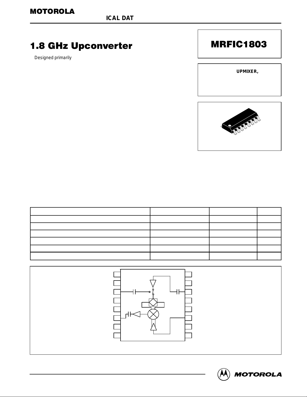
The MRFIC Line
Designed primarily for use in DECT , Japan’ s Personal Handy System (PHS),
and other wireless Personal Communication Systems (PCS) applications at 1.8
GHz, but also applicable to Industrial, Scientific and Medical (ISM) applications
at 2.5 GHz. The MRFIC1803 is a complete active upmixer, exciter amplifier , and
LO buffer amplifier in a low-cost SOIC-16 package. The low power consumption
design includes a single balanced active mixer, CMOS compatible receive and
transmit enable inputs, a buffer/exciter amplifier, and a buffered LO output
capable of driving the MRFIC1804 downconverter. IF, LO and RF ports are
matched to 50 Ω and no off-chip baluns are required. With both TX and RX
enable pins low, the device is in standby mode and draws less than 0.3 mA.
Together with the rest of the MRFIC180X series, this GaAs IC family offers
the complete transmit and receive functions, less LO and filters, needed for a
typical 1.8 GHz cordless telephone.
• 10 dB IF to RF Conversion Gain
• Usable Frequency Range = 1.7 to 2.5 GHz
• Low Power Consumption = 80 mW (Typ)
• Single Bias Supply = 2.7 to 3.3 V
• No External Baluns Required
• IF, LO and RF Ports Matched to 50 Ω
• Low LO Power Requirement = –10 dBm (Typ)
• Low Cost Surface Mount Plastic Package
• Order MRFIC1803R2 for Tape and Reel.
R2 Suffix = 2,500 Units per 16 mm, 13 inch Reel.
• Device Marking = M1803
Order this document
by MRFIC1803/D
1.8 GHz UPMIXER,
EXCITER AND LO AMP
GaAs MONOLITHIC
INTEGRATED CIRCUIT
CASE 751B-05
(SO–16)
MAXIMUM RATINGS
(TA = 25°C unless otherwise noted)
Ratings Symbol Value Unit
Supply Voltage V
IF Input Power P
LO Input Power P
Transmit and Receive Enable V oltage
Storage Temperature Range T
Operating Ambient Temperature T
1GND
GND
LO OUT
GND
GND
RF OUT
GND
V
DD
LO BUFFER
2
AND SWITCH
3
4
EXCITER
5
6
ACTIVE
7
BALANCED
MIXER
8
TX EN, RX EN 5.5
DD
IF
LO
stg
A
16
15
14
13
12
11
10
9
5.5 Vdc
3 dBm
3 dBm
Vdc
– 65 to +150 °C
– 30 to + 85 °C
RX EN
GND
LO IN
GND
GND
IF IN
GND
TX EN
REV 3
Motorola, Inc. 1997
Pin Connections and Functional Block Diagram
MRFIC1803MOTOROLA RF DEVICE DATA
1
Page 2
RECOMMENDED OPERATING RANGES
Parameter
LO Input Frequency f
LO Input Power P
IF Input Frequency f
RF Output Frequency f
Transmit and Receive Enable V oltage TX EN, RX EN 2.7 to V
Supply Voltage V
Symbol Value Unit
LO
LO
IF
RF
DD
1.5 to 2.4 GHz
70 to 350 MHz
1.7 to 2.5 GHz
2.7 to 5 Vdc
–10 dBm
DD
Vdc
ELECTRICAL CHARACTERISTICS (V
TX EN = 3.0 V, RX EN = 0 V, unless otherwise noted)
Characteristic
IF to RF Conversion Gain 8 10 — dB
RF Output 1 dB Compression — –2 — dBm
RF Output 3rd Order Intercept — 9 — dBm
LO Feed Through to RF Port — –19 — dBm
Auxiliary LO Output Power (TX EN = 0 V, RX EN = 3 Vdc) — –4 — dBm
Supply Current, TX Mode — 28 50 mA
Supply Current, RX Mode (TX EN = 0 V, RX EN = 3 Vdc) — 3 — mA
Standby Mode Current (TX EN = 0 V, RX EN = 0 Vdc) — 0.1 0.3 mA
= 3 V, TA = 25°C, LO = 1790 MHz @ –10 dBm, IF = 110 MHz @ –15 dBm,
DD
Min Typ Max Unit
RX EN LO IN IF IN TX EN
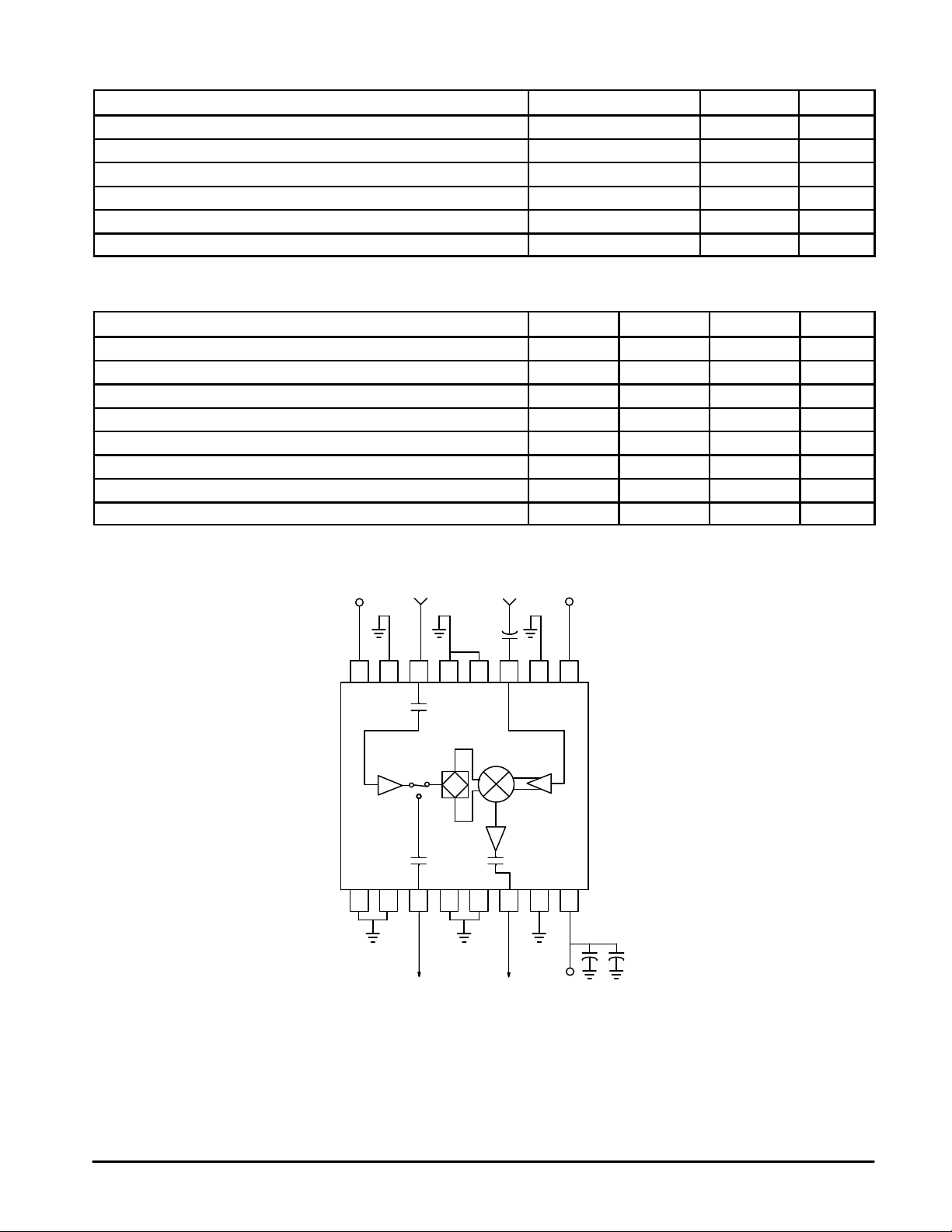
C1
15
1416
10 9111213
MRFIC1803
2
1
2
345678
LO OUT RF OUT V
C1 470 pF
C2 100 pF
C3 0.1 µF (optional)
DD
Figure 1. Applications Circuit Configuration
C2
C3
MOTOROLA RF DEVICE DATA
Page 3

T ypical Characteristics
ÎÎÎ
13
12
11
10
9
8
7
6
GC, CONVERSION GAIN (dB)
5
4
3
–15 –13 –11 –9 –7 –5
VDD = 3.0 Vdc
2.7 Vdc
3.3 Vdc
fRF = 1.9GHz
PIF = –20dBm
fIF = 110MHz
TA = 25°C
PLO, LO INPUT POWER (dBm)
Figure 2. Conversion Gain versus LO Power
14
12
10
8
6
4
2
0
GC,CONVERSION GAIN (dB)
–2
–4
1.5 1.6 1.7 1.8 1.9 2 2.1 2.2 2.3 2.4 2.5 2.6
–35°C
TA = 25°C
fIF = 110 MHz
PRF = –20 dBm
PLO = –10 dBm
VDD = 3 Vdc
fRF, RF FREQUENCY (GHz)
85
°
C
14
12
10
8
GC,CONVERSION GAIN (dB)
6
4
–15 –13 –11 –9 –7 –5
PLO, LO INPUT POWER (dBm)
–35°C
TA = 25°C
°
C
85
fRF = 1.9 GHz
PIF = –20 dBm
fIF = 110 MHz
VDD = 3 Vdc
Figure 3. Conversion Gain versus LO Power
13
11
9
7
5
3
1
–1
GC,CONVERSION GAIN (dB)
–3
–5
1.5 1.6 1.7 1.8 1.9 2 2.1 2.2 2.3 2.4 2.5
fIF = 110 MHz
PIF = –20 dBm
PLO = –10 dBm
TA = 25
3.3 Vdc
°
C
fRF, RF FREQUENCY (GHz)
2.7 Vdc
VDD = 3.0 Vdc
2.6
Figure 4. Conversion Gain versus RF Frequency Figure 5. Conversion Gain versus RF Frequency
12
10
8
6
4
GC,CONVERSION GAIN (dB)
2
0
1.5 1.6 1.7 1.8 1.9 2 2.1 2.2 2.3 2.4 2.5 2.6
IF = 240 MHz
PIF = –20 dBm
PLO = –10 dBm
VDD = 3 Vdc
°
C
TA = 25
fRF, RF FREQUENCY (GHz)
110 MHz
325 MHz
5
4
3
2
1
0
–1
–2
–3
–4
–5
–6
–7
RF
PRF, RF OUTPUT POWER (dBm)
–8
–9
–10
–11
–20 –15 –10 –5 0
VDD = 3 Vdc
2.7 Vdc
fRF = 1.9 GHz
fIF = 110 MHz
3.3 Vdc
PIF, IF INPUT POWER (dBm)
PLO = –10 dBm
TA = 25
Figure 6. Conversion Gain versus RF Frequency Figure 7. RF Output Power versus IF Input Power
°
C
MRFIC1803MOTOROLA RF DEVICE DATA
3
Page 4

T ypical Characteristics
6
4
2
0
–2
–4
–6
–8
RF
PRF, RF OUTPUT POWER (dBm)
–10
–12
–20 –15 –10 –5 0
–35°C
°
C
85
TA = 25°C
PIF, IF INPUT POWER (dBm)
fIF = 110 MHz
fRF = 1.9 GHz
VDD = 3 Vdc
Figure 8. RF Output Power versus IF Input Power
4
2
0
–2
–4
–6
–8
–10
RF
PRF, RF OUTPUT POWER (dBm)
–12
–14
–16
–20 –15 –10 –5 0
PIF, IF INPUT POWER (dBm)
325 MHz
IF = 110 MHz
fRF = 2.45 GHz
VDD = 3 Vdc
TA = 25
240 MHz
°
C
Figure 10. RF Output Power versus IF Input
Power at 2.45GHz
6
4
2
0
–2
–4
–6
RF
PRF, RF OUTPUT POWER (dBm)
–8
–10
–20 –15 –10 –5 0
240 MHz
IF = 110 MHz
PIF, IF INPUT POWER (dBm)
325 MHz
fRF = 1.9 GHz
VDD = 3 Vdc
°
TA = 25
Figure 9. RF Output Pwer versus IF Input Power
0
–5
–10
–15
–20
PRF = –20 dBm
LO–RF FEEDTHROUGH (dBm)
PLO = –10 dBm
–25
VDD = 3 Vdc
°
C
TA = 25
–30
1 1.2 1.4 1.6 1.8
fLO, LO FREQUENCY (GHz)
Figure 11. LO to RF Feedthrough versus
240 MHz
2
IF = 110 MHz
325 MHz
2.2 2.4 2.6
LO Frequency
C
MRFIC1803
4
MOTOROLA RF DEVICE DATA
Page 5

Frequency (MHz) RF Output LO Input LO Output
1500 22.07 –j11.36 41.98 +j22.31 20.09 +j31.15
1550 21.74 –j4.69 50.60 +j9.80 26.39 +j40.79
1600 22.28 +j2.16 41.93 –j0.07 37.63 +j52.47
1650 24.01 +j8.25 32.74 +j3.32 56.16 +j63.47
1700 26.64 +J14.13 28.78 +j11.39 87.97 +j67.31
1750 30.83 +j20.1 1 28.98 +j21.04 131.33 +j40.34
1800 36.39 +j25.30 32.13 +j30.26 137.85 –j16.48
1850 43.92 +j29.26 37.68 +j40.38 103.88 –j50.81
1900 54.37 +j30.98 48.31 +j54.15 69.58 –j53.97
1950 65.34 +j28.57 68.80 +j70.87 50.13 –j46.24
2000 75.30 +j21.12 118.18 +j86.46 38.97 –j36.86
2050 81.19 +j8.43 220.83 +j17.19 32.08 –j27.58
2100 80.22 –j4.24 148.91 –j120.77 28.43 –j19.86
2150 74.20 –j14.00 58.50 –j105.11 26.56 –j12.82
2200 65.50 –j19.72 27.23 –j71.51 26.03 –j5.89
2250 57.40 –j21.38 17.22 –j50.26 26.73 –j0.03
2300 50.59 –j20.61 13.00 –j35.19 28.46 +j5.10
2350 44.53 –j18.16 10.95 –j22.96 30.88 +j9.86
2400 40.24 –j14.78 10.23 –j13.58 33.75 +j13.92
2450 37.73 –j10.54 10.20 –j5.32 37.50 +j17.32
2500 36.38 –j6.72 10.62 +j2.90 42.00 +j20.34
T able 1. Selected Device Impedances
DESIGN AND APPLICATIONS INFORMATION
The MRFIC1803 combines a single–balanced FET mixer with an LO pre–amp and an exciter amplifier to form a
self–contained upconverter. The device is usable from RF
frequencies of 1.7 to 2.5 GHz and at IF frequencies of 70
to 325 MHz. The design is optimized for low side injection
in hetrodyne transmitter applications. In the upconversion
process, modulation is imparted to an IF carrier which is
converted to the RF transmit frequency by a mixer. By DC
coupling the IF input, the device can be used for simple
on–off keying (OOK) or bi–phase shift keying (BPSK) applications with no IF.
The MRFIC1803 design minimizes the need for off–chip
components. An active balun is employed at the IF input
and provides an excellent broadband 50 match over the
full range of IF frequencies. The LO quadrature divider is
passive and internal to the device. The LO buffer amplifier
is equipped with a diversity switch which switches the amplified LO signal to the LO output pin during RECEIVE
mode. The –5 dBm LO output is the appropriate level to
drive the MRFIC1804 for 1.8 GHz applications or the
MRFIC2401 for 2.4 GHz applications.
As shown in Figure 1, the device is easy to use with
minimal off–chip components. More or les s bypassing of
the control and supply lines may be required depending
on board layout and shielding. Careful layout of the RF
frequency portions of the board is critical to successful
implementation. Controlled impedance lines must be used
and any off–chip components must be mounted as close to
the IC as possible. The applications circuit was used to
gather the information displayed in the typical characteristics curves. Since the MRFIC1803 design was optimized
for the 1.7 to 1.9 GHz frequency range, improved performance can be had with some off–chip matching at frequencies outside this range. In particular , matching of the
LO port will supply higher LO drive and improve conversion gain. At the RF output, either better gain or better 1dB
compression can be had with external matching.
Filtering is generally required in the upconversion process to reduce image and LO radiation. To minimize pin
count, this filtering is accomplished external to the device
at the exciter output. For the frequency ranges of application, two and three pole ceramic surface filters are available at reasonable cost and with less than 2 dB of loss.
EVALUATION BOARDS
Evaluation boards are available for RF Monolithic Integrated Circuits by adding a “TF” suffix to the device type.
For a complete list of currently available boards and ones
in development for newly introduced product, please con tact your local Motorola Distributor or Sales Office.
MRFIC1803MOTOROLA RF DEVICE DATA
5
Page 6

P ACKAGE DIMENSIONS
–T–
–A–
16 9
–B–
18
8 PLP
0.25 (0.010) B
G
K
C
SEATING
PLANE
D
16 PL
0.25 (0.010) A
M
S
B
T
M
S
CASE 751B–05
M
R
X 45
_
ISSUE J
NOTES:
1. DIMENSIONING AND TOLERANCING PER ANSI
Y14.5M, 1982.
2. CONTROLLING DIMENSION: MILLIMETER.
3. DIMENSIONS A AND B DO NOT INCLUDE
MOLD PROTRUSION.
4. MAXIMUM MOLD PROTRUSION 0.15 (0.006)
PER SIDE.
S
F
J
5. DIMENSION D DOES NOT INCLUDE DAMBAR
PROTRUSION. ALLOWABLE DAMBAR
PROTRUSION SHALL BE 0.127 (0.005) TOTAL
IN EXCESS OF THE D DIMENSION AT
MAXIMUM MATERIAL CONDITION.
DIM MIN MAX MIN MAX
A 9.80 10.00 0.386 0.393
B 3.80 4.00 0.150 0.157
C 1.35 1.75 0.054 0.068
D 0.35 0.49 0.014 0.019
F 0.40 1.25 0.016 0.049
G 1.27 BSC 0.050 BSC
J 0.19 0.25 0.008 0.009
K 0.10 0.25 0.004 0.009
M 0 7 0 7
____
P 5.80 6.20 0.229 0.244
R 0.25 0.50 0.010 0.019
INCHESMILLIMETERS
Motorola reserves the right to make changes without further notice to any products herein. Motorola makes no warranty , representation or guarantee regarding
the suitability of its products for any particular purpose, nor does Motorola assume any liability arising out of the application or use of any product or circuit, and
specifically disclaims any and all liability, including without limitation consequential or incidental damages. “T ypical” parameters which may be provided in Motorola
data sheets and/or specifications can and do vary in different applications and actual performance may vary over time. All operating parameters, including “Typicals”
must be validated for each customer application by customer’s technical experts. Motorola does not convey any license under its patent rights nor the rights of
others. Motorola products are not designed, intended, or authorized for use as components in systems intended for surgical implant into the body, or other
applications intended to support or sustain life, or for any other application in which the failure of the Motorola product could create a situation where personal injury
or death may occur. Should Buyer purchase or use Motorola products for any such unintended or unauthorized application, Buyer shall indemnify and hold Motorola
and its officers, employees, subsidiaries, affiliates, and distributors harmless against all claims, costs, damages, and expenses, and reasonable attorney fees
arising out of, directly or indirectly, any claim of personal injury or death associated with such unintended or unauthorized use, even if such claim alleges that
Motorola was negligent regarding the design or manufacture of the part. Motorola and are registered trademarks of Motorola, Inc. Motorola, Inc. is an Equal
Opportunity/Affirmative Action Employer.
Mfax is a trademark of Motorola, Inc.
How to reach us:
USA/EUROPE/Locations Not Listed: Motorola Literature Distribution; JAPAN: Nippon Motorola Ltd.: SPD, Strategic Planning Office, 4–32–1,
P.O. Box 5405, Denver, Colorado 80217. 303–675–2140 or 1–800–441–2447 Nishi–Gotanda, Shinagawa–ku, Tokyo 141, Japan. 81–3–5487–8488
Mfax: RMFAX0@email.sps.mot.com – TOUCHTONE 602–244–6609 ASIA/PACIFIC: Motorola Semiconductors H.K. Ltd.; 8B Tai Ping Industrial Park,
– US & Canada ONLY 1–800–774–1848 51 Ting Kok Road, T ai Po, N.T., Hong Kong. 852–26629298
INTERNET: http://motorola.com/sps
MRFIC1803
◊
MOTOROLA RF DEVICE DATA
MRFIC1803/D
6
 Loading...