

Page 1
SEMICONDUCTOR TECHNICAL DATA
The MRFIC Line
This integrated circuit is intended for GPS receiver applications. The dual
conversion design is implemented in Motorola’s low–cost high performance
MOSAIC 3 silicon bipolar process and is packaged in a low–cost surface mount
TQFP–48 package. In addition to the mixers, a VCO, a PLL and a loop filter are
integrated on–chip. Output IF is nominally 9.5 MHz.
• 65 dB Minimum Conversion Gain
• 5 Volts Operation
• 50 mA Typical Current Consumption
• Low–Cost, Low Profile Plastic TQFP Package
• Device Marking = M1502
GND GND GND GND RF IN GND V
48 47 46 45 44 43 42 41 40 39 38 37
CC1
GND
BPF
TO
FROM
BPF
Order this document
by MRFIC1502/D
1.575 GHz GPS
DOWNCONVERTER
CASE 932–02
(TQFP–48)
GND GND
GND
VCO VT
GND
V
CC5
GND
VCO CE
GND
SF CAP1
GND
SF CAP2
GND
GND
TQFP–48
1
2
3
4
5
6
7
8
9
10
11
12
ACTIVE
FILTER
LOOP
FILTER
13 14 15 16 17 18 19
C2A C2B C1 CA CB DCX0 V
VCO
40
PHASE
DETECTOR
20 21 22 23
GND CLK
CC4
2
OUT
GND GND
24
GND
GND
36
35
38 MHz TRAP
38 MHz TRAP
34
33
BYPASS CAP
32
IF OUT
31
V
CC2
GND
30
GAIN CONTROL
29
V
28
CC3
GND
27
GND
26
GND
25
Motorola, Inc. 1997
MOTOROLA RF DEVICE DATA
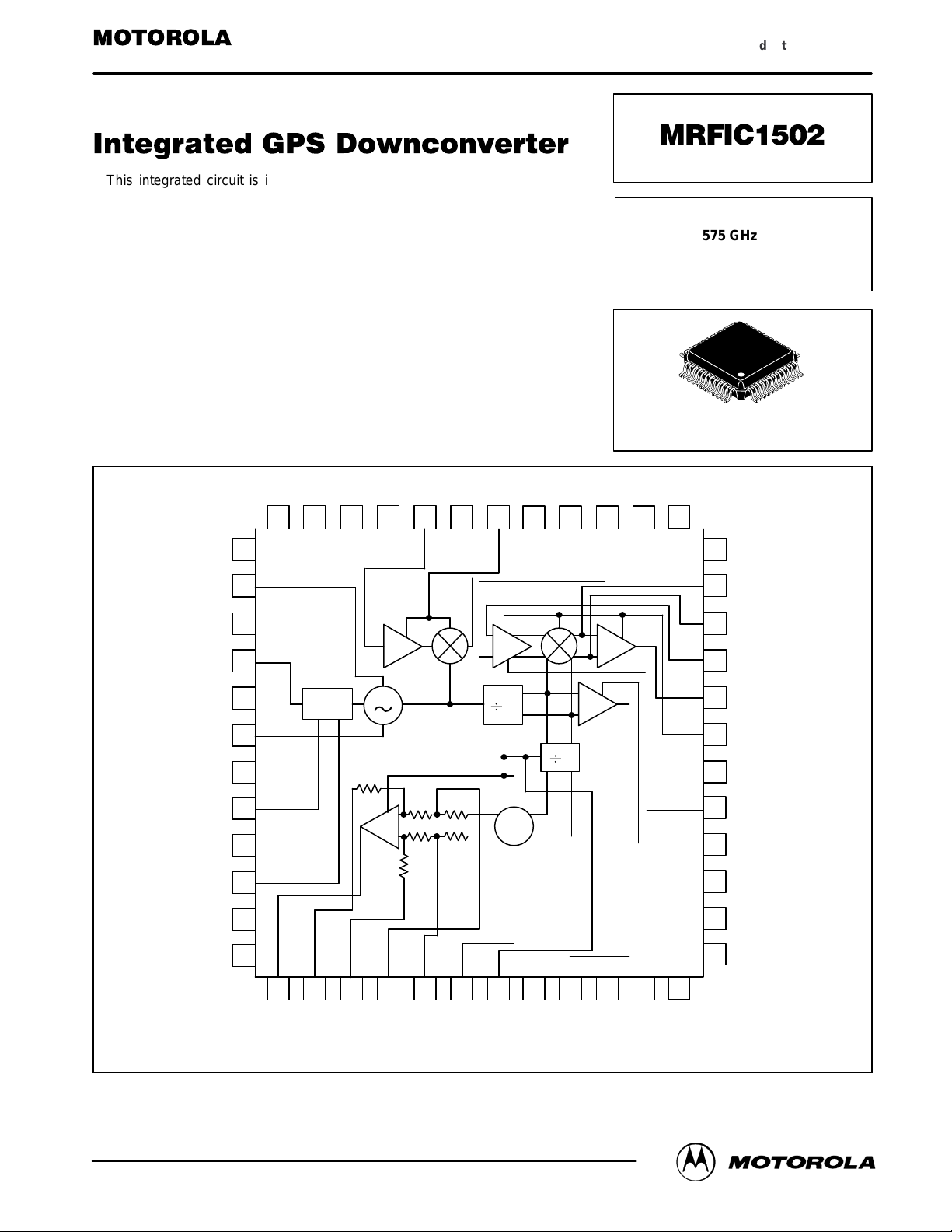
Pin Connections and Functional Block Diagram
MRFIC1502
1
Page 2
MAXIMUM RATINGS
Rating Symbol Limit Unit
DC Supply Voltage V
DC Supply Current I
Operating Ambient Temperature T
Storage Temperature Range T
Lead Soldering Temperature Range (10 seconds) — +260 °C
DD
DD
A
stg
+6.0 Vdc
60 mA
– 40 to +100 °C
– 65 to +150 °C
ELECTRICAL CHARACTERISTICS (T
Characteristic
Supply Voltage 4.75 — 5.25 Vdc
Supply Current — — 60 mA
L–Band Gain (Measured from L–Band Input to 47 MHz Output) — 20 — dB
IF Gain (Measured from 47 MHz Input to 9.5 MHz Output with Gain
Control at Maximum)
Conversion Gain (Measured from L–Band Input to 9.5 MHz Output with
Gain Control at Maximum)
Gain Control (Externally Adjustable 0 to 5.0 V , Maximum at 0 V) — 40 — dB
Noise Figure (Double Sideband) — 9.5 — dB
L–Band Input VSWR (Measured into 50 Ω; 1575.42 ± 5.0 MHz) — 2:1 — —
First IF Output VSWR (Measured into 50 Ω; 47.74 ± 5.0 MHz) — 2:1 — —
Second IF Output VSWR (Measured into 50 Ω; 9.5 ± 5.0 MHz) — 2:1 — —
Input Impedance @ 1st IF 47.7 ± 5 MHz (For Reference Only) — 2000 — Ω
Output 1.0 dB Compression Point — –7 — dBm
First LO (Measured at the First IF Output) — –20 — dBm
All Other Harmonics (Measured at the First IF Output) — –45 — dBm
38.1915 MHz Leakage at First IF Output — –50 — dBm
Second LO (Measured at the Second IF Output) — –25 — dBm
All Other Harmonics (Measured at Second IF Output) — –45 — dBm
Reference Oscillator Input 400 — 4500 mVpp
Clock Output
Frequency
Amplitude
Low
HIgh
(Clock Amplitude Measured with the Output Loaded in 15 pF and 40 kΩ)
Duty Cycle
VCO Lock Voltage 1.2 — 3.0 V
Phase Detector Gain — 0.16 — V/Radian
VCO Modulation Sensitivity — 15 — MHz/V
= 25°C, and VCC = 5 V, Tested in Circuit shown in Figure 1 unless otherwise noted)
A
Min Typ Max Unit
— 45 — dB
65 — — dB
2Xf
ref
—
2.0
45
— 2Xf
ref
0.8
—
55
V
V
%
MRFIC1502
2
MOTOROLA RF DEVICE DATA
Page 3
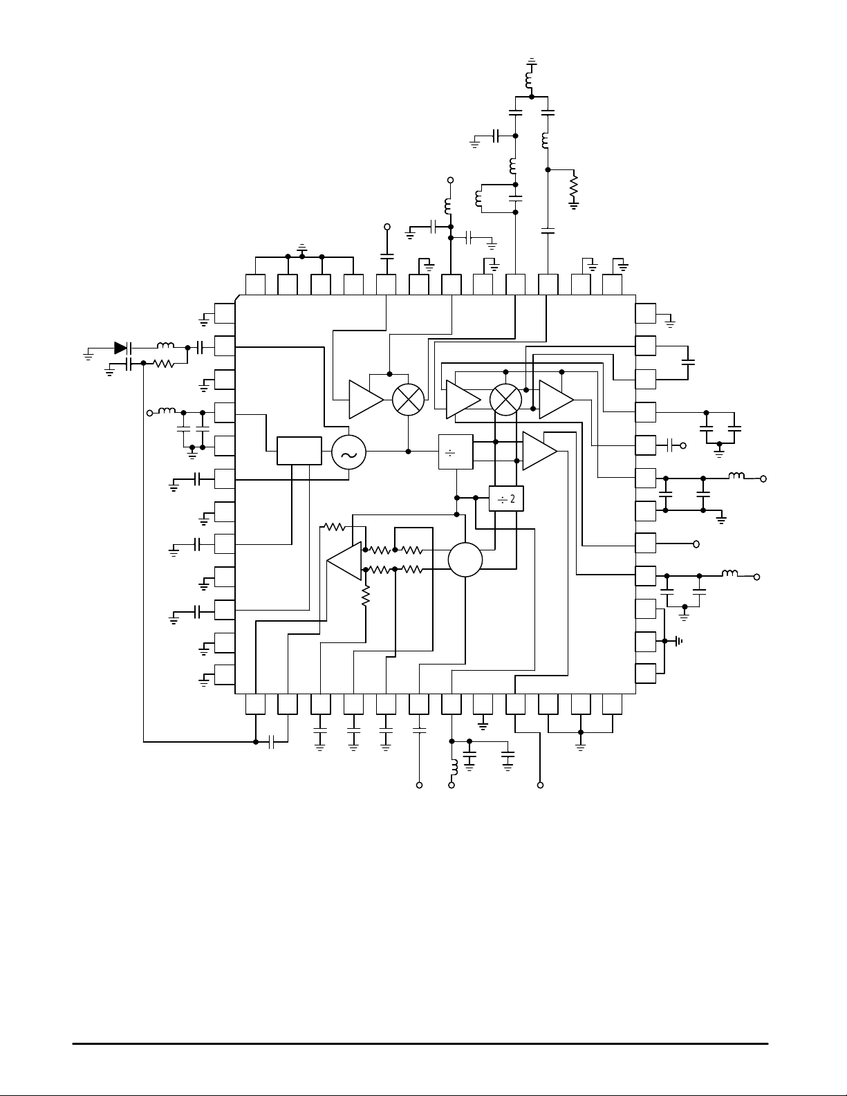
L7
C21C22
CR1
C31
C23
V
CC
RF
INPUT
C18
48 47 46 45 44 43 42
TQFP–48
1
C17
L3
R1
V
CC
L1
C15
C35
C16
2
3
4
5
6
7
ACTIVE
FILTER
VCO
L10
C19
40
L8
L9
C24
C34
41 40 39 38
2
L6
C20
R3
37
36
35
34
33
C12
32
IF OUTPUT
31
C10 C1 1
30
C14
C36 C13
V
L5
CC
8
C3
10
C2
11
12
C1, C8, C10, C12, C13, C15,
C19, C20, C37 10,000 pF
C4, C5 5600 pF
C6, C7, C31 1000 pF
C2, C3 1.0 µF
C14 3.9 pF, ATC
C16, C18, C36 27 pF, ATC
C17 15 pF, ATC
C21 5.6 pF, ATC
C9, C11, C34, C36 47 pF, ATC
C22, C23 120 pF, A TC
LOOP
9
FILTER
13 14 15 16 17 18 19
C5 C6 C7 C1
C4
29
PHASE
DETECTOR
20 21 22 23
L1
DXCO
C36 C37
V
CC
C24 68 pF, ATC
C35 0.4 pF, ATC
CR1 2.7 pF , MA45233–123, MACOM
L1, L4, L5, L10 2.2 µH, 1008CS–222XKBC, COILCRAFT
L3 2.2 nH, LL2012–F2N2S, TOKO
L6 2.2 µH
L7 220 nH
L8 0.56 µH
L9 0.27 µH
R1 10 kΩ
R3 220 Ω
CLOCK
OUTPUT
28
27
26
25
24
GAIN CONTROL
C8 C9
L4
V
CC
MOTOROLA RF DEVICE DATA
Figure 1. T est Circuit Configuration
MRFIC1502
3
Page 4

T able 1. Port Impedance Derived from Circuit Characterization
f
Pin Number Pin Name
44 RF IN 1575.42 38.3 –16.09
40 TO BPF 47.74 54.45 11.3
39 FROM BPF 47.74 43 1.5
32 IF OUT 9.5 560 –850
Zin represents the input impedance of the pin.
APPLICATION INFORMATION
Design Philosophy
The MRFIC1502 design is a standard dual downconversion configuration with an integrated fixed frequency phase–
locked loop to generate the two local oscillators and the
buffer to generate the sampling clock for a digital correlator
and decimator. The active device for the L–band VCO is also
integrated on the chip. This chip is designed in the third
generation of Motorola’s Oxide Self Aligned Integrated
Circuits (MOSAIC 3) silicon bipolar process.
Circuit Considerations
The RF input to the MRFIC1502 is internally matched to 50
ohms. Therefore, only AC coupling is required on the input.
The output of the amplifier is fed directly into the first mixer.
This mixer is an active Gilbert Cell configuration. The output
of the mixer is brought off–chip for filtering of the unwanted
mixer products. The amplifier and mixer have their own V
supply (pin 42) in order to reduce the amount of coupling to
the other circuits. There are two bypass capacitors on this
pin, one for the high frequency components and one for the
lower frequency components. These two capacitors should
be placed physically as close to the bias pin as possible to
reduce the inductance in the path. The capacitors should
also be grounded as close to the ground of the IC as
possible, preferably through a ground plane.
The output impedance of the first mixer is 50 ohms, while
the input impedance to the first IF amplifier is 1 kΩ. There is
a trap (zero) designed in at the second LO frequency to limit
the amount of LO leakage into the high gain first IF amplifier.
The first IF amplifier is a variable gain amplifier with 25 dB
of gain and 40 dB of gain control. The gain control pin can be
grounded to provide the maximum gain out of the amplifier. If
the baseband design utilizes a multi–bit A/D converter in the
digital signal processing chip, this amplifier could be used to
control the input to the A/D converter. The amplifier has an
external bypassing capacitor. This capacitor should be on the
order of 0.01 µF, and again should be located near the
package pin.
The second mixer design is also a Gilbert Cell configuration. The interface between the mixer and the second IF
amplifier is differential in order to increase noise immunity.
This differential interface is also brought off–chip so that
some additional filtering could be added in parallel between
CC
Z
in
f
(MHz)
Ohms
R jX
the output of the mixer and input to the amplifier. This filtering
is primarily to reduce the amount of LO leakage into the final
IF amplifier and is achieved using a single 3.9 pF capacitor
across the differential ports. The value of the capacitor
determines the high frequency of the low pass structure.
The supply pin for the IF circuits is pin 33. This supply pin
should be isolated from the other chip supplies in order to
reduce the amount of coupling. The recommended capacitors are a 47 pF and a 0.01 µF, in parallel to bypass the
supply to ground and should be placed physically as close to
the pin as possible.
The output of the second IF amplifier is 50 ohms with a
bandwidth of ±5.0 MHz. This signal must be filtered before
being digitized in order to limit the noise entering the A/D
converter.
VCO Resonator Design
The design and layout of the circuits around the voltage
controlled oscillator (VCO) are the most sensitive of the
entire layout. The active device and biasing resistors are
integrated on the MRFIC1502. The external circuits consist
of the power supply decoupling, the capacitors for the
integrated supply superfilter, the resonator and frequency
adjusting elements, and the bypassing capacitor on the
emitter of the active device.
The VCO supply is isolated from the rest of the PLL circuits
in order to reduce the amount of noise that could cause
frequency/phase noise in the VCO. The supply should be
filtered using a 22 µH inductor in series and a 27 pF and
0.01 µF in parallel. The 27 pF capacitor should be series
resonant at least as high as the VCO frequency to get the
most L–band bypassing as possible. The on–chip supply
filter requires two capacitors off–chip to filter the supply. The
capacitors on the input (pin 8) and output (pin 10) of the filter
are 1.0 µF, and the output also has a high frequency bypass
capacitor in parallel. The input capacitor should not be smaller
than a 1.0 µF to insure stability of the supply filter.
The VCO design is a standard negative resistance cell with
a buffer amplifier. The resonating structure is connected to
the base of the active device and consists of a coupling
capacitor, a hyper–abrupt varactor diode, and a wire wound
chip inductor. With the values shown on the application
MRFIC1502
4
MOTOROLA RF DEVICE DATA
Page 5

circuit, the VCO is centered at 1527.7 MHz, and the gain of
the VCO is approximately 20 MHz/Volt.
The above performance is heavily dependent on the
capacitive structure that is used as the emitter bypass on pin
6. The total capacitance should be approximately 1.0 pF; that
can be achieved using either a discrete element or a
microstrip open circuited stub. The evaluation circuit shown
uses a 0.4 pF capacitor.
Phase–locked Loop Design
The VCO signal at 1527.68 MHz is divided by 40 to get the
second LO frequency of 38.19 MHz. In addition to providing
the LO to the second mixer, the 38 MHz signal is output
through a translator and is used as the sampling clock for the
digital correlator and decimator circuits. There is an additional divide by two so the signal used by the phase detector is at
19.096 MHz. The r e f er e n c e i nput to the phase detector (pin 18)
has an input sensitivity of 400 mVpp minimum and 2.5 Vpp
maximum.
The loop filter design is the standard op–amp loop filter,
resulting in a type 2 second order loop. The layout of the
discrete components around the loop filter and VCO is very
critical to the performance of the phase–locked loop. Care
should be taken in routing the VCO control voltage line from
the output of the loop filter to the varactor diode.
The output of the divide by 40 is buffered by a clock
translator that converts the low level sine wave into a TTL
level square wave. The loading on the buffer is high so the
peak currents can reach as high as 50 mA with the maximum
load of 1.0 kΩ in parallel with 40 pF on the output. Therefore,
the translator has a dedicated VCC supply, pin 28, which
requires external bypassing and isolation. The recommended bypassing uses two capacitors in parallel, a 47 pF
and a 0.01 µF capacitor.
Conclusion
The MRFIC1502 offers a highly integrated downconverter
solution for GPS receivers. For more detailed applications
information on GPS system design refer to application note
AN1610, “Using Motorola’s MRFIC1502 in Global Positioning
System Receivers.”
MOTOROLA RF DEVICE DATA
MRFIC1502
5
Page 6

P ACKAGE DIMENSIONS
B
B1
–AB–
–AC–
9
–T–
4X
Z0.200 (0.008) AB T–U
–U–
DETAIL Y
P
A
A1
48
1
37
36
V
AE AE
12
13
24
V1
25
–Z–
S1
–T–, –U–, –Z–
S
4X
DETAIL Y
Z0.200 (0.008) AC T–U
G
0.080 (0.003) AC
AD
_
BASE METAL
M
TOP & BOTTOM
NOTES:
1.DIMENSIONING AND TOLERANCING PER ANSI
Y14.5M, 1982.
2. CONTROLLING DIMENSION: MILLIMETER.
3.DATUM PLANE –AB– IS LOCATED AT BOTTOM
OF LEAD AND IS COINCIDENT WITH THE LEAD
WHERE THE LEAD EXITS THE PLASTIC BODY AT
THE BOTTOM OF THE PARTING LINE.
4.DA TUMS –T–, –U–, AND –Z– TO BE DETERMINED
AT DATUM PLANE –AB–.
5.DIMENSIONS S AND V TO BE DETERMINED AT
SEATING PLANE –AC–.
6.DIMENSIONS A AND B DO NOT INCLUDE MOLD
PROTRUSION. ALLOWABLE PROTRUSION IS
0.250 (0.010) PER SIDE. DIMENSIONS A AND B DO
INCLUDE MOLD MISMATCH AND ARE
DETERMINED AT DATUM PLANE –AB–.
7. DIMENSION D DOES NOT INCLUDE DAMBAR
PROTRUSION. DAMBAR PROTRUSION SHALL
NOT CAUSE THE D DIMENSION TO EXCEED
0.350 (0.014).
8.MINIMUM SOLDER PLATE THICKNESS SHALL BE
0.0076 (0.0003).
9.EXACT SHAPE OF EACH CORNER IS OPTIONAL.
MILLIMETERS
DIMAMIN MAX MIN MAX
7.000 BSC 0.276 BSC
A1 3.500 BSC 0.138 BSC
B 7.000 BSC 0.276 BSC
B1 3.500 BSC 0.138 BSC
C 1.400 1.600 0.055 0.063
D 0.170 0.270 0.007 0.011
E 1.350 1.450 0.053 0.057
F 0.170 0.230 0.007 0.009
G 0.500 BASIC 0.020 BASIC
H 0.050 0.150 0.002 0.006
J 0.090 0.200 0.004 0.008
K 0.500 0.700 0.020 0.028
M 12 REF 12 REF
__
N 0.090 0.160 0.004 0.006
P 0.250 BASIC 0.010 BASIC
Q 1 5 1 5
____
R 0.150 0.250 0.006 0.010
S 9.000 BSC 0.354 BSC
S1 4.500 BSC 0.177 BSC
V 9.000 BSC 0.354 BSC
V1 4.500 BSC 0.177 BSC
W 0.200 REF 0.008 REF
X 1.000 REF 0.039 REF
INCHES
R
N
F
D
T–U
S
0.080 (0.003) Z
M
AC
SECTION AE–AE
J
GAUGE PLANE
0.250 (0.010)
E
C
S
H
DETAIL AD
W
_
Q
K
X
CASE 932–02
ISSUE D
MRFIC1502
6
MOTOROLA RF DEVICE DATA
Page 7

Motorola reserves the right to make changes without further notice to any products herein. Motorola makes no warranty , representation or guarantee regarding
the suitability of its products for any particular purpose, nor does Motorola assume any liability arising out of the application or use of any product or circuit, and
specifically disclaims any and all liability, including without limitation consequential or incidental damages. “T ypical” parameters which may be provided in Motorola
data sheets and/or specifications can and do vary in different applications and actual performance may vary over time. All operating parameters, including “Typicals”
must be validated for each customer application by customer’s technical experts. Motorola does not convey any license under its patent rights nor the rights of
others. Motorola products are not designed, intended, or authorized for use as components in systems intended for surgical implant into the body, or other
applications intended to support or sustain life, or for any other application in which the failure of the Motorola product could create a situation where personal injury
or death may occur. Should Buyer purchase or use Motorola products for any such unintended or unauthorized application, Buyer shall indemnify and hold Motorola
and its officers, employees, subsidiaries, affiliates, and distributors harmless against all claims, costs, damages, and expenses, and reasonable attorney fees
arising out of, directly or indirectly, any claim of personal injury or death associated with such unintended or unauthorized use, even if such claim alleges that
Motorola was negligent regarding the design or manufacture of the part. Motorola and are registered trademarks of Motorola, Inc. Motorola, Inc. is an Equal
Opportunity/Affirmative Action Employer.
How to reach us:
USA/EUROPE/Locations Not Listed: Motorola Literature Distribution; JAPAN: Nippon Motorola Ltd.; Tatsumi–SPD–JLDC, 6F Seibu–Butsuryu–Center,
P.O. Box 5405, Denver, Colorado 80217. 303–675–2140 or 1–800–441–2447 3–14–2 Tatsumi Koto–Ku, Tokyo 135, Japan. 81–3–3521–8315
Mfax: RMFAX0@email.sps.mot.com – TOUCHTONE 602–244–6609 ASIA/P ACIFIC: Motorola Semiconductors H.K. Ltd.; 8B Tai Ping Industrial Park,
INTERNET: http://www.motorola.com/sps/ 51 Ting Kok Road, Tai Po, N.T., Hong Kong. 852–26629298
Mfax is a trademark of Motorola, Inc.
MOTOROLA RF DEVICE DATA
◊
MRFIC1502/D
MRFIC1502
7
 Loading...