

Page 1
SEMICONDUCTOR TECHNICAL DATA
The MRFIC Line
The MRFIC0916 is a cost–effective, high isolation cascode silicon monolithic amplifier in the industry standard SOT–143 surface mount package designed for general purpose RF applications. On chip bias circuitry sets the
bias point while matching is accomplished off chip affording the maximum in
application flexibility.
• Usable Frequency Range = 100 to 2500 MHz
• 18.5 dB typical gain at 850 MHz, VCC = 2.7 Volts
• 2.3 dBm typical Output Power at 1 dB Gain Compression at
850 MHz, VCC = 2.7 Volts
• 44 dB Typical Reverse Isolation at 850 MHz
• 5.6 mA Max Bias Current at VCC = 2.7 Volts
• 2.7 to 5 Volt Supply
• Available in Tape and Reel by Adding T1 Suffix to Part Number.
T1 Suffix = 3,000 Units per 8 mm, 7 inch Reel.
• Device Marking = 16
Order this document
by MRFIC0916/D
SILICON GENERAL PURPOSE
RF CASCODE AMPLIFIER
MAXIMUM RATINGS
Supply Voltage V
RF Input Power P
Power Dissipation P
Supply Current I
Thermal Resistance, Junction to Case
Storage Temperature Range T
Operating Case Temperature T
(TA = 25°C unless otherwise noted)
Rating Symbol Limit Unit
GND
1
CASE 318A–05
(SOT–143)
CC
RF
DIS
CC
R
q
JC
stg
C
3
RF OUT
6 Vdc
10 dBm
100 mW
20 mA
250 °C/W
– 65 to +150 °C
– 35 to +100 °C
REV 1
Motorola, Inc. 1997
RF IN
2
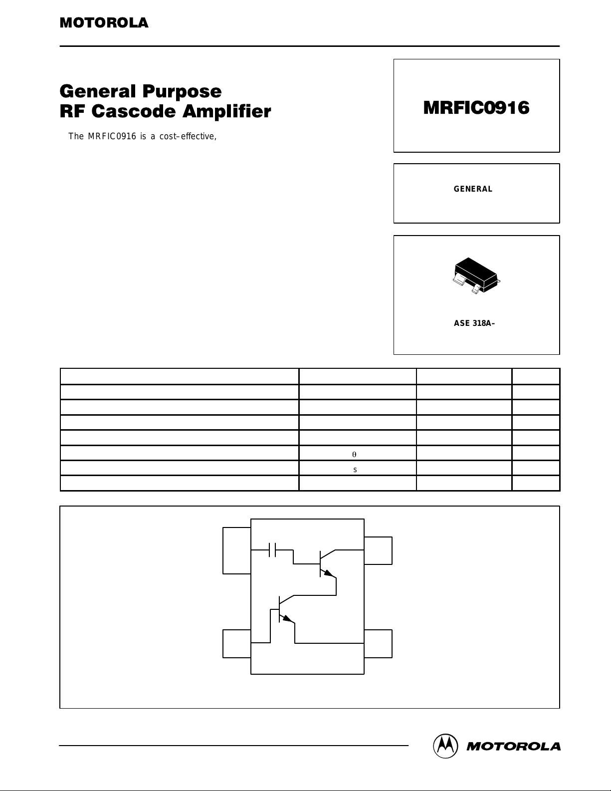
Pin Connections and Functional Block Diagram
4
GND
MRFIC0916MOTOROLA RF DEVICE DATA
1
Page 2
RECOMMENDED OPERATING RANGES
Parameter
RF Frequency f
Supply Voltage V
Symbol Value Unit
RF
CC
100 to 2500 MHz
2.7 to 5 Vdc
ELECTRICAL CHARACTERISTICS (V
Characteristic
Small Signal Gain 16.5 18.5 20.5 dB
Noise Figure — 1.9 — dB
Power Output at 1dB Gain Compression 0 2.3 — dBm
Output 3rd Order Intercept Point — 11 — dBm
Reverse Isolation — 44 — dB
Supply Current 3.8 4.7 5.6 mA
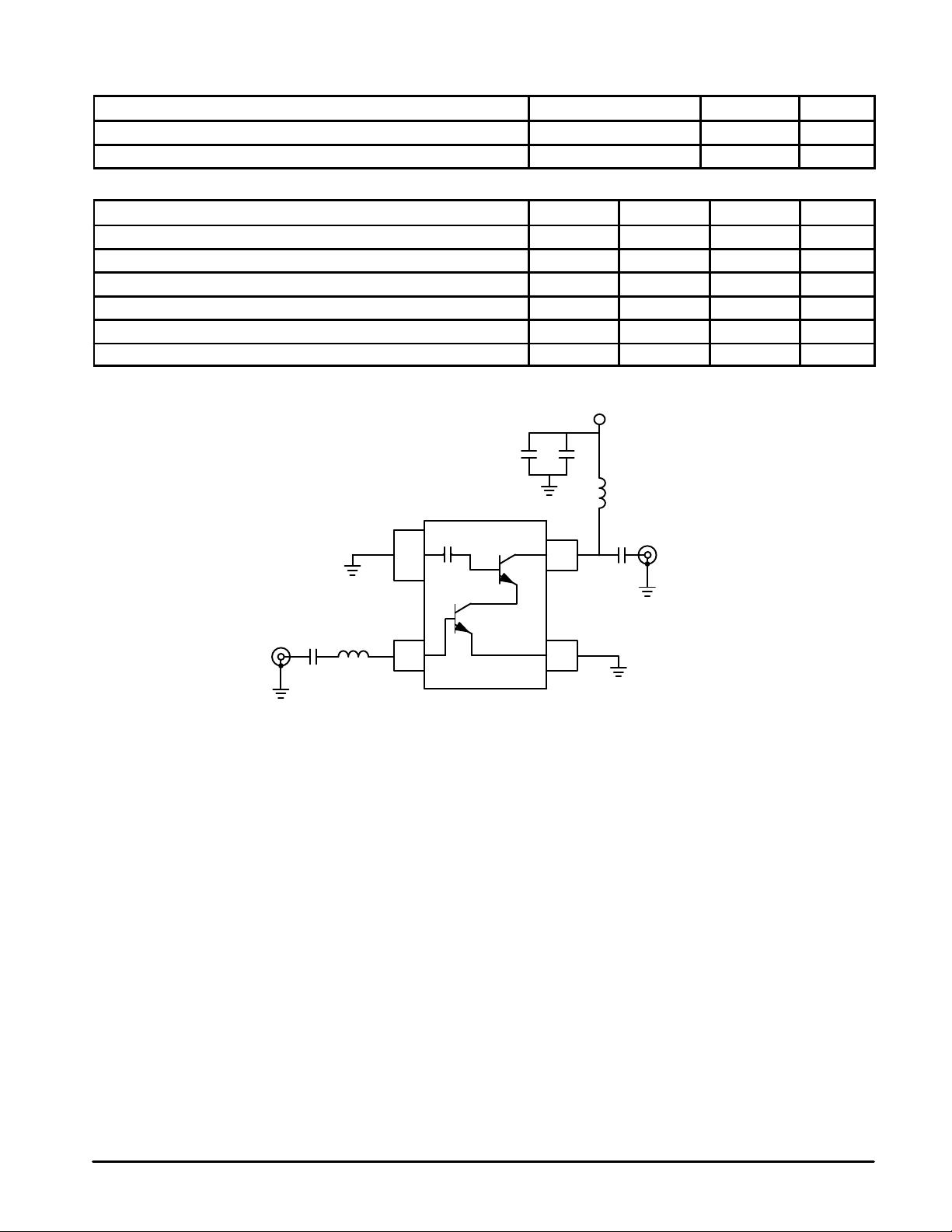
= 2.7 V, TA = 25°C, fRF = 850 MHz, Tested in Circuit Shown in Figure 1)
CC
Min Typ Max Unit
V
CC
C2
1
C1
L1
C3
3
RF OUT
RF IN
C4
L2
2
C1 – 100 pF
C2 – 0.01
C3 – 1.4 pF
C4 – 100 pF
L1 – 8.2 nH
L2 – 6.8 nH
µ
4
F
Figure 1. 850 MHz Applications Circuit Configuration
MRFIC0916
2
MOTOROLA RF DEVICE DATA
Page 3
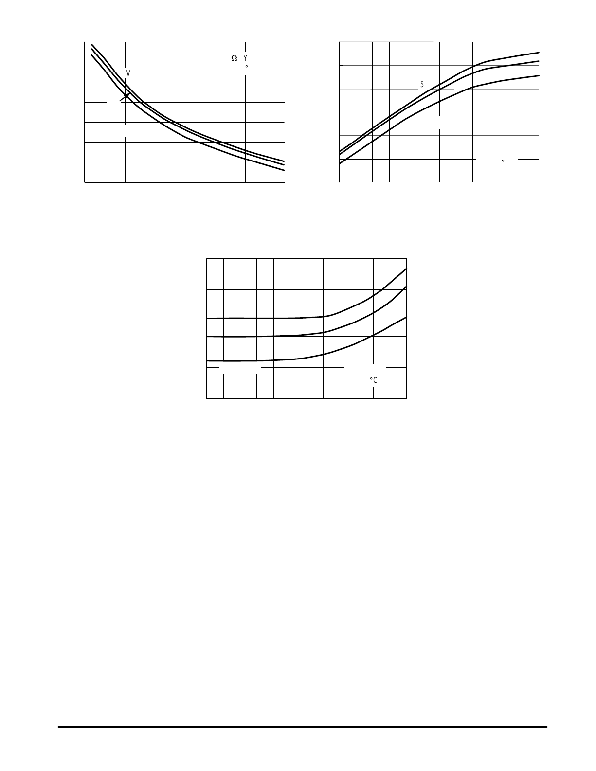
max
GU , MAXIMUM UNILATERAL GAIN (dB)
40
35
30
25
20
15
10
15
50 W SYSTEM
TA = 25
_
5 V
4 V
VCC = 2.7 V
5
0
0.5 1.0 1.5 2.0 2.5
f, FREQUENCY (GHz)
C
10
5
0
–5
, OUTPUT POWER (dBm)
out
P
–10
–15
–30
–25
5 V
VCC = 2.7 V
–20 –15 –10 –5 0
Pin, INPUT POWER (dBm)
4 V
f = 850 MHz
TA = 25
_
C
Figure 2. GU
versus Frequency
max
18
16
14
12
10
8
6
CC
4
I , SUPPLY CURRENT (mA)
2
0
–30 0–25 –20 –15 –10 –5
Figure 4. Supply Current versus Input Power
5 V
4 V
VCC = 2.7 V
f = 850 MHz
TA = 25
Pin, INPUT POWER (dBm)
Figure 3. Output Power versus Input Power
_
C
MRFIC0916MOTOROLA RF DEVICE DATA
3
Page 4

f
(MHz)
100 0.806 –17.01 12.03 162.32 0.001 –0.14 0.956 –4.69
200 0.765 –33.28 11.18 145.74 0.001 71.58 0.948 –8.69
300 0.713 –47.99 10.18 130.99 0.002 69.67 0.945 –13.23
400 0.652 –61.35 9.06 118.01 0.003 64.61 0.930 –17.35
500 0.574 –70.94 8.06 106.50 0.003 62.93 0.904 –20.85
600 0.533 –81.00 7.09 96.50 0.003 61.94 0.891 –24.71
700 0.493 –89.33 6.36 87.60 0.003 63.16 0.875 –28.18
800 0.469 –97.65 5.62 79.57 0.003 66.33 0.857 –31.89
900 0.432 –103.64 5.16 72.38 0.002 80.79 0.845 –35.21
1000 0.409 –110.68 4.70 65.39 0.002 100.33 0.831 –38.86
1100 0.396 –116.17 4.29 58.75 0.002 127.72 0.815 –42.52
1200 0.383 –122.20 3.91 52.55 0.003 152.57 0.799 –45.77
1300 0.373 –126.00 3.66 46.34 0.004 164.39 0.789 –49.49
1400 0.369 –131.29 3.38 40.61 0.006 169.63 0.776 –53.23
1500 0.366 –134.46 3.14 35.29 0.008 172.81 0.762 –56.86
1600 0.366 –140.07 2.93 29.63 0.011 172.47 0.751 –60.74
1700 0.364 –143.07 2.75 23.86 0.013 172.79 0.738 –64.66
1800 0.368 –147.48 2.58 18.42 0.016 171.54 0.727 –68.29
1900 0.377 –148.91 2.42 13.15 0.020 170.15 0.719 –72.29
2000 0.381 –153.42 2.27 7.58 0.023 167.89 0.707 –76.58
2100 0.394 –155.23 2.15 2.46 0.027 165.86 0.695 –80.50
2200 0.396 –158.91 2.03 –3.00 0.032 163.46 0.685 –84.85
2300 0.416 –160.43 1.90 –8.32 0.037 161.00 0.672 –88.93
2400 0.424 –162.98 1.81 –13.30 0.042 158.00 0.662 –93.38
2500 0.434 –166.35 1.68 –18.45 0.047 155.58 0.654 –97.89
|S11|
S
11
6 f
|S21|
S
21
6 f
|S12|
S
12
6 f
|S22|
S
22
6 f
T able 1. Scattering Parameters (VCC = 2.7 V, 50 W System)
MRFIC0916
4
MOTOROLA RF DEVICE DATA
Page 5

f
(MHz)
100 0.744 –17.43 16.979 160.38 0.001 –2.89 0.955 –4.40
200 0.691 –33.58 15.442 142.46 0.001 83.36 0.950 –8.33
300 0.627 –47.53 13.633 127.28 0.002 76.39 0.946 –12.79
400 0.558 –59.50 11.851 114.52 0.002 70.12 0.931 –16.75
500 0.482 –67.02 10.284 103.51 0.002 67.02 0.907 –20.11
600 0.440 –75.50 8.957 94.12 0.002 66.00 0.895 –23.85
700 0.401 –81.87 7.930 85.95 0.002 68.71 0.880 –27.22
800 0.377 –88.89 7.003 78.57 0.002 73.50 0.863 –30.83
900 0.348 –93.11 6.348 71.96 0.002 90.55 0.852 –34.06
1000 0.328 –98.88 5.747 65.59 0.002 113.74 0.838 –37.62
1100 0.317 –103.27 5.223 59.57 0.002 146.45 0.822 –41.18
1200 0.306 –108.54 4.765 53.98 0.003 165.49 0.808 –44.34
1300 0.301 –111.30 4.425 48.39 0.004 175.51 0.798 –47.95
1400 0.297 –116.30 4.082 43.18 0.006 177.46 0.785 –51.59
1500 0.298 –118.89 3.790 38.32 0.008 179.45 0.771 –55.11
1600 0.298 –124.58 3.531 33.13 0.011 178.69 0.760 –58.88
1700 0.301 –127.19 3.300 28.02 0.014 178.02 0.748 –62.66
1800 0.305 –131.73 3.093 23.10 0.016 176.25 0.737 –66.16
1900 0.319 –133.16 2.901 18.34 0.020 174.44 0.729 –70.03
2000 0.324 –137.94 2.724 13.33 0.023 172.03 0.717 –74.16
2100 0.339 –140.09 2.575 8.67 0.027 169.82 0.706 –77.92
2200 0.342 –143.98 2.434 3.79 0.032 166.99 0.696 –82.07
2300 0.367 –146.00 2.278 –0.98 0.036 164.37 0.684 –86.04
2400 0.375 –148.75 2.166 –5.56 0.042 161.35 0.674 –90.25
2500 0.387 –152.75 2.020 –10.12 0.046 158.69 0.666 –94.64
|S11|
S
11
6 f
|S21|
S
21
6 f
|S12|
S
12
6 f
|S22|
S
22
6 f
T able 2. Scattering Parameters (VCC = 4 V, 50 W System)
MRFIC0916MOTOROLA RF DEVICE DATA
5
Page 6

f
(MHz)
100 0.707 –17.56 20.04 159.03 0.001 –7.95 0.954 –4.25
200 0.648 –33.40 17.93 140.29 0.001 86.24 0.950 –8.15
300 0.579 –46.60 15.53 124.94 0.002 78.79 0.946 –12.54
400 0.509 –57.44 13.31 112.38 0.002 72.27 0.931 –16.42
500 0.438 –63.51 11.40 101.70 0.002 69.34 0.908 –19.68
600 0.397 –70.90 9.87 92.70 0.002 69.55 0.896 –23.35
700 0.363 –76.05 8.69 84.92 0.002 71.59 0.882 –26.64
800 0.340 –82.18 7.67 77.89 0.002 79.44 0.865 –30.20
900 0.316 –85.44 6.91 71.60 0.002 95.59 0.855 –33.36
1000 0.298 –90.52 6.24 65.56 0.001 121.55 0.841 –36.86
1100 0.290 –94.44 5.67 59.82 0.002 152.13 0.826 –40.37
1200 0.280 –99.17 5.17 54.53 0.003 169.84 0.811 –43.48
1300 0.277 –101.65 4.79 49.25 0.005 177.80 0.802 –47.02
1400 0.274 –106.49 4.42 44.27 0.006 –179.84 0.790 –50.59
1500 0.278 –109.07 4.10 39.65 0.008 –179.19 0.776 –54.04
1600 0.276 –114.88 3.82 34.68 0.011 –179.68 0.765 –57.73
1700 0.281 –117.46 3.56 29.88 0.013 179.47 0.753 –61.43
1800 0.285 –122.11 3.34 25.21 0.016 177.73 0.742 –64.85
1900 0.300 –123.94 3.14 20.70 0.019 175.80 0.734 –68.66
2000 0.305 –128.93 2.95 15.91 0.023 173.47 0.723 –72.71
2100 0.322 –131.48 2.78 11.50 0.027 171.04 0.712 –76.37
2200 0.324 –135.50 2.63 6.84 0.031 168.25 0.703 –80.42
2300 0.351 –138.04 2.47 2.33 0.036 165.47 0.691 –84.31
2400 0.358 –140.88 2.34 –2.05 0.041 162.71 0.681 –88.42
2500 0.371 –145.28 2.19 –6.40 0.046 160.19 0.674 –92.74
|S11|
S
11
6 f
|S21|
S
21
6 f
|S12|
S
12
6 f
|S22|
S
22
6 f
T able 3. Scattering Parameters (VCC = 5 V, 50 W System)
MRFIC0916
6
MOTOROLA RF DEVICE DATA
Page 7

P ACKAGE DIMENSIONS
L
34
S
1
F
H
R
A
G
2
NOTES:
1. DIMENSIONING AND TOLERANCING PER ANSI
Y14.5M, 1982.
2. CONTROLLING DIMENSION: MILLIMETER.
MILLIMETERS
DIMAMIN MAX MIN MAX
B
D
C
J
2.80 3.04 0.110 0.120
B 1.20 1.39 0.047 0.055
C 0.84 1.14 0.033 0.045
D 0.39 0.50 0.015 0.020
F 0.79 0.93 0.031 0.037
G 1.78 2.03 0.070 0.080
H 0.013 0.10 0.0005 0.004
J 0.08 0.15 0.003 0.006
K 0.46 0.60 0.018 0.024
L 0.445 0.60 0.0175 0.024
R 0.72 0.83 0.028 0.033
S 2.11 2.48 0.083 0.098
INCHES
K
CASE 318A–05
ISSUE R
MRFIC0916MOTOROLA RF DEVICE DATA
7
Page 8

Motorola reserves the right to make changes without further notice to any products herein. Motorola makes no warranty , representation or guarantee regarding
the suitability of its products for any particular purpose, nor does Motorola assume any liability arising out of the application or use of any product or circuit, and
specifically disclaims any and all liability, including without limitation consequential or incidental damages. “T ypical” parameters which may be provided in Motorola
data sheets and/or specifications can and do vary in different applications and actual performance may vary over time. All operating parameters, including “Typicals”
must be validated for each customer application by customer’s technical experts. Motorola does not convey any license under its patent rights nor the rights of
others. Motorola products are not designed, intended, or authorized for use as components in systems intended for surgical implant into the body, or other
applications intended to support or sustain life, or for any other application in which the failure of the Motorola product could create a situation where personal injury
or death may occur. Should Buyer purchase or use Motorola products for any such unintended or unauthorized application, Buyer shall indemnify and hold Motorola
and its officers, employees, subsidiaries, affiliates, and distributors harmless against all claims, costs, damages, and expenses, and reasonable attorney fees
arising out of, directly or indirectly, any claim of personal injury or death associated with such unintended or unauthorized use, even if such claim alleges that
Motorola was negligent regarding the design or manufacture of the part. Motorola and are registered trademarks of Motorola, Inc. Motorola, Inc. is an Equal
Opportunity/Affirmative Action Employer.
How to reach us:
USA/EUROPE/Locations Not Listed: Motorola Literature Distribution; JAPAN: Nippon Motorola Ltd.: SPD, Strategic Planning Office, 4–32–1,
P.O. Box 5405, Denver, Colorado 80217. 303–675–2140 or 1–800–441–2447 Nishi–Gotanda, Shinagawa–ku, Tokyo 141, Japan. 81–3–5487–8488
Mfax: RMFAX0@email.sps.mot.com – TOUCHTONE 602–244–6609 ASIA/PACIFIC: Motorola Semiconductors H.K. Ltd.; 8B Tai Ping Industrial Park,
– US & Canada ONLY 1–800–774–1848 51 Ting Kok Road, T ai Po, N.T., Hong Kong. 852–26629298
INTERNET: http://motorola.com/sps
Mfax is a trademark of Motorola, Inc.
MRFIC0916
8
◊
MOTOROLA RF DEVICE DATA
MRFIC0916/D
 Loading...