

Page 1
SEMICONDUCTOR TECHNICAL DATA
The MRFIC Line
Order this document
by MRFIC0914/D
!
This integrated circuit is intended for two–way paging applications and for
other Industrial, Scientific and Medical (ISM) at 900 MHz band applications.
The three stage design is implemented in Motorola’s low cost, high performance LDMOS process and housed in a low–cost surface mount SOIC
package. Input and output matching is implemented off–chip for maximum
flexibility while interstage matching is on–chip. A power control pin is included
allowing 60 dB dynamic range.
• 30.5 dBm Output Power for 3 dBm Input Power at 900 MHz
• 32 dB Typ Small Signal Gain
• 40% Efficiency Min at 30.5 dBm Output Power
• 4.0 to 5.5 Volt Operation
• Low–Cost, Low Profile Plastic SOIC Package
• Order MRFIC0914R2 for Tape and Reel.
R2 Suffix = 2,500 Units per 16 mm, 13 inch Reel.
• Device Marking = M0914
ABSOLUTE MAXIMUM RATINGS
Supply Voltage V
Supply Current I
Power Control Voltage V
Input Power P
Ambient Operating Temperature T
Storage Temperature T
Thermal Resistance, Junction to Case θ
(TA = 25°C unless otherwise noted)
Rating
Symbol Value Unit
D1, VD2, VD3
Dtotal
CNTRL
stg
JC
900 MHz PAGING
POWER AMPLIFIER
Si MONOLITHIC
INTEGRATED CIRCUIT
CASE 751B–05
(SOIC–16)
9 Vdc
2 Adc
4.8 Vdc
in
A
6 dBm
–30 to +80 °C
–65 to +150 °C
26 °C/W
REV 2
Motorola, Inc. 1997
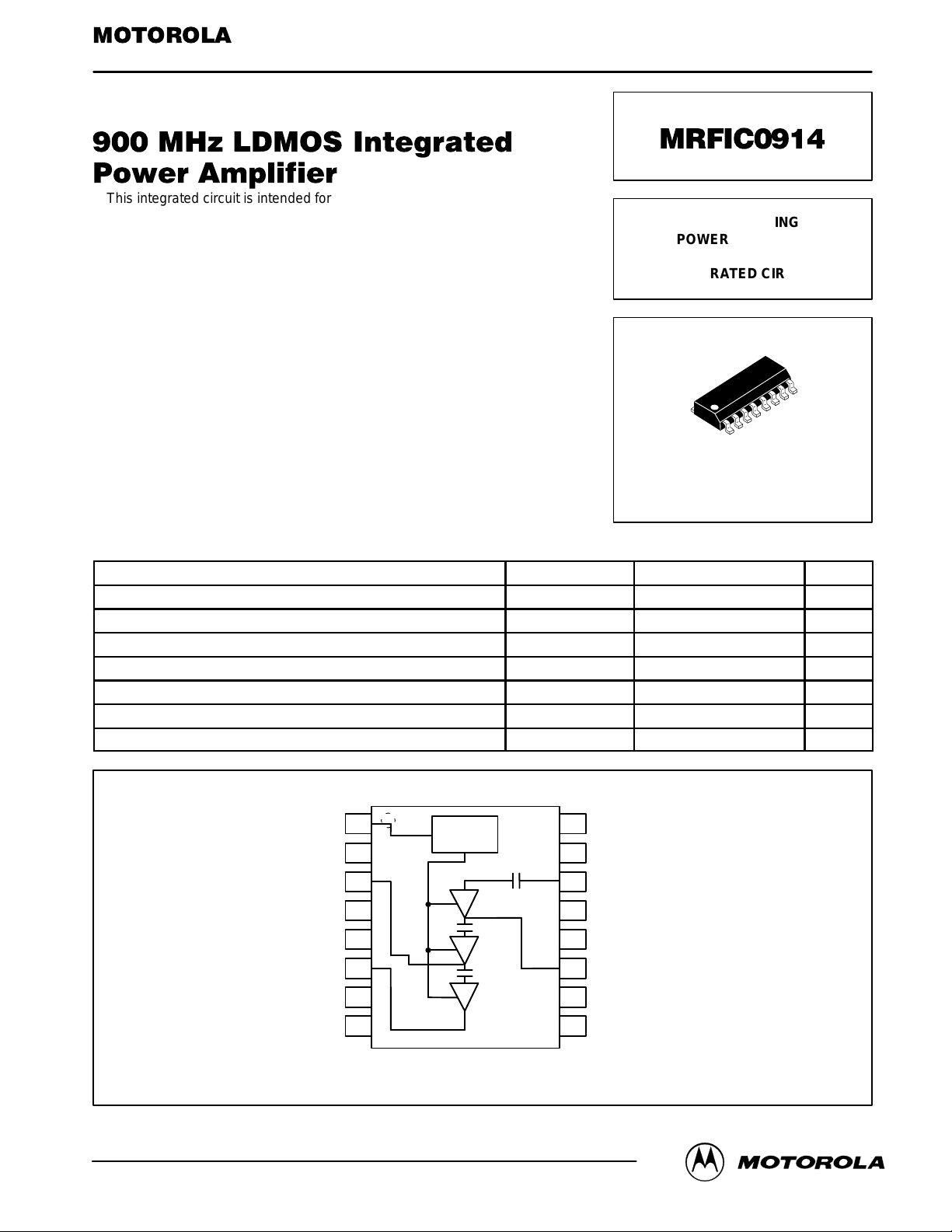
V
CNTRL
GND
V
GND
GND
RF OUT/V
GND
GND
D2
D3
1
2
3
4
5
6
7
8
CONTROL
16
15
14
13
12
11
10
GND
GND
RF IN
GND
GND
V
D1
GND
9
GND
Pin Connections and Functional Block Diagram
MRFIC0914MOTOROLA RF DEVICE DATA
1
Page 2
RECOMMENDED OPERATING RANGES
Parameter Symbol Value Unit
Supply Voltage VD1, VD2,
Power Control Voltage V
RF Frequency Range f
V
CNTRL
RF
3.6 to 5.8 Vdc
D3
0 to 4.8 Vdc
890 to 928 MHz
ELECTRICAL CHARACTERISTICS (V
I
= 583 mA, TA = 25°C unless otherwise noted. Measured in Circuit Configuration Shown in Figure 1.)
Dtotal
Characteristic
Output Power 1.12 — — W
Efficiency 40 — — %
Output Power at 1 dB Gain Compression — 29 — dBm
Saturated Output Power — 31 — dBm
Output Third Order Intercept Point — 36 — dBm
Dynamic Range (V
Input Return Loss 7 12 — dB
Output Power, Low Voltage (VD1, VD2, VD3 = 3.84 V) 0.56 — — W
Spurious Output (Load VSWR = 20:1, All Phase Angles) — –60 –50 dBc
Harmonic Output (With External Matching Circuit) — — –45 dBc
RF OUT
= 0 to 4.8 V) — 60 — dB
CNTRL
V
CNTRL
V
D2
V
D3
C1
C10
C9
C2
, VD2, VD3 = 4.8 V, f = 900 MHz, Pin = 3 dBm, 1 ms, 10% duty cycle, V
D1
Min Typ Max Unit
C8
C4
1
2
3
C5
4
L
1
T1T2
C3
5
6
7
CONTROL
16
15
14
13
12
11
10
C6
L2
C7
CNTRL
RF INPUT
V
D3
Adjusted for
MRFIC0914
2
L
3
µ
C1, C7 — 0.01
C2, C6, C8 — 33 pF
C3 — 12 pF
C4 — 1.0
f
µ
F
8
C5, C10 — 100 pF
C9 — 2.1 pF
L1 — 33 nH
L2 — 5.6 nH
L3 — 3.3 nH
Ω
T1 — 50
T2 — 50
BOARD MATERIAL — 18 MIL FR4
MICROSTRIP, 7.5° @ 900 MHz
Ω
MICROSTRIP, 31.6° @ 900 MHz
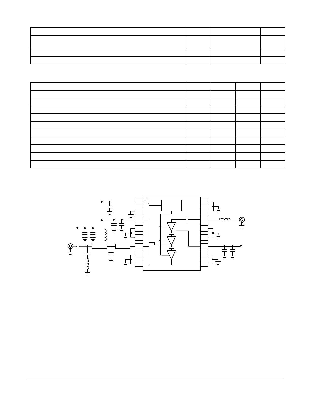
Figure 1. Application Circuit Configuration
9
MOTOROLA RF DEVICE DATA
Page 3

3
4
3
2
3
0
2
8
2
6
2
out
P , OUTPUT POWER (dBm)
4
2
2
2
–10 –7.5 –5 –2.5 0 2.5 5
0
Pin, INPUT POWER (dBm)
5.8 V
4.8 V
V
D1, VD2, VD3
TA = 25°C
f = 900 MHz
V
CNTRL
Figure 2. Output Power versus Input Power Figure 3. Output Power versus Input Power
= 3.6 V
= 4 V
3
2
3
0
2
8
2
6
2
4
2
out
P , OUTPUT POWER (dBm)
2
2
0
1
–10 –7.5 –5 –2.5 0 2.5 5
8
–35°C
°
C
25
TA = 85°C
f = 900 MHz
V
CNTRL
V
D1, VD2, VD3
Pin, INPUT POWER (dBm)
= 4 V
= 4.8 V
700
TA = 25°C
f = 900 MHz
650
V
= 4 V
CNTRL
600
550
500
TOTAL SUPPL Y CURRENT (mA)
450
–10 –7.5 –5 –2.5 0 2.5 5
Pin, INPUT POWER (dBm)
5.8 V
4.8 V
V
D1, VD2, VD3
= 3.6 V
Figure 4. Supply Current versus Input Power Figure 5. Supply Current versus Input Power
4
0
3
0
2
0
1
0
0
V
–10
–20
out
P , OUTPUT POWER (dBm)
–30
–40
012345
V
CNTRL
D1, VD2, VD3
5.8 V
, CONTROL VOLTAGE (VOLTS)
5.8 V
4.8 V
= 3.6 V
TA = 25°C
f = 900 MHz
Pin = 3 dBm
700
650
600
550
500
TOTAL SUPPL Y CURRENT (mA)
450
400
–10 –7.5 –5 –2.5 0 2.5 5
900
800
V
D1, VD2, VD3
700
600
500
400
300
200
TOTAL QUIESCENT CURRENT (mA)
100
0
01 2 34 5
V
–35°C
°
25
C
TA = 85°C
Pin, INPUT POWER (dBm)
= 3.6 to 5.8 V
, CONTROL VOLTAGE (VOLTS)
CNTRL
f = 900 MHz
V
= 4 V
CNTRL
V
D1, VD2, VD3
25°C
–35°C
TA = 85°C
= 4.8 V
Figure 6. Output Power versus V
CNTRL
Figure 7. Quiescent Current versus V
MRFIC0914MOTOROLA RF DEVICE DATA
CNTRL
3
Page 4

30.75
620
30.50
TA = 25°C
30.25
f = 900 MHz
V
= 4 V, 5 ms PULSE
out
P , OUTPUT POWER (dBm)
30.00
CNTRL
V
D1, VD2, VD3
Pin = 3 dBm
0 20 40 60 80 100
= 4.8 V
DUTY CYCLE (%)
I
Dtotal
P
out
600
580
TOTAL SUPPL Y CURRENT (mA)
560
Figure 8. Output Power versus Duty Cycle
f Zin (Ω) Z
MHz R jX R jX
800 48.8 –16.3 2.56 14.3
850 49.0 –17.9 3.30 14.4
900 49.0 –19.6 2.80 13.1
950 49.4 –21.2 3.94 14.0
1000 49.8 –23.1 3.95 12.6
OL
*
(Ω)
T able 1. Device Impedances Derived from Circuit Characterization
APPLICATIONS INFORMATION
DESIGN PHILOSOPHY
The MRFIC0914 three stage LDMOS integrated power
amplifier was designed for low cost and flexibility. While the
target application was two–way paging, the device can be
used in a variety of 800 to 1000 MHz applications and it is
particularly suited to burst mode digital transmissions with
constant envelope modulation schemes. Only one supply is
required. The V
CNTRL
of the three stages simultaneoulsy for optimum gain and efficiency and serves as a transmit control with more than 60 dB
dynamic range.
CIRCUIT DETAILS
In Figure 1, the 900 MHz applications circuit, note that
each stage has a separate supply pin, including the RF Output for the third stage. Care should be taken in bypassing
these supply connections to avoid low frequency oscillation.
Chip capacitors should be mounted as close to the leads and
ground vias as possible. Ground vias should be provided
close to the indicated ground leads as well. L1 is a bias
choke supplying the third stage and could be replaced with a
quarter wave line or air–wound inductor.
pin allows the setting of the gate bias
RF performance is sensitive to the output matching network. C9 and L3 form a second harmonic trap which enhances efficiency. Placement of C3 along the 50Ω line at the
device output is critical to gain and efficiency. L2, the input
matching inductor, is optional. Without this inductor, the input
match is still typically better than 2:1 VSWR.
It should be note that Figure 1 does not portray the parasitics of the chip components nor their solder mounting pads.
The board material is 18 mil dielectric thickness FR4. The impedances shown in Table 1 were derived from circuit characterization and are given as an aid to original designs.
EVALUATION BOARDS
Evaluation boards are available for RF Monolithic Integrated Circuits by adding a “TF” to the device type. For a
complete list of currently available boards and ones in development for newly introduced products, please consult your
local Motorola Distributor or Sales Office.
MRFIC0914
4
MOTOROLA RF DEVICE DATA
Page 5

P ACKAGE DIMENSIONS
-T-
SEATING
PLANE
-A-
NOTES:
1. DIMENSIONING AND TOLERANCING PER ANSI
916
-B-
P 8 PL
1
8
0.25 (0.010) B
M M
G
K
R X 45°
F
C
J
D
16 PL
0.25 (0.010) T B A
M
M
S S
Y14.5M, 1982.
2. CONTROLLING DIMENSION: MILLIMETER.
3. DIMENSIONS A AND B DO NOT INCLUDE
MOLD PROTRUSION.
4. MAXIMUM MOLD PROTRUSION 0.15 (0.006)
PER SIDE.
5. DIMENSION D DOES NOT INCLUDE DAMBAR
PROTRUSION. ALLOWABLE DAMBAR
PROTRUSION SHALL BE 0.127 (0.005) TOTAL
IN EXCESS OF THE D DIMENSION AT
MAXIMUM MATERIAL CONDITION.
MILLIMETERS INCHES
MIN MINMAX MAX
DIM
A
9.80
B
3.80
C
1.35
D
0.35
F
0.40
1.27 BSC 0.050 BSC
G
J
0.19
K
0.10
M
0
°
P
5.80
R
0.25
10.00
4.00
1.75
0.49
1.25
0.25
0.25
7
6.20
0.50
°
0.386
0.150
0.054
0.014
0.016
0.008
0.004
0
°
0.229
0.010
0.393
0.157
0.068
0.019
0.049
0.009
0.009
7
°
0.244
0.019
CASE 751B-05
ISSUE J
MRFIC0914MOTOROLA RF DEVICE DATA
5
Page 6

Motorola reserves the right to make changes without further notice to any products herein. Motorola makes no warranty , representation or guarantee regarding
the suitability of its products for any particular purpose, nor does Motorola assume any liability arising out of the application or use of any product or circuit, and
specifically disclaims any and all liability, including without limitation consequential or incidental damages. “T ypical” parameters which may be provided in Motorola
data sheets and/or specifications can and do vary in different applications and actual performance may vary over time. All operating parameters, including “Typicals”
must be validated for each customer application by customer’s technical experts. Motorola does not convey any license under its patent rights nor the rights of
others. Motorola products are not designed, intended, or authorized for use as components in systems intended for surgical implant into the body, or other
applications intended to support or sustain life, or for any other application in which the failure of the Motorola product could create a situation where personal injury
or death may occur. Should Buyer purchase or use Motorola products for any such unintended or unauthorized application, Buyer shall indemnify and hold Motorola
and its officers, employees, subsidiaries, affiliates, and distributors harmless against all claims, costs, damages, and expenses, and reasonable attorney fees
arising out of, directly or indirectly, any claim of personal injury or death associated with such unintended or unauthorized use, even if such claim alleges that
Motorola was negligent regarding the design or manufacture of the part. Motorola and are registered trademarks of Motorola, Inc. Motorola, Inc. is an Equal
Opportunity/Affirmative Action Employer.
How to reach us:
USA/EUROPE/Locations Not Listed: Motorola Literature Distribution; JAPAN: Nippon Motorola Ltd.: SPD, Strategic Planning Office, 4–32–1,
P.O. Box 5405, Denver, Colorado 80217. 303–675–2140 or 1–800–441–2447 Nishi–Gotanda, Shinagawa–ku, Tokyo 141, Japan. 81–3–5487–8488
Mfax: RMFAX0@email.sps.mot.com – TOUCHTONE 602–244–6609 ASIA/PACIFIC: Motorola Semiconductors H.K. Ltd.; 8B Tai Ping Industrial Park,
– US & Canada ONLY 1–800–774–1848 51 Ting Kok Road, T ai Po, N.T., Hong Kong. 852–26629298
INTERNET: http://motorola.com/sps
Mfax is a trademark of Motorola, Inc.
MRFIC0914
6
◊
MOTOROLA RF DEVICE DATA
MRFIC0914/D
 Loading...