

Page 1
SEMICONDUCTOR TECHNICAL DATA
The MRFIC Line
!
Designed primarily for use in high efficiency Analog Cellular applications,
the MRFIC0912 is a two–stage power amplifier in Motorola’s proprietary
Power Flat Pack 16–lead package. This integrated circuit requires minimal
off-chip matching while allowing for the maximum in flexibility in optimizing
gain and efficiency. The design employs Motorola’s planar, self–aligned GaAs
MESFET IC process to give the highest efficiency possible.
• Usable Frequency Range = 800–1000 MHz, Specified for 824–905 MHz
• 30.8 dBm Minimum Output Power
• 470 mA Maximum Supply Current at 30.8 dBm Output
• 23.8 dB Minimum Gain
• Simple Off–chip Matching for Maximum Power/Efficiency Flexibility
• 4.6 Volt Supply
• 45 dB/Volt Typical Power Output Control
• Order MRFIC0912R2 for Tape and Reel Option.
R2 Suffix = 1,500 Units per 16 mm, 13 inch Reel.
• Device Marking = M0912
Order this document
by MRFIC0912/D
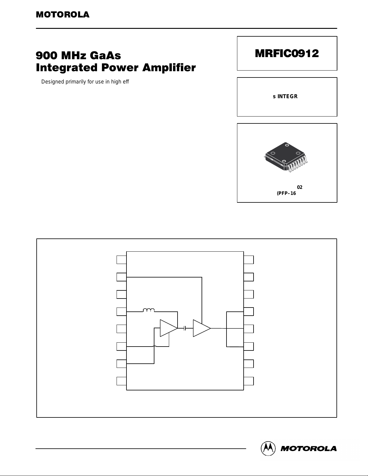
900 MHz
GaAs INTEGRATED
POWER AMPLIFIER
CASE 978–02
(PFP–16)
GND
V
N/C
V
D1
N/C
V
G1
RF IN
N/C
G2
1
2
3
4
5
6
7
8
Pin Connections and Functional Block Diagram
16
15
14
13
12
11
10
9
N/C
N/C
N/C
RF OUT/V
RF OUT/V
RF OUT/V
N/C
GND
D2
D2
D2
REV 1
Motorola, Inc. 1997
MOTOROLA RF DEVICE DATA
MRFIC0912
1
Page 2
MAXIMUM RATINGS
(TA = 25°C unless otherwise noted)
Ratings Symbol Limit Unit
Supply Voltage VD1, V
RF Input Power P
Gate Voltage VG1, VG2, V
Storage Temperature Range T
Operating Case Temperature T
Thermal Resistance, Junction to Case R
RF
stg
C
θJC
RECOMMENDED OPERATING RANGES
Parameter
RF Frequency f
Supply Voltage VD1, V
Gate Voltage VG1, V
Symbol Value Unit
RF
D2
D2
G2
GG
8 Vdc
20 dBm
–5 Vdc
– 65 to +150 °C
– 35 to +100 °C
18 °C/W
824–905 MHz
4.0–6.0 Vdc
–2.3 to –1.5 Vdc
ELECTRICAL CHARACTERISTICS (V
Circuit Shown in Figure 1)
Characteristic
RF Output Power 30.8 31.2 — dBm
Power Slump (VD1, VD2 = 4.0 V, TC = 100_C)
Load Mismatch Survival (VD1, VD2 = 7 V, Load VSWR = 10:1, all phases,
10 sec)
Spurious Output (VD1,VD2 = 0 to 7 V, Pin = 5 to 9 dBm, Load
VSWR = 10:1)
Input Return Loss — 10 — dB
Harmonic Output (P
2f
0
3f
0
4f
0
Noise Power (VDD = 0 to 7 V, 45 MHz Above fRF at 30 kHz BW) — — –93 dBm
Maximum Power Control Voltage Slope (Change in P
VD1)
Total Supply Current (VD1 set for P
VGG Required for I
Gate Current during RF Operation –2 — 2 mA
= 30.8 dBm)
out
out
= 200 mA –2.3 –2.0 –1.7 Vdc
D2Q
, VD2 = 4.6 V , TA = 25°C, fRF = 840 MHz, Pin = 7 dBm, VGG set for I
D1
Min Typ Max Unit
28.5 — — dBm
No Degradation
— — –60 dBc
—
—
—
for Change on
out
= 30.8 dBm) — 430 470 mA
— 45 — dB/V
—
—
—
= 200 mA, T ested in
D2Q
–25
–40
–40
dBc
DESIGN AND APPLICATIONS INFORMATION
The MRFIC0912 has been designed for high efficiency
900 MHz applications such as analog cellular and Industrial,
Medical and Scientific (ISM) equipment. The two stage MESFET design utilizes Motorola’s planar refractory gate process
to allow high performance GaAs to be applied to consumer
applications. The proprietary PFP–16 package assures good
grounding and low thermal resistance.
As shown in Figure 1, the gate voltage pins can be ganged
together and one voltage applied to both gates to set the
quiescent operating current. Alternatively , VG1 and VG2 can
be set separately. VD1 can be used as power control with a
45 dB per volt sensitivity. The placement of C3 in the V
D1
supply line can be varied to optimize RF performance since
T2 is part of a shunt L matching section. On the output, pins
MRFIC0912
2
11, 12 and 13, the placement of C11 is adjusted for best RF
performance.
Layout is important for amplifier stability and RF performance. Ground vias must be located as close to circuit
ground connections as possible. Power supply bypassing
C3, C6, C9, and C10 must be included to reduce out–of–
band gain and prevent spurious output.
Evaluation Boards
Evaluation boards are available for RF Monolithic Integrated Circuits by adding a “TF” suffix to the device type.
For a complete list of currently available boards and ones
in development for newly introduced product, please con tact your local Motorola Distributor or Sales Office.
MOTOROLA RF DEVICE DATA
Page 3

C5
1
2
V
G2
3
4
V
GG
C3
T2
C6
V
D1
16
15
14
13
L2
C9
C10
V
D2
35
30
25
RF IN
VDD = 4.6 V
R1
C4
L1
C2
C1
R1 1 kΩ
C1 3.3 pF
C2, C3, C8, C9 100 pF
C11 8.2 pF
Figure 1. Applications Circuit Configuration
5
6
V
G1
7
8
C6 0.01 µF
C10 1 µF
C4, C5 1000 pF
L1 10 nH
TYPICAL CHARACTERISTICS
VDD = 5.8 V
VDD = 4.0 V
35
30
25
12
T1
11
10
9
L2 22 nH
T1 50 Ω, 13° @ 840 MHz
T2 50 Ω, 8° @ 840 MHz
BOARD MATERIAL — GLASS/EPOXY, εr =
4.45, THICKNESS = 18 MIL
85°C
C11
RF OUT
C8
T = 25°C
, OUTPUT POWER (dBm)
20
out
P
15
Pin, INPUT POWER (dBm)
Figure 2. Output Power versus Input Power
MOTOROLA RF DEVICE DATA
, OUTPUT POWER (dBm)
20
out
f = 837 MHz
TEMP = 25
0–5
°
C
5
10
P
15
–10 10–10 05
–35°C
VDD = 4.6 V
f = 837 MHz
–5
Pin, INPUT POWER (dBm)
Figure 3. Output Power versus Input Power
MRFIC0912
3
Page 4

TYPICAL CHARACTERISTICS
35
VDD = 5.8 V
25
15
, OUTPUT POWER (dBm)
5
out
P
–5
0
13
V
VDD = 4.0 V
f = 837 MHz
Pin = 7.0 dBm
TEMP = 25
246
, CONTROL VOLTAGE (VOLTS)
cntrl
Figure 4. Output Power versus Control Voltage
70
60
50
40
VDD = 4.0 V
VDD = 4.6 V
°
C
5
35
85°C
25
15
, OUTPUT POWER (dBm)
5
out
P
–5
120
V
cntrl
T = 25°C
–35°C
VDD = 4.6 V
f = 837 MHz
Pin = 7.0 dBm
345
, CONTROL VOLTAGE (VOLTS)
Figure 5. Output Power versus Control Voltage
70
60
50
40
T = 25°C
85°C
PAE, POWER ADDED EFFICIENCY (%)
PAE, POWER ADDED EFFICIENCY (%)
30
20
10
0
–10
–5 10
VDD = 4.6 V
VDD = 5.8 V
0
Pin, INPUT POWER (dBm)
Figure 6. Power Added Efficiency versus
Input Power
70
60
VDD = 4.0 V
50
40
30
20
10
0
V
, CONTROL VOLTAGE (VOLTS)
cntrl
VDD = 4.6 V
VDD = 5.8 V
4321
Figure 8. Power Added Efficiency versus
Control Voltage
f = 837 MHz
TEMP = 25
5
f = 837 MHz
Pin = 7.0 dBm
TEMP = 25
°
°
C
5
30
20
10
C
PAE, POWER ADDED EFFICIENCY (%)
0
–5
Pin, INPUT POWER (dBm)
0
–35°C
VDD = 4.6 V
f = 837 MHz
5
10–10
Figure 7. Power Added Efficiency versus
Input Power
70
60
50
40
30
20
10
PAE, POWER ADDED EFFICIENCY (%)
6
0
050
1
V
cntrl
T = 25°C
–35°C
VDD = 4.6 V
f = 837 MHz
Pin = 7.0 dBm
23
, CONTROL VOLTAGE (VOLTS)
85°C
4
Figure 9. Power Added Efficiency versus
Control Voltage
MRFIC0912
4
MOTOROLA RF DEVICE DATA
Page 5

TYPICAL CHARACTERISTICS
34
VDD = 5.8 V
33
32
VDD = 4.6 V
31
, OUTPUT POWER (dBm)
VDD = 4.0 V
out
P
30
29
825
835830 840
f, FREQUENCY (MHz)
Figure 10. Output Power versus Frequency
62
VDD = 4.6 V
61
Pin = 7.0 dBm
TEMP = 25
845
°
C
850
31.8
31.6
31.4
31.2
31
, OUTPUT POWER (dBm)
30.8
out
P
30.6
30.4
VDD = 4.6 V
Pin = 7.0 dBm
Figure 11. Output Power versus Frequency
63
61
–35°C
T = 25°C
85°C
830 835825
f, FREQUENCY (MHz)
T = 25°C
840 845 850
–35°C
60
PAE, POWER ADDED EFFICIENCY (%)
59
VDD = 4.0 V
VDD = 5.8 V
825
830 850
f, FREQUENCY (MHz)
Figure 12. Power Added Efficiency
versus Frequency
840
, DRAIN CURRENT (mA)
D2
I
D1
I ,
59
57
Pin = 7.0 dBm
TEMP = 25
450
400
350
300
250
200
150
100
50
0
0
°
C
845835
V
, CONTROL VOLTAGE (VOLTS)
cntrl
I
I
D1
PAE, POWER ADDED EFFICIENCY (%)
55
D2
Figure 14. Drain Current versus Control
V oltage
85°C
VDD = 4.6 V
Pin = 7.0 dBm
830
835 845
f, FREQUENCY (MHz)
840
Figure 13. Power Added Efficiency
versus Frequency
VDD = 4.6 V
f = 837 MHz
Pin = 7.0 dBm
321
4
5
850825
MOTOROLA RF DEVICE DATA
MRFIC0912
5
Page 6

P ACKAGE DIMENSIONS
X 45
h
_
A
E2
e
14 x
A
e/2
A2
1
8
E1
8X E
M
bbb C
DETAIL Y
ccc C
16
D
9
B
S
B
DATUM
H
PLANE
BOTTOM VIEW
b1
c
c1
b
S
A
C
SEATING
PLANE
M
aaa C
SECT W–W
L1
q
W
W
L
1.000
0.039
DETAIL Y
GAUGE
PLANE
A1
CASE 978–02
ISSUE A
D1
NOTES:
1. CONTROLLING DIMENSION: MILLIMETER.
2. DIMENSIONS AND TOLERANCES PER ASME
Y14.5M, 1994.
3. DATUM PLANE –H– IS LOCATED AT BOTTOM OF
LEAD AND IS COINCIDENT WITH THE LEAD
WHERE THE LEAD EXITS THE PLASTIC BODY AT
THE BOTTOM OF THE PARTING LINE.
4. DIMENSIONS D AND E1 DO NOT INCLUDE MOLD
PROTRUSION. ALLOWABLE PROTRUSION IS
0.250 PER SIDE. DIMENSIONS D AND E1 DO
INCLUDE MOLD MISMATCH AND ARE
DETERMINED AT DATUM PLANE –H–.
5. DIMENSION b DOES NOT INCLUDE DAMBAR
PROTRUSION. ALLOWABLE DAMBAR
PROTRUSION IS 0.127 TOTAL IN EXCESS OF THE
b DIMENSION AT MAXIMUM MATERIAL
CONDITION.
6. DATUMS –A– AND –B– TO BE DETERMINED AT
DATUM PLANE –H–.
MILLIMETERS
DIM MIN MAX
A 2.000 2.350
A1 0.025 0.152
A2 1.950 2.100
D 6.950 7.100
D1 4.372 5.180
E 8.850 9.150
E1 6.950 7.100
E2 4.372 5.180
L 0.466 0.720
L1 0.250 BSC
b 0.300 0.432
b1 0.300 0.375
c 0.180 0.279
c1 0.180 0.230
e 0.800 BSC
h ––– 0.600
q
0 7
__
aaa 0.200
bbb 0.200
ccc 0.100
Motorola reserves the right to make changes without further notice to any products herein. Motorola makes no warranty , representation or guarantee regarding
the suitability of its products for any particular purpose, nor does Motorola assume any liability arising out of the application or use of any product or circuit, and
specifically disclaims any and all liability, including without limitation consequential or incidental damages. “T ypical” parameters which may be provided in Motorola
data sheets and/or specifications can and do vary in different applications and actual performance may vary over time. All operating parameters, including “Typicals”
must be validated for each customer application by customer’s technical experts. Motorola does not convey any license under its patent rights nor the rights of
others. Motorola products are not designed, intended, or authorized for use as components in systems intended for surgical implant into the body, or other
applications intended to support or sustain life, or for any other application in which the failure of the Motorola product could create a situation where personal injury
or death may occur. Should Buyer purchase or use Motorola products for any such unintended or unauthorized application, Buyer shall indemnify and hold Motorola
and its officers, employees, subsidiaries, affiliates, and distributors harmless against all claims, costs, damages, and expenses, and reasonable attorney fees
arising out of, directly or indirectly, any claim of personal injury or death associated with such unintended or unauthorized use, even if such claim alleges that
Motorola was negligent regarding the design or manufacture of the part. Motorola and are registered trademarks of Motorola, Inc. Motorola, Inc. is an Equal
Opportunity/Affirmative Action Employer.
Mfax is a trademark of Motorola, Inc.
How to reach us:
USA/EUROPE/Locations Not Listed: Motorola Literature Distribution; JAPAN: Nippon Motorola Ltd.; Tatsumi–SPD–JLDC, 6F Seibu–Butsuryu–Center,
P.O. Box 5405, Denver, Colorado 80217. 303–675–2140 or 1–800–441–2447 3–14–2 Tatsumi Koto–Ku, Tokyo 135, Japan. 81–3–3521–8315
Mfax: RMFAX0@email.sps.mot.com – TOUCHTONE 602–244–6609 ASIA/PACIFIC: Motorola Semiconductors H.K. Ltd.; 8B Tai Ping Industrial Park,
– US & Canada ONLY 1–800–774–1848 51 Ting Kok Road, T ai Po, N.T., Hong Kong. 852–26629298
INTERNET: http://motorola.com/sps
MRFIC0912
◊
MOTOROLA RF DEVICE DATA
MRFIC0912/D
6
 Loading...