

Page 1
SEMICONDUCTOR TECHNICAL DATA
The MRFIC Line
! ""
The MRFIC0904 is an integrated driver amplifier designed for class A/B
operation in the 800 MHz to 1 GHz frequency range. The design utilizes
Motorola’s Advanced GaAs FET process to yield superior performance and
efficiency in a cost effective monolithic device. Off–chip output matching provides maximum flexibility in design. Applications for the MRFIC0904 include
GSM, AMPS, and ISM band transmitters.
• GSM Ramping/Gain Control of 45 dB with Power Control Function (PCNTRL)
• Class 4 P
• Class 4 Supply Current (1 dB) = 120 mA @ 4.8 V (Typical)
• Class 5 P
• Class 5 Supply Current (1 dB) = 120 mA @ 3.6 V (Typical)
• Low Cost Surface Mount Plastic Package
• Order MRFIC0904R2 for Tape and Reel.
R2 Suffix = 2,500 Units per 16 mm, 13 inch Reel.
• Device Marking = M0904
(1 dB Gain Compression) = 26 dBm @ 4.8 V (Typical)
out
(1 dB Gain Compression) = 24 dBm 3.6 V (Typical)
out
Order this document
by MRFIC0904/D
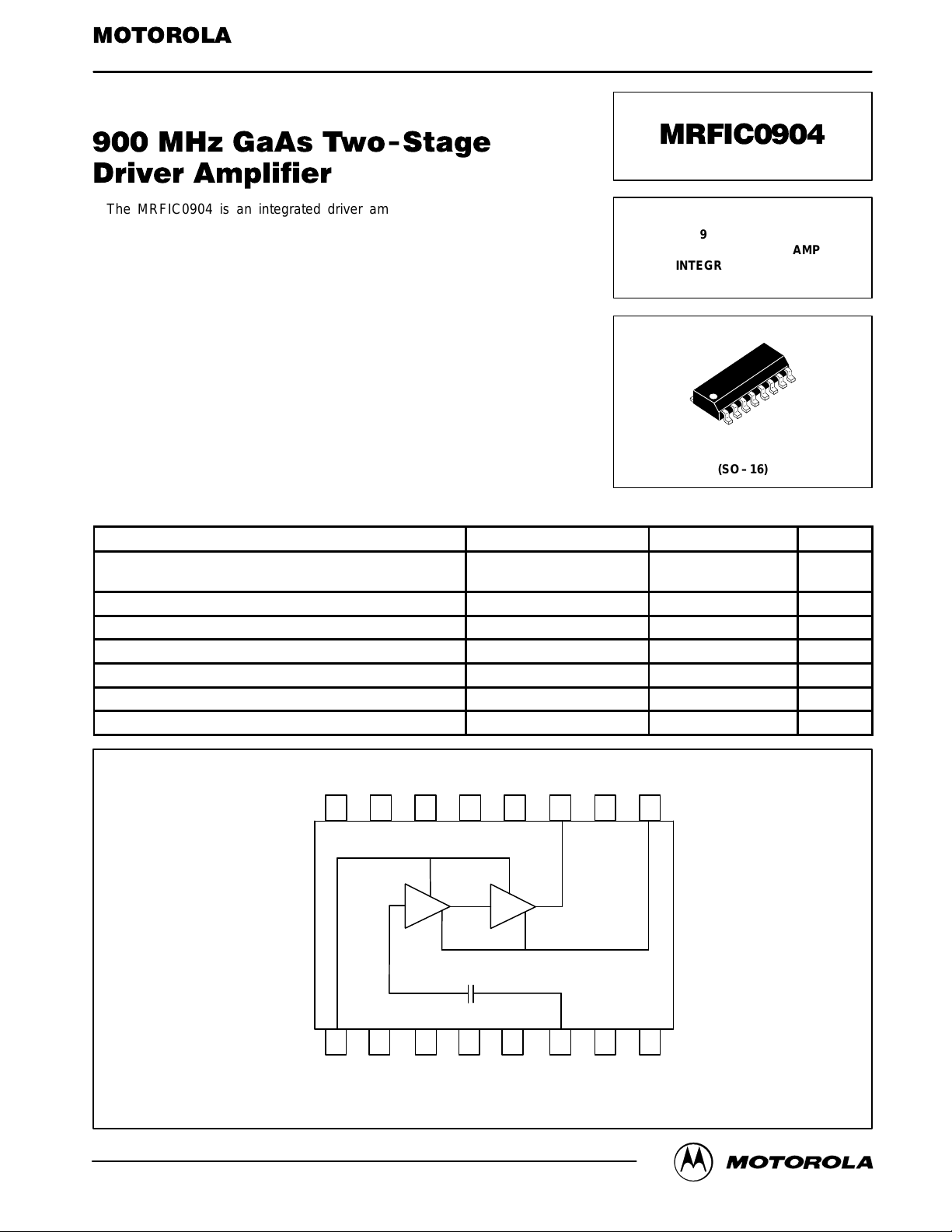
900 MHz GaAs
TWO STAGE DRIVER AMP
INTEGRATED CIRCUIT
CASE 751B–05
(SO–16)
MAXIMUM RATINGS
(TA = 25°C unless otherwise noted)
Rating Symbol Limit Unit
Supply Voltage V
Power Control Voltage PCNTRL V
Enable Voltage ENABLE V
Input Power P
Operating Ambient Temperature T
Storage Temperature T
Thermal Resistance, Junction to Case θ
ENABLE
16
GND
DD
GNDGND
DD
V
SS
in
A
stg
JC
RF OUT
1112131415
10
– 35 to +85 °C
–65 to +150 °C
BIASGNDV
9
6.0
–3
DD
DD
5 dBm
60 °C/W
Vdc
Vdc
Vdc
REV 2
Motorola, Inc. 1997
1234
PCNTRL
GND
V
GND
SS
GND N/C
RF IN
765
GND
Pin Connections and Functional Block Diagram
8
MRFIC0904MOTOROLA RF DEVICE DATA
1
Page 2
RECOMMENDED OPERATING RANGES (T
Parameter
Supply Voltage V
Bias Voltage Range BIAS 0 to 1.0 Vdc
Power Control Voltage Range PCNTRL 0 to 3.0 Vdc
Enable Voltage ON State ENABLE 2.5 Vdc
Enable Voltage OFF State ENABLE 0.5 Vdc
RF Frequency f 800 to 1000 MHz
= 25°C unless otherwise noted)
A
Symbol Value Unit
DD
V
SS
2.7 to 5.0
–2.75 to –2.25
Vdc
ELECTRICAL CHARACTERISTICS (V
f = 900 MHz, ZO = 50 W, TA = 25°C unless otherwise noted)
Characteristic
Supply Current
I
DD
I
SS
Standby Current: Off–mode (ENABLE = 0 V)
I
DD
I
SS
Output Power 22.5 24 — dBm
Output Power at 1 dB Gain Compression — 24.5 — dBm
Input Return Loss — 14 — dB
PCNTRL Current — 200 — µA
ENABLE Current — 200 — µA
Gain Control Range — 45 — dB
Enable/Control Input 3 dB Bandwidth — 1 — MHz
(1) All electrical Characteristics are measured in test circuit schematic as shown in Figure 1.
PCNTRL
C6
= 3.6 V, VSS = –2.5 V, BIAS = 0.0 V, PCNTRL = 3.0 V, ENABLE = 3.0 V, Pin = –2 dBm,
DD
Min Typ Max Unit
—
—
—
—
1
2
16
C5
15
120
1.0
50
60
ENABLE
160
1.75
130
360
mA
µA
MRFIC0904
2
RF IN
V
SS
C7
3
4
5
6
7
8
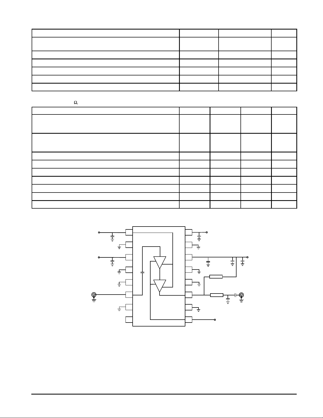
C1 – 2.7 pF
C2, C4, C8 – 100 pF
C3 – 1
µ
C5, C6 – 10 pF
F
C7 – 1000 pF
T1 – 90
T2 – 9° @ 900 MHz, Z0 = 50
BOARD MATERIAL = FR4
14
C8
13
12
11
10
9
°
@ 900 MHz, Z0 = 100
T1
T2
BIAS
Ω
C4
C2
C1
Ω
V
DD
C3
RF OUT
Figure 1. Applications Circuit Configuration
MOTOROLA RF DEVICE DATA
Page 3
TYPICAL CHARACTERISTICS
30
24
18
, OUTPUT POWER (dBm)
12
out
P
6
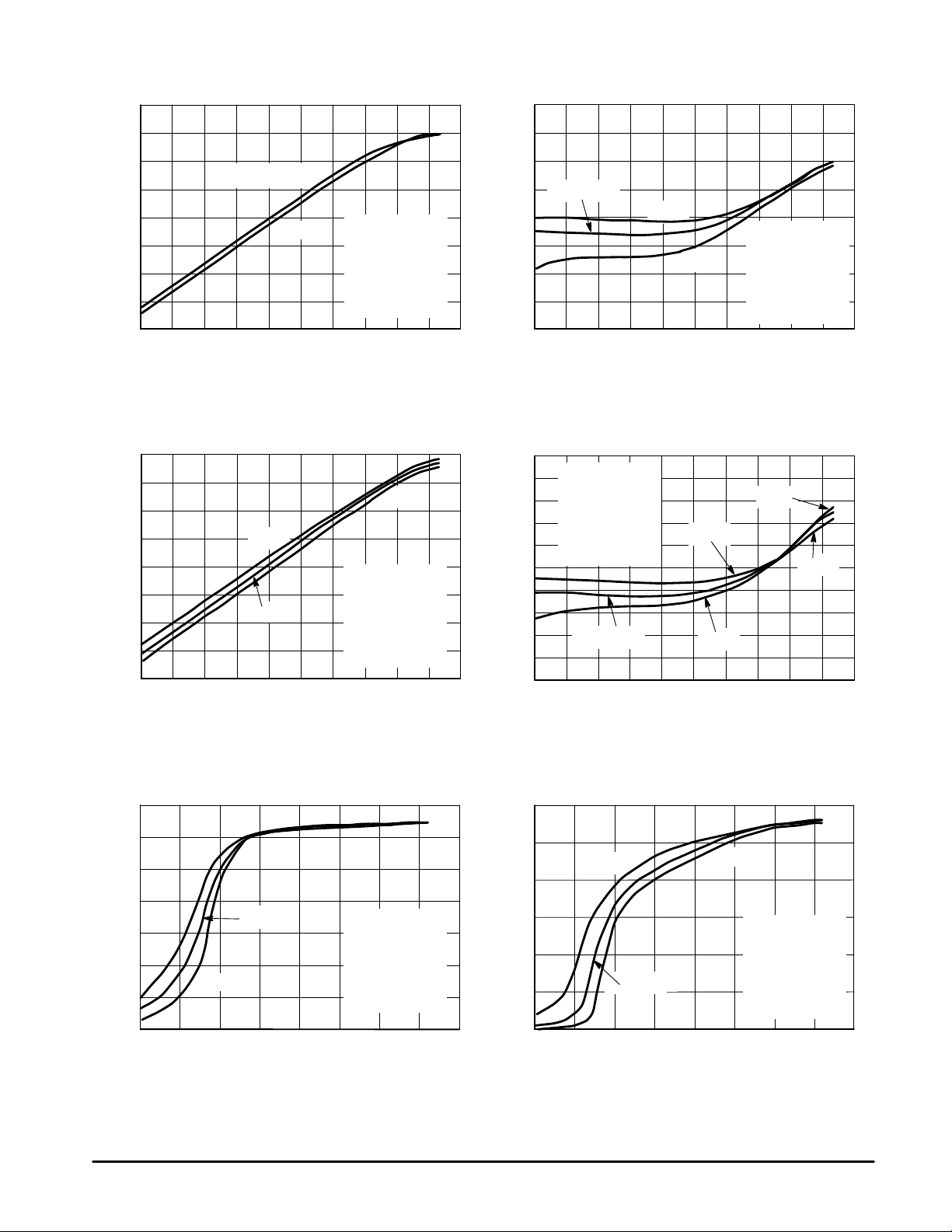
Figure 2. Output Power versus Input Power
30
24
18
, OUTPUT POWER (dBm)
12
out
P
6
Figure 4. Output Power versus Input Power
TA = 25°C, –35°C
85°C
–15–20 –10 –5 0 5
Pin, INPUT POWER (dBm)
–35°C
TA = 25°C
–15–20 –10 –5 0 5
Pin, INPUT POWER (dBm)
VDD = 3.6 V
VSS = –2.5 V
PCNTRL = 3.0 V
BIAS = 0 V
ENABLE = 3.0 V
f = 900 MHz
85°C
VDD = 4.8 V
VSS = –2.5 V
PCNTRL = 3.0 V
BIAS = 0 V
ENABLE = 3.0 V
f = 900 MHz
200
150
TA = 25°C
100
, SUPPLY CURRENT (mA)
50
DD
I
0
–15–20 –10 –5 0 5
85°C
–35°C
Pin, INPUT POWER (dBm)
Figure 3. Supply Current versus Input Power
250
VDD = 4.8 V
0
VSS = –2.5 V
PCNTRL = 3.0 V
BIAS = 0 V
ENABLE = 3.0 V
f = 900 MHz
TA = 25°C
–15–20 –10 –5 0 5
Pin, INPUT POWER (dBm)
85°C
–35°C
200
150
100
, SUPPLY CURRENT (mA)
DD
I
50
Figure 5. Supply Current versus Input Power
VDD = 3.6 V
VSS = –2.5 V
PCNTRL = 3.0 V
BIAS = 0 V
ENABLE = 3.0 V
f = 900 MHz
–35°C
85°C
30
20
10
0
–10
, OUTPUT POWER (dBm)
–20
out
P
–30
–40
0 0.5 1.0 3.0
85°C
TA = 25°C
–35°C
1.5 2.0 2.5 4.03.5
PCNTRL (VOL TS)
Figure 6. Output Power versus PCNTRL Figure 7. Supply Current versus PCNTRL
VDD = 3.6 V
VSS = –2.5 V
Pin = –2 dBm
ENABLE = 3.0 V
BIAS = 0 V
f = 900 MHz
120
100
80
60
40
, SUPPLY CURRENT (mA)
DD
I
20
85°C
TA = 25°C
0
0
0.5 1.0 3.01.5 2.0 2.5 4.03.5
PCNTRL (VOLTS)
–35°C
VDD = 3.6 V
VSS = –2.5 V
Pin = –2 dBm
ENABLE = 3.0 V
BIAS = 0 V
f = 900 MHz
MRFIC0904MOTOROLA RF DEVICE DATA
3
Page 4

TYPICAL CHARACTERISTICS
30
20
85°C
10
0
–10
, OUTPUT POWER (dBm)
out
P
–20
–30
0 0.5 1.0 3.01.5 2.0 2.5 4.03.5 4.5 5.0
–35°C
TA = 25°C
VDD = 4.8 V
VSS = –2.5 V
Pin = 0 dBm
ENABLE = 3.0 V
BIAS = 0 V
f = 900 MHz
PCNTRL (VOL TS)
Figure 8. Output Power versus PCNTRL
330
280
230
180
130
, QUIESCENT SUPPLY CURRENT (mA)
Q
DD
I
80
0.1 0.2
0 0.8 0.50 1.0 1.5
VDD = 3.6 V
4.8 V
VSS = –2.5 V
ENABLE = 3.0 V
PCNTRL = 3.0 V
°
C
TA = 25
0.3 0.4 0.5 0.6 0.7
BIAS (VOLTS)
140
120
100
80
60
40
, SUPPLY CURRENT (mA)
DD
I
20
0
0 0.5 1.0 3.01.5 2.0 2.5 4.03.5
85°C
TA = 25°C
Figure 9. Supply Current versus PCNTRL
120
100
80
60
40
, QUIESCENT SUPPLY CURRENT (mA)
20
Q
DD
I
0
–35°C
PCNTRL (VOL TS)
4.8 V
VDD = 3.6 V
PCNTRL (VOL TS)
VDD = 4.8 V
VSS = –2.5 V
Pin = 0 dBm
ENABLE = 3.0 V
BIAS = 0 V
f = 900 MHz
VSS = –2.5 V
ENABLE = 3.0 V
BIAS = 0 V
°
C
TA = 25
2.0 2.5 3.0
Figure 10. Quiescent Supply Current versus
BIAS
MRFIC0904
4
Figure 11. Quiescent Supply Current versus
PCNTRL
MOTOROLA RF DEVICE DATA
Page 5

T able 1. Scattering Parameters
f
f
(VDD = 3.6 V, VSS = –2.5 V, BIAS = 0.0 V, PCNTRL, ENABLE = 3 V, 50 Ω System)
S
f
MHz
500 0.922 –40.93 12.201 –76.39 0.002 72.64 0.276 166.48
550 0.887 –52.05 16.242 –98.58 0.002 62.03 0.276 169.80
600 0.826 –65.21 21.133 –116.66 0.003 44.52 0.297 175.47
650 0.698 –81.22 28.039 –140.66 0.004 26.65 0.342 173.06
700 0.419 –99.95 33.973 174.46 0.004 6.35 0.360 169.94
750 0.206 –106.43 32.195 145.72 0.006 –9.10 0.393 163.65
800 0.073 –56.19 31.685 121.12 0.006 –31.13 0.392 154.83
850 0.146 –4.45 29.419 85.45 0.006 –47.59 0.351 146.93
900 0.170 –1.59 25.996 64.50 0.006 –61.44 0.305 145.90
950 0.183 10.82 24.115 45.18 0.007 –80.54 0.276 152.91
1000 0.232 27.47 22.091 16.72 0.007 –107.22 0.287 162.87
1050 0.302 34.19 19.995 –5.08 0.007 –116.06 0.310 167.00
1100 0.395 34.85 17.411 –26.64 0.006 –125.77 0.337 170.51
1150 0.522 29.21 14.15 –52.28 0.006 –146.60 0.380 169.57
1200 0.607 23.25 11.961 –71.38 0.005 –154.46 0.403 167.34
1250 0.675 17.30 9.76 –88.04 0.005 –177.16 0.419 163.73
1300 0.743 9.17 7.951 –108.01 0.004 160.61 0.436 159.33
|S11| ∠ φ |S21| ∠ φ |S12| ∠ φ |S22| ∠ φ
11
S
21
S
12
S
22
T able 2. Scattering Parameters
(VDD = 4.8 V, VSS = –2.5 V, BIAS = 0.0 V, PCNTRL, ENABLE = 3 V, 50 Ω System)
S
f
MHz
500 0.910 –41.17 12.58 –78.69 0.0012 65.66 0.228 168.72
550 0.873 –51.75 17.09 –99.91 0.0024 43.49 0.232 172.87
600 0.807 –64.98 22.33 –118.28 0.0032 48.13 0.252 177.75
650 0.671 –81.03 29.24 –142.97 0.0041 17.29 0.293 174.31
700 0.409 –100.12 35.95 172.30 0.0040 –10.22 0.326 172.83
750 0.200 –104.83 34.04 143.18 0.0055 –14.65 0.349 164.57
800 0.080 –53.72 33.08 118.78 0.0056 –28.05 0.345 156.12
850 0.142 –6.52 30.64 83.58 0.0057 –45.38 0.307 147.87
900 0.165 0.32 27.22 62.36 0.0065 –62.81 0.248 146.40
850 0.187 14.68 24.95 41.95 0.0066 –86.95 0.226 146.72
1000 0.252 28.28 22.30 14.13 0.0062 –100.71 0.257 167.95
1050 0.323 32.92 20.06 –7.52 0.0057 –113.16 0.279 172.05
1100 0.409 32.35 17.37 –28.14 0.0049 –121.71 0.310 173.62
1150 0.527 26.77 14.03 –53.24 0.0051 –152.49 0.349 171.86
1200 0.606 21.18 11.89 –71.66 0.0051 –159.64 0.365 169.36
1250 0.669 15.59 9.74 –87.41 0.0043 –155.55 0.381 163.46
1300 0.735 8.10 7.96 –107.51 0.0039 171.99 0.397 161.81
|S11| ∠ φ |S21| ∠ φ |S12| ∠ φ |S22| ∠ φ
11
S
21
S
12
S
22
MRFIC0904MOTOROLA RF DEVICE DATA
5
Page 6

APPLICATIONS INFORMATION
DESIGN PHILOSOPHY
The MRFIC0904 is a versatile driver amplifier designed to
operate in the 800 MHz to 1 GHz frequency range for cellular
phone and Industrial, Scientific, and Medical (ISM) applications. The amplifier is designed using depletion mode GaAs
MESFETs to perform at high efficiency at battery voltages of
3.6 and 4.8 Volts. While designed as a driver amplifier for a
discrete transistor final stage, the device can act as a power
amplifier for lower power systems such as ISM applications
in telemetry and cordless telephones.
THEORY OF OPERATION
The MRFIC0904 has various control features making it versatile and applicable to both linear and saturated applications.
The BIAS pin allows the setting of drain quiescent current. For
non–linear applications such as GSM cellular, the pin can be
grounded. For better gain and linearity, a positive voltage up
to about 0.6 Volts can be applied. The PCNTRL pin allows
the control of the output power over a wide dynamic range
with low AM to AM distortion such as is required in GSM and
other cellular systems. As shown in Figures 6 through 9,
PCNTRL affects both the output power and the drain current
thus maintaining good efficiency over a range of output power. The ENABLE pin is used to control the on–of f state of the
device and is useful as a reduced current standby control. A
logic high signal of more than 2.5 Volts turns the device on. A
logic low signal of less than 0.5 Volts reduces total supply
current to typically less than 200 µA.
EVALUATION BOARDS
Evaluation boards are av ailable for RF Monolithic Integrated Circuits by adding a “TF” suffix to the device type.
For a complete list of currently available boards and ones
in development for newly introduced product, please con tact your local Motorola Distributor or Sales Office.
MRFIC0904
6
MOTOROLA RF DEVICE DATA
Page 7

P ACKAGE DIMENSIONS
-T-
SEATING
PLANE
-A-
NOTES:
1. DIMENSIONING AND TOLERANCING PER ANSI
916
-B-
P 8 PL
1
8
0.25 (0.010) B
M M
G
K
R X 45°
F
C
J
D
16 PL
0.25 (0.010) T B A
M
M
S S
Y14.5M, 1982.
2. CONTROLLING DIMENSION: MILLIMETER.
3. DIMENSIONS A AND B DO NOT INCLUDE
MOLD PROTRUSION.
4. MAXIMUM MOLD PROTRUSION 0.15 (0.006)
PER SIDE.
5. DIMENSION D DOES NOT INCLUDE DAMBAR
PROTRUSION. ALLOWABLE DAMBAR
PROTRUSION SHALL BE 0.127 (0.005) TOTAL
IN EXCESS OF THE D DIMENSION AT
MAXIMUM MATERIAL CONDITION.
MILLIMETERS INCHES
MIN MINMAX MAX
DIM
A
9.80
B
3.80
C
1.35
D
0.35
F
0.40
1.27 BSC 0.050 BSC
G
J
0.19
K
0.10
M
0
°
P
5.80
R
0.25
10.00
4.00
1.75
0.49
1.25
0.25
0.25
7
6.20
0.50
°
0.386
0.150
0.054
0.014
0.016
0.008
0.004
0
°
0.229
0.010
0.393
0.157
0.068
0.019
0.049
0.009
0.009
7
°
0.244
0.019
CASE 751B-05
ISSUE J
MRFIC0904MOTOROLA RF DEVICE DATA
7
Page 8

Motorola reserves the right to make changes without further notice to any products herein. Motorola makes no warranty , representation or guarantee regarding
the suitability of its products for any particular purpose, nor does Motorola assume any liability arising out of the application or use of any product or circuit,
and specifically disclaims any and all liability, including without limitation consequential or incidental damages. “T ypical” parameters can and do vary in different
applications. All operating parameters, including “T ypicals” must be validated for each customer application by customer’s technical experts. Motorola does
not convey any license under its patent rights nor the rights of others. Motorola products are not designed, intended, or authorized for use as components in
systems intended for surgical implant into the body, or other applications intended to support or sustain life, or for any other application in which the failure of
the Motorola product could create a situation where personal injury or death may occur. Should Buyer purchase or use Motorola products for any such
unintended or unauthorized application, Buyer shall indemnify and hold Motorola and its officers, employees, subsidiaries, affiliates, and distributors harmless
against all claims, costs, damages, and expenses, and reasonable attorney fees arising out of, directly or indirectly, any claim of personal injury or death
associated with such unintended or unauthorized use, even if such claim alleges that Motorola was negligent regarding the design or manufacture of the part.
Motorola and are registered trademarks of Motorola, Inc. Motorola, Inc. is an Equal Opportunity/Af firmative Action Employer.
How to reach us:
USA/ EUROPE: Motorola Literature Distribution; JAPAN: Nippon Motorola Ltd.; Tatsumi–SPD–JLDC, Toshikatsu Otsuki,
P.O. Box 20912; Phoenix, Arizona 85036. 1–800–441–2447 6F Seibu–Butsuryu–Center, 3–14–2 Tatsumi Koto–Ku, Tokyo 135, Japan. 03–3521–8315
MFAX: RMF AX0@email.sps.mot.com – T OUCHTONE (602) 244–6609 HONG KONG: Motorola Semiconductors H.K. Ltd.; 8B T a i Ping Industrial Park,
INTERNET: http://Design–NET.com 51 Ting K ok Road, T ai Po, N.T., Hong Kong. 852–26629298
MRFIC0904
8
◊
MOTOROLA RF DEVICE DATA
MRFIC0904/D
*MRFIC0904/D*
 Loading...