

Page 1
SEMICONDUCTOR TECHNICAL DATA
The MRFIC Line
The MRFIC0903 is an integrated GaAs SPDT switch designed for
transceivers operating in the 100 MHz to 2.0 GHz frequency range. The design
utilizes Motorola’s advanced GaAs RF process to yield superior performance in
a cost effective monolithic device. Applications for the MRFIC0903 include
Class 4 and 5 GSM, Class 1 and 2 DCS1800, DCS1900, DAMPS, PDC, digital
cellular systems as well as analog cellular systems.
• 2.8 W Transmitting Capability through the T ransmit Path with a 5.0 Volt
Differential Control Signal
• 1.25 W Transmitting Capability through the T ransmit Path with a 3.0 Volt
Differential Control Signal
• Single Source Operating Supply Voltage
• Low Power Consumption
• Low–Cost, Low Profile Plastic SOIC Package
• Available in Tape and Reel by Adding R2 Suffix.
R2 Suffix = 2,500 Units per Reel.
• Device Marking = M0903
Order this document
by MRFIC0903/D
ANTENNA SWITCH
GaAs MONOLITHIC
INTEGRATED CIRCUIT
CASE 751–05
(SO–8)
ABSOLUTE MAXIMUM RATINGS (T
Rating Symbol Value Unit
Supply Voltage V
Control Voltage VC1, V
Power Dissipation P
Power Input (Non–selected Port) P
Ambient Operating Temperature T
Storage Temperature T
= 25°C unless otherwise noted)
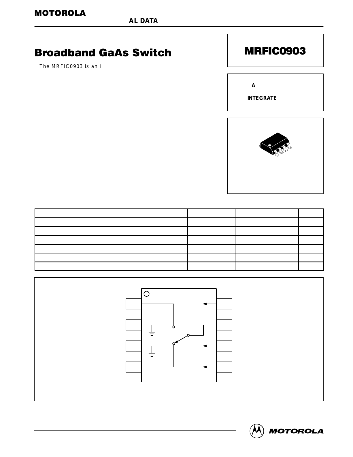
A
RF2
1
GND
2
GND
3
RF1
4
DD
D
in
A
stg
C2
10 Vdc
VDD + 0.8, VDD – 12 Vdc
1.0 W
0.325 W
–35 to +85 °C
–65 to +150 °C
V
8
C2
RFC
7
V
6
DD
V
5
C1
REV 1
Motorola, Inc. 1997
Pin Connections and Functional Block Diagram
MRFIC0903MOTOROLA RF DEVICE DATA
1
Page 2
RECOMMENDED OPERATING RANGES
Parameter Symbol Value Unit
Supply Voltage V
Control Voltage Range VC1, V
RF Frequency Range f
DD
C2VDD
RF
0 to 5.0 Vdc
– 5.0 to VDD + 0.5 Vdc
100 to 2000 MHz
ELECTRICAL CHARACTERISTICS (V
Characteristic Min Typ Max Unit
Supply Current
I
DD
I
Control
VSWR
Insertion Loss (RFC/RF1, RFC/RF2)
Isolation (RFC/RF2, RFC/RF1)
Output Power at 0.1 dB Compression — 34.5 — dBm
Electrical Characteristics at 900 MHz measured in test circuit schematic shown in Figure 1 with board losses removed.
ELECTRICAL CHARACTERISTICS (V
Characteristic Min Typ Max Unit
Supply Current
I
DD
I
Control
VSWR
Insertion Loss (RFC/RF1, RFC/RF2)
Isolation (RFC/RF2, RFC/RF1)
Output Power at 0.1 dB Compression — 34 — dBm
Electrical Characteristics at 1800 MHz measured in test circuit schematic shown in Figure 2 with board losses removed.
= 5.0 V, Pin = 2.5 W (34 dBm), f = 900 MHz, TA = 25°C unless otherwise noted)
DD
—
—
—
—
18
= 5.0 V, Pin = 2.0 W (33 dBm), f = 1800 MHz, TA = 25°C unless otherwise noted)
DD
—
—
—
—
18
100
150
1.5:1
0.55
20
100
150
1.5:1
0.7
20
170
300
—
0.8
—
170
300
—
0.85
—
µA
µA
dB
dB
µA
µA
dB
dB
VC1 and VC2 Input Voltage
High V
Low VDD – 10 — VDD – 5 Vdc
V
C1
High Low Insertion Loss Isolation
Low High Isolation Insertion Loss
Min Typ Max Unit
DD
V
C2
— VDD + 0.5 Vdc
RFC – RF1 RFC – RF2
T able 1. Logic Levels
MRFIC0903
2
MOTOROLA RF DEVICE DATA
Page 3
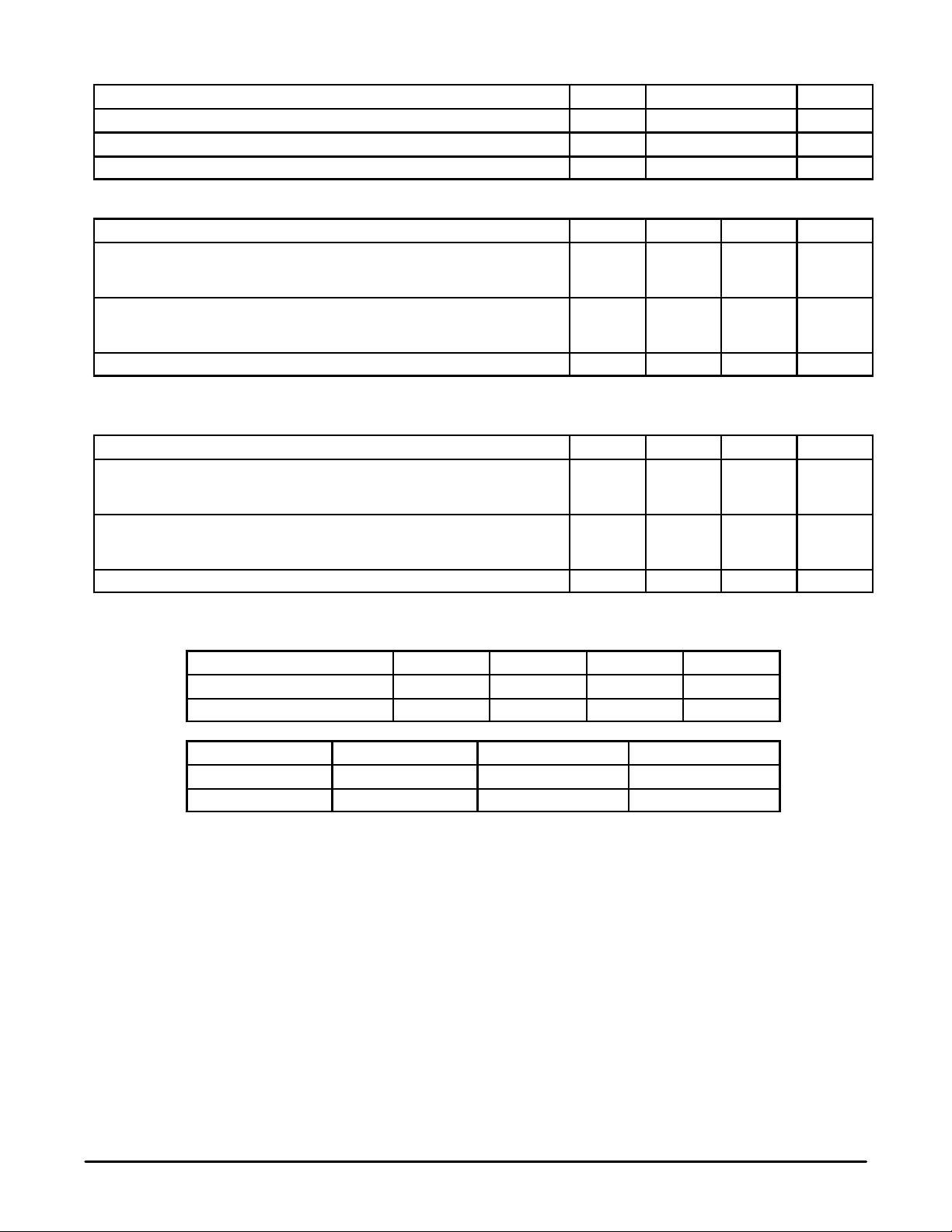
RF1
50
Ω
+
V
C1
–
C1
5
4
TL1 C2
+
V
DD
–
RFC
Ω
50
V
C2
C1, C5 — 2.7 pF, Chip Capacitor
C2, C4, C6 — 100 pF , Chip Capacitor
C3 — 10 pF, Chip Capacitor
Note: Decoupling capacitors on pins 5, 6 and 8 must be as close as possible to the pins.
C4 TL2
+
–
C3
C5
6
DUT
7
8
3
2
1
TL3 C6
TL1, TL3 — 12 degrees of 50 Ω line at 1 GHz
TL2 — 15 degrees of 50 Ω line at 1 GHz
Figure 1. 300 MHz to 1600 MHz Test Circuit Configuration
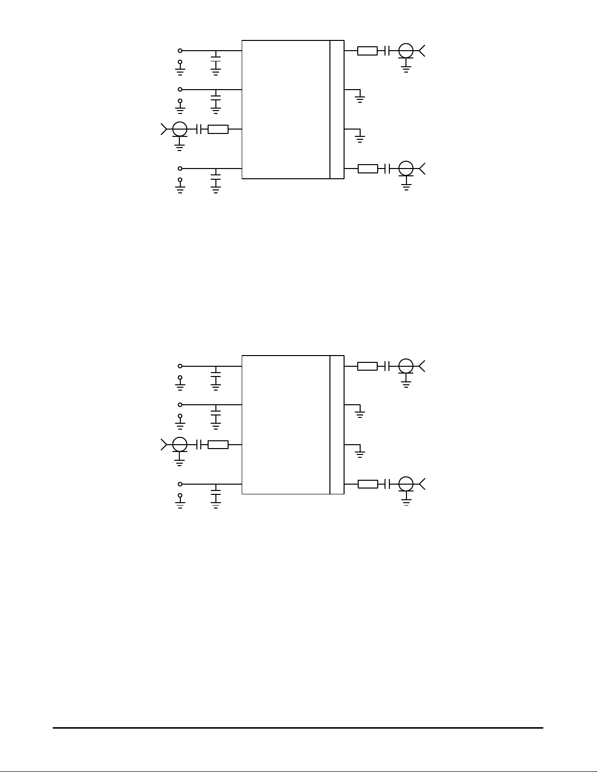
+
V
C1
–
C1
5
4
TL1 C2
RF2
50
RF1
50
Ω
Ω
+
V
DD
–
RFC
Ω
50
V
C2
C1, C5 — 1.3 pF, Chip Capacitor
C2, C3, C4, C6 — 8.2 pF , Chip Capacitor
Note: Decoupling capacitors on pins 5, 6 and 8 must be as close as possible to the pins.
C4 TL2
+
–
C3
C5
6
DUT
7
8
3
2
1
TL3 C6
TL1, TL3 — 12 degrees of 50 Ω line at 1 GHz
TL2 — 15 degrees of 50 Ω line at 1 GHz
Figure 2. 1600 MHz to 2000 MHz T est Circuit Configuration
RF2
50
Ω
MRFIC0903MOTOROLA RF DEVICE DATA
3
Page 4

TYPICAL CHARACTERISTICS
1
0.8
TA = 25°C
0.6
85°C
0.4
IL, INSERTION LOSS (dB)
0.2
0
2.5 5 7.5 10
–35°C
f = 900 MHz
VDD, SUPPLY VOLT AGE (VOLTS)
Figure 3. Insertion Loss at 0.1 dB
Compression versus Supply V oltage
37
35
85°C
33
TA = 25°C
–35°C
22
21.5
21
ISOL, ISOLATION (dB)
20.5
20
2.5 5 7.5 10
TA = 25, 85°C
–35°C
f = 900 MHz
VDD, SUPPLY VOLT AGE (VOLTS)
Figure 4. Isolation at 0.1 dB
Compression versus Supply V oltage
37
35
–35°C
33
85°C
TA = 25°C
31
, INPUT POWER (dBm)
in
P
29
f = 900 MHz
27
2.5 5 7.5 10
VDD, SUPPLY VOLT AGE (VOLTS)
Figure 5. Input Power at 0.1 dB
Compression versus Supply V oltage
1
0.75
TA = 25°C
0.5
–35°C
0.25
DISS
P , DISSIP ATED POWER (W)
0
2.5 5 7.5 10
VDD, SUPPLY VOLT AGE (VOLTS)
85°C
f = 900 MHz
31
out
P , OUTPUT POWER (dBm)
29
f = 900 MHz
27
2.5 5 7.5 10
VDD, SUPPLY VOLT AGE (VOLTS)
Figure 6. Output Power at 0.1 dB
Compression versus Supply V oltage
0.3
0.4
0.3
0.2
, SUPPLY CURRENT (mA)
DD
I
0.1
0
2.5 5 7.5 10
VDD, SUPPLY VOLT AGE (VOLTS)
–35°C
85°C
TA = 25°C
MRFIC0903
4
Figure 7. Dissipated Power at 0.1 dB
Compression versus Supply V oltage
Figure 8. Supply Current at 0.1 dB
Compression versus Supply V oltage
MOTOROLA RF DEVICE DATA
Page 5

TYPICAL CHARACTERISTICS
2
1.5
1
0.5
Ivc, CONTROL CURENT (mA)
0
2.5 5 7.5 10
VDD, SUPPLY VOLT AGE (VOLTS)
TA = –35° to + 85°C
Figure 9. Control Current at Vc Pins at 0.1 dB
Compression versus Supply V oltage
23
85°C
22
TA = 25°C
21
ISOL, ISOLATION (dB)
20
19
2.5 5 7.5 10
–35°C
f = 1800 MHz
VDD, SUPPLY VOLT AGE (VOLTS)
1
85°C
0.8
0.6
0.4
IL, INSERTION LOSS (dB)
0.2
0
2.5 5 7.5 10
VDD, SUPPLY VOLT AGE (VOLTS)
TA = 25°C
–35°C
f = 1800 MHz
Figure 10. Insertion Loss at 0.1 dB
Compression versus Supply V oltage
37
TA = 25°C
35
33
31
, INPUT POWER (dBm)
in
P
85°C
29
27
2.5 5 7.5 10
VDD, SUPPLY VOLT AGE (VOLTS)
–35°C
f = 1800 MHz
Figure 11. Isolation at 0.1 dB
Compression versus Supply V oltage
37
35
–35°C
33
31
out
P , OUTPUT POWER (dBm)
29
27
2.5 5 7.5 10
85°C
VDD, SUPPLY VOLT AGE (VOLTS)
TA = 25°C
f = 1800 MHz
Figure 13. Output Power at 0.1 dB
Compression versus Supply V oltage
Figure 12. Input Power at 0.1 dB
Compression versus Supply V oltage
1
0.75
0.5
0.25
DISS
P , DISSIP ATED POWER (W)
0
2.5 5 7.5 10
VDD, SUPPLY VOLT AGE (VOLTS)
85°C
TA = 25°C
–35°C
f = 1800 MHz
Figure 14. Dissipated Power at 0.1dB
Compression versus Supply V oltage
MRFIC0903MOTOROLA RF DEVICE DATA
5
Page 6

TYPICAL CHARACTERISTICS
2
VDD = 5 Vdc
Pin = 4 dBm
1.5
1
IL, INSERTION LOSS (dB)
0.5
0
100
TA = 25°C
600 1100 160
f, FREQUENCY (MHz)
85°C
–35°C
210
0
Figure 15. Insertion Loss versus Frequency Figure 16. Input Return Loss
APPLICATIONS INFORMATION
DESIGN INFORMATION
The MRFIC0903 SPDT antenna switch was designed for
low cost, flexibility and ease of use. This is accomplished by
its internal topology that allows control of the switch through
its TTL/CMOS compatible (0 to VDD) control pins. Operating
on a single positive supply, the switch was designed for a
minimum supply voltage, minimum power consumption and
low current TTL/CMOS compatible control signals.
THEORY OF OPERATION
The MRFIC0903 can be used as a transmit and receive or
antenna diversity switch in the frequency range from
100 MHz to 2 GHz with incident power levels as high as
4 watts.
The frequency behavior can be optimized by resonating
the DC blocking capacitor’s position and value with the parasitic inductance of the package lead. Operation from 300
MHz to 1.6 GHz can be optimized with a high Q 100 pF
blocking capacitor. For the higher frequency band from 1.6
GHz to 2.0 GHz, a 8.2 pF capacitor is suggested. Further improvements can be achieved by resonating the inductance of
VDD, VC1, and VC2 pins with the appropriate capacitor values.
The power handling capability and linearity of the
MRFIC0903 is dependent only on the supply voltage. With a
3 V supply, the device handles 1.25 W (1.6 W PEP) of
incident power while maintaining good linearity and low
harmonic distortion. The power transmitting capability increases to 3 W of incident power with a 5 V supply and up to
4 W with a 7.5 V supply .
18
16
14
TA = 25°C
12
10
RL, INPUT RETURN LOSS (dB)
8
0
100 600 1100 160
f, FREQUENCY (MHz)
versus Frequency
Due to the device’s inherently low harmonic distortion, the
switch requires little harmonic filtering at its outputs. It also
has a high reverse third–order intercept point for use in non–
TDMA antenna diversity applications (analog cellular systems).
BIASING CONSIDERATIONS
The MRFIC0903 is based on a floating “cold FET” topology. With this topology, the differential voltage between V
and VC2 dictates the power handling capability. For example, the device’s power handling capability is the same with
the device biased with 5 V at VC1 and 0 V at VC2, with 0 V at
VC1 and –5 V at VC2, or with 3 V at VC1 and –2 V at VC2.
POSSIBLE APPLICATIONS
The MRFIC0903 can be used in a number of cellular and
cordless phone applications. The part is applicable for analog cellular phones in systems such as AMPS, TACS,
NAMPS, ETACS and NMT900; for digital cellular phones in
systems such as GSM, PDC, DAMPS, DCS1800, PCS and
NADC; and for cordless phones in systems such as DECT,
PHS, ISM, CT1 and CT2. In general it can fit into any application where high power handling capability is required for
frequencies ranging from 100 MHz to 2 GHz.
EVALUATION BOARDS
Evaluation boards are available for RF Monolithic Integrated Circuits by adding a “TF” suffix to the device type.
For a complete list of currently available boards and ones
in development for newly introduced product, please con tact your local Motorola Distributor or Sales Office.
–35°C
VDD = 5 Vdc
Pin = 4 dBm
0
85°C
210
0
C1
MRFIC0903
6
MOTOROLA RF DEVICE DATA
Page 7

P ACKAGE DIMENSIONS
C
A
A1
D
58
0.25MB
E
1
B
e
H
4
M
h
X 45
_
q
C
A
SEATING
PLANE
0.10
L
B
SS
A0.25MCB
NOTES:
1. DIMENSIONING AND TOLERANCING PER ASME
Y14.5M, 1994.
2. DIMENSIONS ARE IN MILLIMETERS.
3. DIMENSION D AND E DO NOT INCLUDE MOLD
PROTRUSION.
4. MAXIMUM MOLD PROTRUSION 0.15 PER SIDE.
5. DIMENSION B DOES NOT INCLUDE MOLD
PROTRUSION. ALLOWABLE DAMBAR
PROTRUSION SHALL BE 0.127 TOTAL IN EXCESS
OF THE B DIMENSION AT MAXIMUM MATERIAL
CONDITION.
MILLIMETERS
DIM MIN MAX
A 1.35 1.75
A1 0.10 0.25
B 0.35 0.49
C 0.18 0.25
D 4.80 5.00
E
3.80 4.00
1.27 BSCe
H 5.80 6.20
h
0.25 0.50
L 0.40 1.25
0 7
q
__
CASE 751–05
ISSUE S
MRFIC0903MOTOROLA RF DEVICE DATA
7
Page 8

Motorola reserves the right to make changes without further notice to any products herein. Motorola makes no warranty , representation or guarantee regarding
the suitability of its products for any particular purpose, nor does Motorola assume any liability arising out of the application or use of any product or circuit, and
specifically disclaims any and all liability, including without limitation consequential or incidental damages. “T ypical” parameters which may be provided in Motorola
data sheets and/or specifications can and do vary in different applications and actual performance may vary over time. All operating parameters, including “Typicals”
must be validated for each customer application by customer’s technical experts. Motorola does not convey any license under its patent rights nor the rights of
others. Motorola products are not designed, intended, or authorized for use as components in systems intended for surgical implant into the body, or other
applications intended to support or sustain life, or for any other application in which the failure of the Motorola product could create a situation where personal injury
or death may occur. Should Buyer purchase or use Motorola products for any such unintended or unauthorized application, Buyer shall indemnify and hold Motorola
and its officers, employees, subsidiaries, affiliates, and distributors harmless against all claims, costs, damages, and expenses, and reasonable attorney fees
arising out of, directly or indirectly, any claim of personal injury or death associated with such unintended or unauthorized use, even if such claim alleges that
Motorola was negligent regarding the design or manufacture of the part. Motorola and are registered trademarks of Motorola, Inc. Motorola, Inc. is an Equal
Opportunity/Affirmative Action Employer.
How to reach us:
USA/EUROPE/Locations Not Listed: Motorola Literature Distribution; JAPAN: Nippon Motorola Ltd.: SPD, Strategic Planning Office, 4–32–1,
P.O. Box 5405, Denver, Colorado 80217. 303–675–2140 or 1–800–441–2447 Nishi–Gotanda, Shinagawa–ku, Tokyo 141, Japan. 81–3–5487–8488
Mfax: RMFAX0@email.sps.mot.com – TOUCHTONE 602–244–6609 ASIA/P ACIFIC: Motorola Semiconductors H.K. Ltd.; 8B Tai Ping Industrial Park,
– US & Canada ONLY 1–800–774–1848 51 Ting Kok Road, T ai Po, N.T., Hong Kong. 852–26629298
INTERNET: http://motorola.com/sps
Mfax is a trademark of Motorola, Inc.
MRFIC0903
8
◊
MOTOROLA RF DEVICE DATA
MRFIC0903/D
 Loading...