

Page 1
SEMICONDUCTOR TECHNICAL DATA
Order this document
by MRF927T1/D
The RF Small Signal Line
$ "
$ # " $ !
#% !!" !
Designed for use in low voltage, low current applications at frequencies to
2.0 GHz. Specifically aimed at portable communication devices such as
pagers and hand–held phones.
• High Gain (G
• Small, Surface–Mount Package (SC–70)
• High Current Gain–Bandwidth Product at Low Current,
Low Voltage (fτ = 8.0 GHz Typ @ 3.0 V, 5.0 mA)
• Available in Tape and Reel by Adding T1 or T3 Suffix to Part Number.
T1 Suffix = 3,000 Units per 8 mm, 7 inch Reel.
T3 Suffix = 10,000 Units per 8 mm, 7 inch Reel.
15 dB Typ @ 1.0 GHz) @ 1.0 mA
Umax
IC = 10 mA
LOW NOISE
HIGH FREQUENCY
TRANSISTOR
CASE 419–02, STYLE 3
(SC–70/SOT–323)
MAXIMUM RATINGS
Rating Symbol Value Unit
Collector–Emitter Voltage V
Collector–Base Voltage V
Emitter–Base Voltage V
Collector Current — Continuous I
Total Device Dissipation @ TC = 50°C
Derate above 50°C
Storage Temperature Range T
Operating Temperature Range T
THERMAL CHARACTERISTICS
Characteristic Symbol Value Unit
Thermal Resistance, Junction–to–Case R
DEVICE MARKING
MRF927T1 = F
CEO
CBO
EBO
C
P
D
stg
J
θJC
10 Vdc
20 Vdc
2.5 Vdc
10 mAdc
100
1.0
– 55 to +150 °C
150 °C
1000 °C/W
mW
mW/°C
REV 1
Motorola, Inc. 1997
MRF927T1 MRF927T3MOTOROLA RF DEVICE DATA
1
Page 2
ELECTRICAL CHARACTERISTICS (T
Characteristic
OFF CHARACTERISTICS
Collector–Emitter Breakdown Voltage
(IC = 0.1 mA, IB = 0 mA)
Collector–Base Breakdown Voltage
(IC = 0.1 mA, IE = 0)
Emitter–Base Breakdown Voltage
(IE = 0.1 mA, IC = 0)
Emitter Cutoff Current
(VEB = 1.0 Vdc, IC = 0)
ON CHARACTERISTICS
DC Current Gain
(VCE = 1.0 Vdc, IC = 0.5 mA)
DYNAMIC CHARACTERISTICS
Collector–Base Capacitance
(VCB = 1.0 Vdc, IE = 0, f = 1.0 MHz)
Current–Gain Bandwidth Product
(VCE = 3.0 Vdc, IE = 5.0 mA, f = 1.0 GHz)
PERFORMANCE CHARACTERISTICS
Noise Figure — Minimum
(VCE = 1.0 Vdc, IC = 1.0 mA, f = 1000 MHz) Figure 3
Associated Gain at Minimum Noise Figure
(VCE = 1.0 Vdc, IC = 1.0 mA, f = 1000 MHz) Figure 3
Maximum Unilateral Gain
(VCE = 1.0 Vdc, IC = 1.0 mA, f = 1000 MHz)
Insertion Gain
(VCE = 1.0 Vdc, IC = 1.0 mA, f = 1000 MHz)
Noise Resistance
(VCE = 1.0 Vdc, IC = 1.0 mA, f = 1000 MHz)
= 25°C unless otherwise noted)
C
Symbol Min Typ Max Unit
V
(BR)CEO
V
(BR)CBO
V
(BR)EBO
I
EBO
h
FE
C
cb
f
τ
NF
min
G
NF
G
Umax
2
|S
| — 8.0 — dB
21
R
N
10 — — Vdc
20 — — Vdc
1.5 — — Vdc
— — 0.1 µA
50 — 200 —
— 0.33 — pF
— 8.0 — GHz
— 1.7 — dB
— 9.8 — dB
— 15 — dB
— 62 — Ohms
MRF927T1 MRF927T3
2
MOTOROLA RF DEVICE DATA
Page 3
TYPICAL CHARACTERISTICS
0.5
0.45
0.4
0.35
0.3
0.25
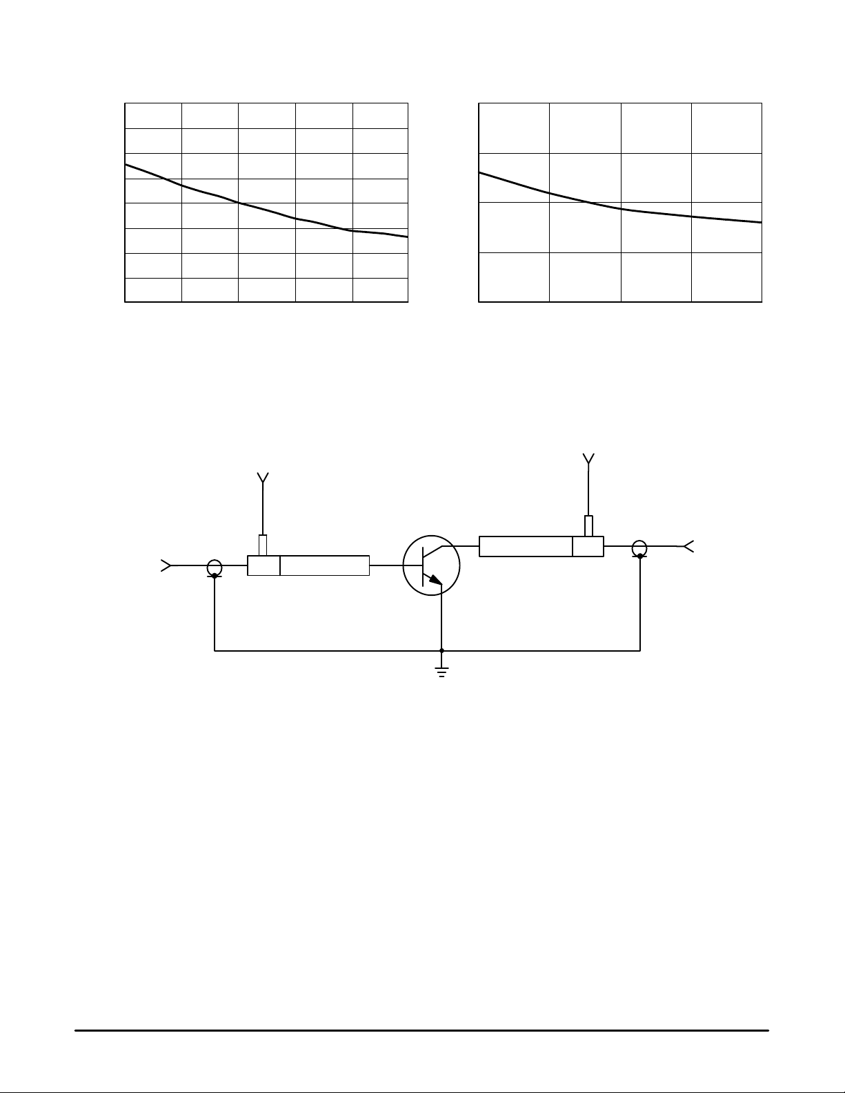
C, CAPACITANCE (pF)
0.2
0.15
0.1
VEB, EMITTER–BASE VOLTAGE (VOLTS)
Figure 1. Cib Input Capacitance versus V oltage
V
BE
0.4
0.35
0.3
C, CAPACITANCE (pF)
0.25
1.61.31.00.70.40
0.2
8.06.04.02.01.0
VCB, REVERSE VOLTAGE (VOLTS)
Figure 2. Ccb, Collector–Base
Capacitance versus V oltage
V
CE
RF INPUT
NETWORK
DUT
**SLUG TUNER*BIAS
Figure 3. Functional Circuit Schematic
**SLUG TUNER
*BIAS
NETWORK
RF OUTPUT
*HP11590B
**MICROLAB/FXR
**SF – 11N < 1 GHz
**SF – 31IN
≥
1 GHz
MRF927T1 MRF927T3MOTOROLA RF DEVICE DATA
3
Page 4
TYPICAL CHARACTERISTICS
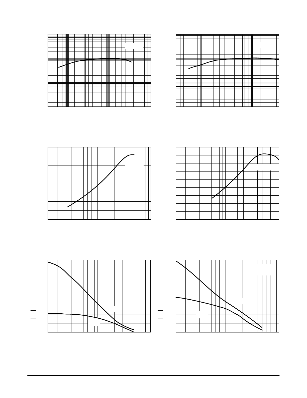
1000
100
, DC CURRENT GAIN
10
FE
h
T
f , GAIN BANDWIDTH PRODUCT (GHz)
1000
VCE = 1 V
100
, DC CURRENT GAIN
10
FE
h
1
IC, COLLECTOR CURRENT (mA)
1001010.10.010.001
Figure 4. DC Current Gain versus
Collector Current
8
7
6
5
4
3
2
1
0
IC, COLLECTOR CURRENT (mA)
VCE = 1 V
4 103210.5
53210.50.25
100.1 0.1
T
f , GAIN BANDWIDTH PRODUCT (GHz)
1
IC, COLLECTOR CURRENT (mA)
Figure 5. DC Current Gain versus
Collector Current
9
7
6
5
4
3
2
1
0
IC, COLLECTOR CURRENT (mA)
VCE = 3 V
1010.10.010.001
VCE = 3 V
485
Figure 6. Gain Bandwidth Product versus
40
35
30
25
20
15
, INSERTION GAIN (dB)
2
21
10
S
, MAXIMUM UNILATERAL GAIN (dB)
5
Umax
G
0
0.30.1
Figure 8. Forward Insertion Gain and Maximum
Unilateral Gain versus Frequency
MRF927T1 MRF927T3
4
Collector Current
VCE = 1 V
IC = 1 mA
G
Umax
2
|S21|
0.5 0.7 2 3 4 5
f, FREQUENCY (GHz)
1 10 0.3 0.5 0.7 1 10
Figure 7. Gain Bandwidth Product versus
40
35
30
25
20
15
, INSERTION GAIN (dB)
2
21
10
S
, MAXIMUM UNILATERAL GAIN (dB)
5
Umax
G
0
0.1
Figure 9. Forward Insertion Gain and Maximum
Collector Current
VCE = 3 V
IC = 3 mA
G
Umax
2
|S21|
2345
f, FREQUENCY (GHz)
Unilateral Gain versus Frequency
MOTOROLA RF DEVICE DATA
Page 5

TYPICAL CHARACTERISTICS
20
18
16
14
12
10
8
, ASSOCIATED GAIN (dB)
6
NF
G
4
2
0
Figure 10. Minimum Noise Figure and
Associated Gain versus Frequency
25
20
15
10
MSG, MAG (dB)
5
G
NF
NF
min
f, FREQUENCY (MHz)
MSG
VCE = 1 V
IC = 0.5 mA
1500
VCE = 1 V
IC = 1 mA
MAG
20
18
16
14
3
2.5
2
1.5
1
0.5
0
20001000900700500300
12
10
8
, ASSOCIATED GAIN (dB)
6
, MINIMUM NOISE FIGURE (dB)
NF
G
4
min
NF
2
0
Figure 11. Minimum Noise Figure and
30
25
20
15
MSG, MAG (dB)
10
5
VCE = 1 V
IC = 1 mA
G
NF
NF
min
f, FREQUENCY (MHz)
Associated Gain versus Frequency
VCE = 3 V
IC = 3 mA
MSG
MAG
1500
3
2.5
2
1.5
, MINIMUM NOISE FIGURE (dB)
1
min
NF
0.5
0
20001000900700500300
0
0.3 0.5 0.70.1 0.3 0.5
0.70.1
110 10
f, FREQUENCY (GHz)
2345 1 2345
Figure 12. MSG, Maximum Stable Gain;
MAG, Maximum Available Gain versus Frequency
4
3.5
3
2.5
2
1.5
, MINIMUM NOISE FIGURE (dB)
1
min
NF
0.5
0
0.1 10
IC, COLLECTOR CURRENT (mA)
Figure 14. Noise Figure and Gain @ Minimum
Noise Figure versus Collector Current
0
f, FREQUENCY (GHz)
Figure 13. MSG, Maximum Stable Gain;
MAG, Maximum Available Gain versus Frequency
VCE = 1 V
G
NF
NF
min
3210.50.25
16
14
12
10
8
6
, ASSOCIATED GAIN (dB)
NF
4
G
2
0
MRF927T1 MRF927T3MOTOROLA RF DEVICE DATA
5
Page 6

S
V
CE
I
C
f
V
CE
(Vdc)
1.0 0.25 0.10 0.992 –4 0.911 174 0.020 86 0.997 –3
I
C
(mA)
0.5 0.10 0.983 –5 1.788 174 0.020 86 0.994 –3
1.0 0.10 0.965 –7 3.383 172 0.020 85 0.990 –4
f
(GHz)
0.20 0.990 –9 0.903 169 0.039 83 0.993 –6
0.30 0.983 –13 0.909 163 0.059 80 0.992 –8
0.40 0.978 –17 0.904 157 0.077 77 0.988 –11
0.50 0.973 –21 0.834 149 0.095 72 0.975 –13
0.60 0.943 –25 0.892 144 0.111 69 0.966 –16
0.70 0.929 –29 0.873 139 0.127 66 0.958 –19
0.80 0.889 –33 0.901 135 0.142 63 0.949 –22
0.90 0.895 –37 0.888 129 0.158 60 0.939 –24
1.00 0.876 –41 0.890 124 0.171 57 0.929 –26
1.50 0.772 –60 0.871 100 0.227 44 0.873 –38
2.00 0.670 –78 0.835 80 0.261 34 0.823 –48
2.50 0.564 –96 0.812 62 0.276 25 0.776 –58
3.00 0.477 –114 0.785 48 0.276 18 0.741 –68
3.50 0.412 –132 0.741 36 0.270 15 0.722 –77
4.00 0.364 –151 0.701 25 0.261 14 0.711 –87
4.50 0.308 –172 0.702 17 0.261 18 0.682 –97
5.00 0.297 –166 0.639 11 0.270 22 0.686 –107
0.20 0.977 –10 1.763 168 0.040 82 0.992 –7
0.30 0.965 –16 1.764 162 0.059 79 0.984 –10
0.40 0.953 –21 1.735 156 0.077 76 0.976 –13
0.50 0.947 –26 1.637 147 0.094 70 0.954 –16
0.60 0.901 –30 1.673 142 0.109 67 0.941 –19
0.70 0.878 –34 1.619 137 0.124 64 0.927 –21
0.80 0.827 –38 1.601 132 0.136 62 0.912 –24
0.90 0.825 –43 1.594 127 0.151 58 0.893 –27
1.00 0.796 –48 1.571 122 0.162 56 0.877 –29
1.50 0.659 –67 1.420 99 0.207 45 0.797 –40
2.00 0.535 –85 1.275 80 0.232 37 0.733 –49
2.50 0.417 –102 1.177 63 0.247 32 0.678 –58
3.00 0.332 –122 1.097 50 0.256 29 0.639 –67
3.50 0.271 –143 1.014 38 0.265 28 0.617 –75
4.00 0.238 –164 0.949 28 0.279 29 0.604 –84
4.50 0.212 170 0.928 19 0.305 31 0.573 –94
5.00 0.218 147 0.856 12 0.333 31 0.574 –105
0.20 0.952 –14 3.315 165 0.040 81 0.982 –9
0.30 0.928 –20 3.277 157 0.057 77 0.965 –13
0.40 0.905 –26 3.172 151 0.074 73 0.947 –16
0.50 0.88 –33 3.027 141 0.090 67 0.910 –19
0.60 0.819 –37 2.936 136 0.102 64 0.887 –23
0.70 0.783 –42 2.804 130 0.115 61 0.861 –26
0.80 0.725 –47 2.666 125 0.125 59 0.839 –28
0.90 0.702 –52 2.623 119 0.136 56 0.810 –31
1.00 0.664 –57 2.525 114 0.145 54 0.787 –33
1.50 0.504 –75 2.085 93 0.181 47 0.690 –42
2.00 0.382 –92 1.759 75 0.207 42 0.626 –50
2.50 0.278 –108 1.548 61 0.229 40 0.577 –58
3.00 0.21 –129 1.397 48 0.252 38 0.543 –66
3.50 0.168 –154 1.271 38 0.276 36 0.523 –73
4.00 0.15 –177 1.177 28 0.303 35 0.513 –82
4.50 0.148 –155 1.123 19 0.336 34 0.490 –91
5.00 0.165 –132 1.049 12 0.369 32 0.487 –101
|S11|
11
éĂφ
|S21|
S
21
éĂφ
|S12|
S
12
éĂφ
|S22|
S
22
éĂφ
T able 1. Common Emitter S–Parameters
MRF927T1 MRF927T3
MOTOROLA RF DEVICE DATA
6
Page 7

S
V
CE
I
C
f
V
CE
I
C
f
V
CE
(Vdc)
1.0 2.0 0.10 0.928 –10 6.181 169 0.020 83 0.980 –6
I
C
(mA)
f
(GHz)
0.20 0.901 –19 5.967 160 0.037 78 0.959 –12
0.30 0.856 –28 5.744 150 0.054 73 0.923 –17
0.40 0.811 –36 5.410 142 0.068 69 0.886 –22
0.50 0.753 –43 5.051 132 0.080 63 0.828 –25
0.60 0.681 –48 4.679 126 0.091 61 0.790 –28
0.70 0.632 –54 4.367 119 0.100 59 0.753 –31
0.80 0.574 –59 4.021 114 0.108 57 0.726 –33
0.90 0.538 –64 3.831 109 0.116 55 0.692 –35
1.00 0.497 –68 3.595 104 0.123 54 0.667 –37
1.50 0.349 –86 2.732 85 0.156 50 0.576 –44
2.00 0.255 –102 2.200 70 0.186 47 0.527 –50
2.50 0.182 –120 1.871 57 0.216 45 0.491 –58
3.00 0.137 –143 1.647 46 0.246 42 0.469 –66
3.50 0.115 –167 1.478 36 0.276 39 0.460 –73
4.00 0.109 –167 1.356 27 0.306 36 0.453 –81
4.50 0.115 –138 1.268 19 0.337 33 0.443 –89
5.00 0.136 –119 1.190 11 0.368 30 0.441 –98
|S11|
11
éĂφ
|S21|
S
21
éĂφ
|S12|
S
12
éĂφ
|S22|
S
22
T able 1. Common Emitter S–Parameters (continued)
éĂφ
S
V
CE
(Vdc)
3.0 0.5 0.10 0.985 –5 1.796 174 0.018 86 0.995 –3
I
C
(mA)
1.0 0.10 0.969 –6 3.341 173 0.017 85 0.992 –4
f
(GHz)
0.20 0.980 –10 1.776 169 0.034 83 0.993 –6
0.30 0.969 –15 1.778 163 0.051 79 0.986 –9
0.40 0.959 –19 1.753 157 0.066 76 0.980 –12
0.50 0.952 –24 1.651 149 0.081 71 0.961 –14
0.60 0.910 –28 1.693 144 0.095 68 0.949 –17
0.70 0.888 –32 1.639 139 0.108 65 0.937 –20
0.80 0.841 –36 1.628 134 0.119 63 0.924 –23
0.90 0.839 –41 1.618 129 0.131 60 0.908 –25
1.00 0.812 –45 1.596 124 0.142 57 0.894 –27
1.50 0.681 –64 1.445 102 0.184 47 0.824 –38
2.00 0.565 –80 1.294 83 0.210 39 0.768 –47
2.50 0.455 –96 1.190 66 0.226 33 0.720 –56
3.00 0.369 –112 1.106 53 0.237 30 0.687 –64
3.50 0.308 –128 1.019 41 0.246 28 0.670 –72
4.00 0.264 –146 0.950 30 0.256 28 0.661 –81
4.50 0.212 –166 0.933 21 0.274 29 0.638 –89
5.00 0.201 –171 0.858 13 0.294 30 0.642 –99
0.20 0.958 –13 3.284 166 0.034 81 0.985 –8
0.30 0.938 –19 3.255 159 0.050 78 0.972 –11
0.40 0.917 –24 3.163 152 0.064 74 0.957 –15
0.50 0.896 –30 3.019 143 0.078 68 0.925 –18
0.60 0.838 –35 2.951 138 0.089 66 0.905 –21
0.70 0.805 –40 2.823 132 0.101 63 0.883 –23
0.80 0.750 –44 2.700 127 0.110 61 0.864 –26
0.90 0.732 –49 2.661 122 0.121 58 0.838 –28
1.00 0.696 –53 2.570 117 0.129 56 0.818 –31
1.50 0.541 –71 2.139 95 0.163 48 0.731 –40
2.00 0.424 –86 1.807 78 0.188 43 0.674 –47
2.50 0.325 –100 1.588 63 0.210 40 0.629 –55
3.00 0.252 –116 1.430 51 0.230 37 0.600 –63
3.50 0.204 –132 1.294 40 0.250 36 0.589 –70
4.00 0.170 –150 1.195 30 0.272 34 0.581 –78
4.50 0.136 –173 1.141 21 0.297 33 0.565 –86
5.00 0.134 –162 1.063 13 0.323 32 0.566 –95
|S11|
11
éĂφ
|S21|
S
21
éĂφ
|S12|
S
12
éĂφ
|S22|
S
22
éĂφ
T able 2. Common Emitter S–Parameters
MRF927T1 MRF927T3MOTOROLA RF DEVICE DATA
7
Page 8

S
V
CE
I
C
f
V
CE
(Vdc)
3.0 3.0 0.10 0.902 –11 8.541 168 0.017 83 0.976 –7
I
C
(mA)
5.0 0.10 0.839 –15 12.345 164 0.016 81 0.961 –9
f
(GHz)
0.20 0.863 –21 8.133 156 0.031 77 0.946 –13
0.30 0.805 –31 7.647 146 0.045 73 0.901 –18
0.40 0.746 –39 7.050 137 0.056 69 0.856 –22
0.50 0.673 –45 6.436 127 0.066 65 0.794 –24
0.60 0.604 –50 5.853 121 0.074 63 0.757 –27
0.70 0.552 –55 5.378 115 0.082 61 0.721 –29
0.80 0.499 –59 4.897 110 0.089 60 0.697 –30
0.90 0.461 –63 4.586 105 0.096 59 0.667 –32
1.00 0.424 –66 4.260 100 0.103 59 0.647 –33
1.50 0.295 –80 3.141 83 0.136 56 0.578 –38
2.00 0.215 –91 2.494 70 0.169 54 0.542 –44
2.50 0.152 –105 2.101 58 0.201 51 0.514 –51
3.00 0.108 –124 1.837 47 0.232 47 0.497 –59
3.50 0.083 –146 1.641 38 0.263 44 0.490 –66
4.00 0.071 –173 1.501 30 0.294 41 0.485 –73
4.50 0.069 –148 1.395 21 0.325 38 0.480 –81
5.00 0.090 –121 1.310 14 0.357 35 0.478 –90
0.20 0.774 –28 11.339 149 0.030 75 0.906 –16
0.30 0.690 –38 10.154 137 0.041 71 0.840 –21
0.40 0.614 –47 8.971 127 0.050 68 0.780 –24
0.50 0.528 –52 7.877 119 0.058 65 0.715 –26
0.60 0.464 –57 6.974 112 0.066 64 0.677 –27
0.70 0.414 –61 6.267 107 0.073 63 0.646 –28
0.80 0.370 –65 5.628 102 0.080 63 0.625 –29
0.90 0.338 –68 5.165 98 0.087 63 0.602 –30
1.00 0.307 –71 4.742 94 0.094 62 0.587 –31
1.50 0.207 –83 3.389 79 0.130 61 0.536 –36
2.00 0.148 –96 2.658 66 0.165 58 0.512 –41
2.50 0.100 –113 2.221 56 0.200 54 0.490 –49
3.00 0.072 –138 1.930 46 0.233 51 0.475 –56
3.50 0.059 –168 1.720 37 0.266 47 0.470 –64
4.00 0.062 –152 1.569 29 0.299 43 0.466 –72
4.50 0.080 –118 1.451 21 0.331 40 0.462 –80
5.00 0.107 –103 1.362 14 0.365 36 0.460 –88
|S11|
11
éĂφ
|S21|
S
21
éĂφ
|S12|
S
12
éĂφ
|S22|
S
22
éĂφ
T able 2. Common Emitter S–Parameters (continued)
V
CE
(Vdc)
1.0 0.5 300 1.65
I
C
(mA)
1.0 300 1.45
f
(MHz)
500 1.70
900 1.85
1000 1.90
1500 2.05
2000 2.20
500 1.47
900 1.65
1000 1.70
1500 1.90
2000 2.05
NF
T able 3. Common–Emitter Noise Parameters
min
(dB)
Γ
o
(MAG, ANG)
0.81 68
0.80 613
0.77 623
0.77 625
0.74 640
0.70 656
0.76 67
0.76 612
0.75 621
0.74 624
0.71 638
0.67 655
R
N
(ohms)
89
86
78
76
64
50
71
69
63
62
53
44
MRF927T1 MRF927T3
MOTOROLA RF DEVICE DATA
8
Page 9

V
CE
(Vdc)
3.0 1.0 300 1.60
I
C
(mA)
3.0 300 1.80
f
(MHz)
500 1.62
900 1.64
1000 1.64
1500 1.70
2000 1.80
500 1.82
900 1.84
1000 1.85
1500 1.94
2000 2.12
NF
(dB)
min
Γ
o
(MAG, ANG)
0.72 67
0.72 612
0.70 621
0.70 624
0.67 639
0.63 655
0.63 67
0.62 611
0.60 619
0.59 622
0.56 637
0.51 656
T able 3. Common–Emitter Noise Parameters (continued)
Name Value Name Value Name Value
IS 187.1E–18 IRB 80.0E–6 TF 13.0E–12
BF 133 RBM 31 XTF 500
NF 0.9958 RE 3.3 VTF 1.1
VAF 40 RC 6 ITF 0.35
IKF 0.07 XTB 0
ISE 5.393E–12 EG 1.11
NE 4.933 XTI 3
BR 17 CJE 280.0E–15 CJS 0
NR 0.9929 VJE 0.884 VJS 1
VAR 2.6 MJE 0.318 MJS 0
IKR 0.018 CJC 290.0E–15 AF 1
ISC 28.92E–18 VJC 0.424 KF 0
NC 1.049 MJC 0.108
RB 31 XCJC 0.2
Note
1. These parameters have not been extracted. Default values are shown.
(1)
(1)
(1)
PTF 50
TR 2.38E–9
FC 0.9
R
N
(ohms)
61
60
57
56
49
41
48
47
45
44
40
34
(1)
(1)
(1)
(1)
(1)
T able 4. Spice Parameters (MRF927 Die Gummel–Poon Parameters)
C
CCB
40 fF
CBPAD
20 fF
LBL
240 pH
B
LBB
600 pH
CBE
140 fF
LCL
250 pH
CEPAD
40 fF
Gummel–Poon
Device
LEB
600 pH
LEL
240 pH
E
Figure 15. MRF927 SC–70 Package Equivalent Circuit
CCE
280 fF
MRF927T1 MRF927T3MOTOROLA RF DEVICE DATA
9
Page 10

j0.2
–j0.2
12.2
12.0
11.0
j1.0
4.0
10.0
9.0
3.0
8.0
2.5
1.8
2.0
j2.0j0.5
VCE = 1.0 V
IC = 0.5 mA
— Potentially Unstable
1.7
f (MHz) NF OPT (dB) Rn K
500 1.7 86 0.25
ΓMS NF OPT
0.80 é13°
j0.2
–j0.2
–j0.5
0.2
–j1.0
0.5 1.0 2.0
Figure 16. Constant Gain and Noise Figure Contours
j1.0
15.2
2.0
4.0
15.0
12.0
3.0
13.0
5.0
14.0
–j2.0
j2.0j0.5
VCE = 1.0 V
IC = 1.0 mA
— Potentially Unstable
Γ
opt
1.5
f (MHz) NF OPT (dB) Rn K
500 1.47 69 0.29
ΓMS NF OPT
0.76 é12°
–j0.5
0.2
0.5 1.0 2.0
MRF927T1 MRF927T3
10
11.0
–j2.0
–j1.0
Figure 17. Constant Gain and Noise Figure Contours
MOTOROLA RF DEVICE DATA
Page 11

j0.2
–j0.2
9.5
5.0
9.0
8.0
4.0
7.0
j1.0
6.0
3.0
5.0
2.5
2.0
j2.0j0.5
Γ
opt
1.9
VCE = 1.0 V
IC = 0.5 mA
— Potentially Unstable
f (MHz) NF OPT (dB) Rn K
1000 1.9 76 0.43
ΓMS NF OPT
0.77 é25°
j0.2
–j0.2
–j0.5
0.2
–j1.0
0.5 1.0 2.0
Figure 18. Constant Gain and Noise Figure Contours
j1.0
12.4
4.0
12.0
11.0
10.0
2.5
3.0
9.0
8.0
2.0
–j2.0
j2.0j0.5
opt
1.7
Γ
VCE = 1.0 V
IC = 1.0 mA
— Potentially Unstable
f (MHz) NF OPT (dB) Rn K
1000 1.7 62 0.51
ΓMS NF OPT
0.74 é24°
–j0.5
0.2
–j2.0
–j1.0
0.5 1.0 2.0
Figure 19. Constant Gain and Noise Figure Contours
MRF927T1 MRF927T3MOTOROLA RF DEVICE DATA
11
Page 12

0.05 (0.002)
P ACKAGE DIMENSIONS
A
L
NOTES:
3
S
12
V
B
D
G
R
C
H
N
K
J
1. DIMENSIONING AND TOLERANCING PER ANSI
Y14.5M, 1982.
2. CONTROLLING DIMENSION: INCH.
DIM MIN MAX MIN MAX
A 0.071 0.087 1.80 2.20
B 0.045 0.053 1.15 1.35
C 0.035 0.049 0.90 1.25
D 0.012 0.016 0.30 0.40
G 0.047 0.055 1.20 1.40
H 0.000 0.004 0.00 0.10
J 0.004 0.010 0.10 0.25
K 0.017 REF 0.425 REF
L 0.026 BSC 0.650 BSC
N 0.028 REF 0.700 REF
R 0.031 0.039 0.80 1.00
S 0.079 0.087 2.00 2.20
V 0.012 0.016 0.30 0.40
STYLE 3:
PIN 1. BASE
2. EMITTER
3. COLLECTOR
MILLIMETERSINCHES
CASE 419–02
ISSUE H
Motorola reserves the right to make changes without further notice to any products herein. Motorola makes no warranty , representation or guarantee regarding
the suitability of its products for any particular purpose, nor does Motorola assume any liability arising out of the application or use of any product or circuit, and
specifically disclaims any and all liability, including without limitation consequential or incidental damages. “T ypical” parameters which may be provided in Motorola
data sheets and/or specifications can and do vary in different applications and actual performance may vary over time. All operating parameters, including “Typicals”
must be validated for each customer application by customer’s technical experts. Motorola does not convey any license under its patent rights nor the rights of
others. Motorola products are not designed, intended, or authorized for use as components in systems intended for surgical implant into the body, or other
applications intended to support or sustain life, or for any other application in which the failure of the Motorola product could create a situation where personal injury
or death may occur. Should Buyer purchase or use Motorola products for any such unintended or unauthorized application, Buyer shall indemnify and hold Motorola
and its officers, employees, subsidiaries, affiliates, and distributors harmless against all claims, costs, damages, and expenses, and reasonable attorney fees
arising out of, directly or indirectly, any claim of personal injury or death associated with such unintended or unauthorized use, even if such claim alleges that
Motorola was negligent regarding the design or manufacture of the part. Motorola and are registered trademarks of Motorola, Inc. Motorola, Inc. is an Equal
Opportunity/Affirmative Action Employer.
How to reach us:
USA/EUROPE/Locations Not Listed: Motorola Literature Distribution; JAPAN: Nippon Motorola Ltd.: SPD, Strategic Planning Office, 4–32–1,
P.O. Box 5405, Denver, Colorado 80217. 303–675–2140 or 1–800–441–2447 Nishi–Gotanda, Shinagawa–ku, Tokyo 141, Japan. 81–3–5487–8488
Mfax: RMFAX0@email.sps.mot.com – TOUCHTONE 602–244–6609 ASIA/PACIFIC: Motorola Semiconductors H.K. Ltd.; 8B Tai Ping Industrial Park,
INTERNET: http://motorola.com/sps
MRF927T1 MRF927T3
– US & Canada ONLY 1–800–774–1848 51 Ting Kok Road, T ai Po, N.T., Hong Kong. 852–26629298
◊
Mfax is a trademark of Motorola, Inc.
MOTOROLA RF DEVICE DATA
MRF927T1/D
12
 Loading...