

Page 1
1
MRF917T1MOTOROLA RF DEVICE DATA
The RF Small Signal Line
Designed f or low noise, wide dynamic range f ront end amplifiers, at
frequencies to 1.5 GHz. Specifically aimed at portable communication devices
such as pagers and hand–held phones.
• Small, Surface–Mount Package (SC–70)
• High Current Gain–Bandwidth Product (fτ = 6.0 GHz Typ @ 6.0 V, 20 mA)
• Low Noise Figure
NF = 1.7 dB (Typ) @ 500 MHz
• Available in Tape and Reel Packaging.
T1 Suffix = 3,000 Units per 8 mm, 7 inch Reel
MAXIMUM RATINGS
Rating Symbol Value Unit
Collector–Emitter Voltage V
CEO
12 Vdc
Collector–Base Voltage V
CBO
20 Vdc
Emitter–Base Voltage V
EBO
2.0 Vdc
Collector Current — Continuous I
C
60 mAdc
Total Device Dissipation @ TC = 75°C (1)
Derate above 75°C
P
D
222
3.0
mW
mW/°C
Storage Temperature Range T
stg
– 55 to +150 °C
Operating Temperature Range T
J
150 °C
THERMAL CHARACTERISTICS
Characteristic Symbol Value Unit
Thermal Resistance, Junction–to–Case (1) R
θJC
338 °C/W
DEVICE MARKING
MRF917T1 = K
(1) Case temperature measured on the collector lead immediately adjacent to body of package.
Order this document
from RF Marketing
SEMICONDUCTOR TECHNICAL DATA
LOW NOISE
HIGH FREQUENCY
TRANSISTOR
CASE 419–02, STYLE 3
(SC–70/SOT–323)
Motorola, Inc. 1996
Page 2
MRF917T1
2
MOTOROLA RF DEVICE DATA
ELECTRICAL CHARACTERISTICS (T
C
= 25°C unless otherwise noted)
Characteristic Symbol Min Typ Max Unit
OFF CHARACTERISTICS
Collector–Emitter Breakdown Voltage
(IC = 0.1 mA, IB = 0 mA)
V
(BR)CEO
12 — — Vdc
Collector–Base Breakdown Voltage
(IC = 0.1 mA, IE = 0)
V
(BR)CBO
20 — — Vdc
Emitter–Base Breakdown Voltage
(IE = 0.1 mA, IC = 0)
V
(BR)EBO
2.0 — — Vdc
Collector Cutoff Current
(VCB = 15 Vdc, IE = 0)
I
CBO
— — 50 nA
ON CHARACTERISTICS
DC Current Gain
(VCE = 10 Vdc, IC = 30 mA)
h
FE
40 — 200 —
DYNAMIC CHARACTERISTICS
Collector–Base Capacitance
(VCB = 1.0 Vdc, IE = 0, f = 1.0 MHz)
C
cb
— 0.54 — pF
Current–Gain Bandwidth Product
(VCE = 6.0 Vdc, IC = 20 mA, f = 1.0 GHz)
f
τ
— 6.0 — GHz
PERFORMANCE CHARACTERISTICS
Noise Figure — Minimum 500 MHz
(VCE = 6.0 Vdc, IC = 5.0 mA) Figure 1 1.0 GHz
NF
min
—
—
1.7
2.3
—
—
dB
Associated Gain at Minimum Noise Figure 500 MHz
(VCE = 6.0 Vdc, IC = 5.0 mA) Figure 1 1.0 GHz
G
NF
—
—
15.4
10
—
—
dB
Maximum Unilateral Gain
(VCE = 6.0 Vdc, IC = 20 mA, f = 1000 MHz)
G
Umax
— 12 — dB
Insertion Gain
(VCE = 6.0 Vdc, IC = 20 mA, f = 1000 MHz)
|S
21
2
|
— 11.2 — dB
Noise Resistance
(VCE = 6.0 Vdc, IC = 5.0 mA, f = 1000 MHz)
R
N
— 15 — Ohms
Figure 1. Functional Circuit Schematic
V
BE
V
CE
DUT
RF INPUT
RF OUTPUT
**SLUG TUNER
**SLUG TUNER*BIAS
NETWORK
*BIAS
NETWORK
*HP11590B
**MICROLAB/FXR
**SF – 11N < 1 GHz
**SF – 31IN
≥
1 GHz
Page 3
3
MRF917T1MOTOROLA RF DEVICE DATA
VCE = 6 V
IC = 5 mA
NF
min
G
NF
VCE = 6 V
IC = 20 mA
G
Umax
|S21|
2
VCE = 6 V
IC = 5 mA
G
Umax
|S21|
2
C
ob
C
cb
VCE = 6 V
VCE = 3 V
35
30
25
20
15
10
5
0
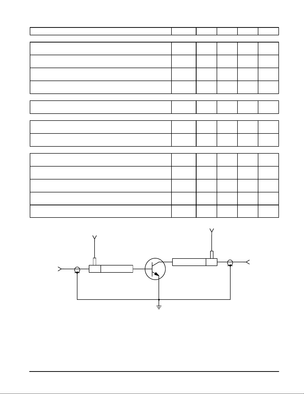
TYPICAL CHARACTERISTICS
Figure 2. fτ, Current–Gain Bandwidth Product
versus Collector Current
IC, COLLECTOR CURRENT (mA)
4020151051
7
0
Figure 3. Output Capacitance versus
Collector–Base Voltage
VCB, COLLECTOR–BASE VOLTAGE (VOLTS)
1010
2
1.5
0.5
0
Figure 4. Maximum Power Dissipation versus
Collector Lead Temperature (TC)
TC, CASE TEMPERATURE (°C)
150100755025
0
Figure 5. Forward Insertion Gain and
Maximum Unilateral Gain versus Frequency
f, FREQUENCY (GHz)
f
125 101
Figure 6. Forward Insertion Gain and
Maximum Unilateral Gain versus Frequency
f, FREQUENCY (GHz)
0.1
Figure 7. Minimum Noise Figure and
Associated Gain versus Frequency
f, FREQUENCY (GHz)
0.2
4
0
3.5
3
2.5
2
1.5
1
0.5
2000 0.1
1 10 0.3 0.5 1 32
6
5
4
3
2
1
30
C
cb
, C
ob
(pF)
1
2 3 4 5 6 7 8 9
300
250
200
150
100
50
P
D(max)
, MAXIMUM POWER DISSIPATION (mW)
G
Umax S
21
(dB)
2,
35
30
25
20
15
10
5
0
–5
G
Umax S
21
(dB)
2,
NF
min
, MINIMUM NOISE FIGURE (dB)
G
NF
, ASSOCIATED GAIN (dB)
20
18
16
14
12
10
8
6
4
τ
, GAIN BANDWIDTH PRODUCT (GHz)
0.2 0.5 2 3 50.3
0.2 0.3 0.5 2 3 5 0.1
Page 4
MRF917T1
4
MOTOROLA RF DEVICE DATA
VCE = 6 V
VCE = 3 V
VCE = 3 V
IC = 3 mA
NF
min
G
NF
Figure 8. Minimum Noise Figure and
Associated Gain versus Frequency
f, FREQUENCY (GHz)
0.1
4
0
3.5
3
2.5
2
1.5
1
0.5
0.2 0.3 0.5 1 32
NF
min
, MINIMUM NOISE FIGURE (dB)
G
NF
, ASSOCIATED GAIN (dB)
20
18
16
14
12
10
8
6
4
TYPICAL CHARACTERISTICS
5
1.5
4.5
4
3.5
3
2.5
2
NF
min
, MINIMUM NOISE FIGURE (dB)
IC, COLLECTOR CURRENT (mA)
1 3 5 10 3020
Figure 9. Minimum Noise Figure and
Associated Gain versus Collector Current
G
NF
, ASSOCIATED GAIN (dB)
14
12
10
8
6
4
2
0
5
1.5
4.5
4
3.5
3
2.5
2
NF
min
, MINIMUM NOISE FIGURE (dB)
IC, COLLECTOR CURRENT (mA)
1 3 5 10 3020
Figure 10. Minimum Noise Figure and
Associated Gain versus Collector Current
G
NF
, ASSOCIATED GAIN (dB)
14
12
10
8
6
4
2
0
2
2
NF
min
G
NF
NF
min
G
NF
Page 5

5
MRF917T1MOTOROLA RF DEVICE DATA
–j0.2
–j0.5
–j1.0
–j2.0
0.2
0.5 1.0 2.0
j1.0
j2.0j0.5
j0.2
j1.0
j2.0j0.5
j0.2
–j0.2
–j0.5
–j1.0
–j2.0
0.2
0.5 1.0 2.0
Γ
opt
10.0
10.8
2.4
1.7
2.2
1.8
2.5
14.0
12.0
1.6
Γ
opt
10.0
16.0
16.4
2.3
2.6
3.0
4.0
9.0
8.0
7.0
Figure 11. Constant Gain and Noise Figure Contours
— Potentially Unstable
f (MHz) NF OPT (dB) R
N
K
500 1.60 19 0.67
ΓMS NF OPT
0.39 é52°
VCE = 3.0 V
IC = 3.0 mA
Figure 12. Constant Gain and Noise Figure Contours
f (MHz) NF OPT (dB) R
N
K
1000 2.30 15 1.09
ΓMS NF OPT
0.29 é110°
VCE = 3.0 V
IC = 3.0 mA
Page 6

MRF917T1
6
MOTOROLA RF DEVICE DATA
Figure 13. Constant Gain and Noise Figure Contours
f (MHz) NF OPT (dB) R
N
K
500 1.70 19 0.80
ΓMS NF OPT
0.35 é45°
— Potentially Unstable
VCE = 6.0 V
IC = 5.0 mA
Figure 14. Constant Gain and Noise Figure Contours
f (MHz) NF OPT (dB) R
N
K
1000 2.3 16 1.09
ΓMS NF OPT
0.25 é99°
VCE = 6.0 V
IC = 5.0 mA
j1.0
j2.0j0.5
j0.2
–j0.2
–j0.5
–j1.0
–j2.0
0.2
0.5 1.0 2.0
2.2
18.6
1.7
Γ
opt
j1.0
j2.0j0.5
j0.2
–j0.2
–j0.5
–j1.0
–j2.0
0.2
0.5 1.0 2.0
9.0
5.0
3.0
4.0
12.0
11.5
10.5
Γ
opt
2.3
1.8
1.9
3.0
18.0
17.0
16.0
14.0
2.5
12.1
Page 7

7
MRF917T1MOTOROLA RF DEVICE DATA
VCE = 6 V
IC = 20 mA
THIRD ORDER INTERCEPT = +31 dBm
P
out
(–1 dB) = 14.5 dBm
VCE = 6 V
VCE = 3 V
Z
source
= 50
Ω
Z
load
= 50
Ω
Figure 15. Output Third Order Intercept
versus Collector Current
IC, COLLECTOR CURRENT (mA)
5
35
0
30
25
20
15
10
5
10 20 30 40
OUTPUT THIRD ORDER INTERCEPT (dBm)
+40
Pin, INPUT POWER (dBm)
–15
Figure 16. Third Order Intercept and 1 dB
Compression Point
P , OUTPUT POWER (dBm)
out
0
+35
+30
+25
+20
+15
+10
+5
–10 –5 0 5 10 15
V
CE
I
C
f (MHz) NF
min
(dB) |Gam Opt| ∠ Gam Opt R
N
3.0 V 1 mA 300 1.22 0.58 33 27
500 1.74 0.50 61 25
900 2.70 0.41 111 19
1000 2.93 0.40 121 18
1500 3.96 0.41 166 13
2000 4.83 0.54 –165 13
3 mA 300 1.25 0.46 26 20
500 1.57 0.39 52 19
900 2.19 0.30 100 16
1000 2.34 0.29 110 15
1500 3.08 0.31 158 13
2000 3.81 0.45 –165 11
6.0 V 3 mA 300 1.28 0.49 23 22
500 1.60 0.41 48 20
900 2.24 0.30 94 17
1000 2.39 0.29 104 16
1500 3.18 0.30 153 14
2000 3.97 0.43 –167 12
5 mA 300 1.45 0.41 21 20
500 1.68 0.35 45 19
900 2.17 0.26 89 16
1000 2.30 0.25 100 16
1500 2.96 0.26 149 13
2000 3.66 0.39 –167 12
10 mA 300 1.96 0.27 21 20
500 2.09 0.23 46 19
900 2.40 0.20 93 16
1000 2.49 0.19 104 16
1500 3.00 0.24 154 14
2000 3.60 0.36 –164 12
Table 1. MRF917T1 Common Emitter Noise Parameters
Page 8

MRF917T1
8
MOTOROLA RF DEVICE DATA
VIf
S
11
S
21
S
12
S
22
V
CE
(Volts)
I
C
(mA)
f
(GHz)
|S11|
∠Ăφ
|S21|
∠Ăφ
|S12|
∠Ăφ
|S22|
∠Ăφ
3.0 3.0 0.10 0.814 –38 9.28 152 0.040 70 0.921 –18
0.20 0.704 –69 7.56 132 0.066 56 0.784 –28
0.30 0.615 –91 6.11 117 0.081 49 0.677 –34
0.40 0.553 –109 5.01 106 0.091 46 0.602 –37
0.50 0.512 –122 4.24 98 0.098 45 0.552 –39
0.60 0.465 –134 3.59 92 0.104 44 0.510 –39
0.70 0.447 –144 3.16 86 0.110 45 0.487 –40
0.80 0.441 –151 2.79 81 0.117 45 0.472 –41
0.90 0.428 –159 2.54 77 0.123 46 0.457 –43
1.00 0.424 –165 2.32 72 0.129 47 0.447 –44
1.50 0.423 –170 1.64 55 0.167 51 0.420 –55
2.00 0.439 –152 1.30 40 0.211 52 0.413 –68
2.50 0.462 –135 1.09 28 0.263 51 0.407 –83
3.00 0.485 –122 0.95 19 0.321 48 0.406 – 98
4.00 0.543 –98 0.77 5 0.446 38 0.410 –133
5.0 0.10 0.717 –48 13.51 146 0.036 67 0.864 –24
0.20 0.589 –83 10.13 124 0.057 55 0.678 –36
0.30 0.511 –106 7.75 110 0.068 51 0.559 –41
0.40 0.463 –123 6.17 101 0.078 50 0.485 –43
0.50 0.436 –135 5.12 94 0.086 51 0.440 –44
0.60 0.400 –146 4.31 88 0.094 52 0.402 –42
0.70 0.390 –154 3.76 84 0.103 53 0.381 –43
0.80 0.389 –162 3.32 79 0.112 53 0.367 –44
0.90 0.381 –168 2.99 75 0.121 54 0.356 –45
1.00 0.380 –173 2.73 71 0.130 55 0.347 –46
1.50 0.388 –165 1.91 55 0.179 55 0.323 –56
2.00 0.406 –148 1.51 42 0.229 53 0.316 –68
2.50 0.431 –133 1.27 30 0.281 50 0.310 –83
3.00 0.456 –121 1.11 20 0.335 46 0.309 –98
4.00 0.519 99 0.90 4 0.446 36 0.322 –133
10 0.10 0.552 –67 19.98 136 0.031 63 0.752 –34
0.20 0.442 –105 13.19 114 0.045 57 0.523 –45
0.30 0.398 –127 9.51 103 0.056 58 0.413 –49
0.40 0.377 –142 7.37 95 0.067 59 0.351 –49
0.50 0.365 –151 6.02 89 0.078 61 0.317 –50
0.60 0.345 –162 5.05 85 0.089 62 0.284 –46
0.70 0.343 –168 4.37 81 0.100 62 0.269 –46
0.80 0.345 –174 3.86 77 0.112 62 0.258 –47
0.90 0.341 –179 3.46 74 0.123 62 0.250 –48
1.00 0.344 –177 3.14 70 0.135 62 0.243 –49
1.50 0.359 –159 2.19 56 0.192 59 0.223 –58
2.00 0.378 –144 1.72 43 0.248 54 0.216 –71
2.50 0.404 –130 1.44 32 0.301 49 0.210 –87
3.00 0.431 –119 1.26 22 0.352 44 0.210 –102
4.00 0.492 –99 1.03 5 0.452 33 0.227 –138
20 0.10 0.394 –94 25.51 125 0.024 64 0.612 –44
0.20 0.349 –131 15.10 106 0.037 64 0.387 –52
0.30 0.339 –148 10.51 97 0.049 66 0.301 –54
0.40 0.336 –159 8.03 91 0.062 68 0.255 –54
0.50 0.333 –165 6.50 86 0.075 68 0.232 –54
0.60 0.323 –175 5.44 82 0.088 69 0.204 –48
0.70 0.325 –179 4.70 79 0.100 68 0.194 –48
0.80 0.329 –176 4.14 75 0.113 68 0.185 –50
0.90 0.329 –173 3.71 72 0.126 67 0.180 –50
1.00 0.332 –169 3.36 69 0.139 66 0.175 –52
1.50 0.351 –154 2.33 56 0.201 61 0.160 –62
2.00 0.372 –141 1.82 44 0.258 55 0.155 –77
2.50 0.399 –128 1.53 33 0.313 50 0.151 –95
3.00 0.423 –118 1.34 24 0.364 44 0.152 –111
4.00 0.486 –98 1.09 7 0.459 32 0.174 –149
Table 2. MRF917T1 Common Emitter S–Parameters
Page 9

9
MRF917T1MOTOROLA RF DEVICE DATA
VIf
S
11
S
21
S
12
S
22
V
CE
(Volts)
I
C
(mA)
f
(GHz)
|S11|
∠Ăφ
|S21|
∠Ăφ
|S12|
∠Ăφ
|S22|
∠Ăφ
3.0 40 0.10 0.331 –127 26.91 116 0.020 67 0.480 –49
0.20 0.338 –154 14.86 100 0.033 70 0.297 –52
0.30 0.342 –164 10.16 93 0.046 72 0.239 –51
0.40 0.347 –171 7.70 88 0.060 73 0.210 –50
0.50 0.347 –175 6.22 84 0.074 73 0.196 –50
0.60 0.344 –177 5.21 80 0.087 73 0.176 –44
0.70 0.346 –174 4.49 77 0.100 72 0.171 –45
0.80 0.352 –170 3.96 74 0.114 71 0.164 –47
0.90 0.352 –167 3.54 71 0.127 70 0.161 –47
1.00 0.356 –164 3.21 68 0.140 69 0.157 –50
1.50 0.377 –151 2.23 55 0.202 63 0.145 –62
2.00 0.400 –138 1.75 43 0.261 57 0.142 –80
2.50 0.426 –126 1.47 33 0.317 50 0.139 –100
3.00 0.448 –115 1.29 23 0.369 44 0.141 –117
4.00 0.504 –96 1.06 7 0.465 32 0.166 –156
6.0 3.0 0.10 0.829 –34 9.23 154 0.033 71 0.936 –14
0.20 0.720 –63 7.67 134 0.056 59 0.823 –23
0.30 0.627 –85 6.30 120 0.069 52 0.730 –28
0.40 0.557 –102 5.21 109 0.078 49 0.664 –31
0.50 0.509 –115 4.44 101 0.085 47 0.619 –32
0.60 0.456 –127 3.77 94 0.091 47 0.581 –32
0.70 0.434 –137 3.32 88 0.096 47 0.561 –33
0.80 0.425 –145 2.93 83 0.102 48 0.547 –34
0.90 0.408 –153 2.67 79 0.108 49 0.534 –35
1.00 0.402 –160 2.44 75 0.114 50 0.524 –37
1.50 0.396 –174 1.72 57 0.148 54 0.501 –46
2.00 0.411 –155 1.36 43 0.189 56 0.494 –58
2.50 0.435 –137 1.14 31 0.237 56 0.485 –71
3.00 0.463 –123 0.99 21 0.294 54 0.482 –84
4.00 0.525 99 0.79 7 0.424 45 0.473 –117
5.0 0.10 0.736 –43 13.73 148 0.030 69 0.888 –20
0.20 0.602 –75 10.55 126 0.048 58 0.727 –29
0.30 0.512 –98 8.19 113 0.059 54 0.620 –33
0.40 0.454 –114 6.56 103 0.068 53 0.553 –35
0.50 0.418 –127 5.47 96 0.076 53 0.512 –35
0.60 0.377 –138 4.61 90 0.083 54 0.479 –34
0.70 0.363 –147 4.03 85 0.091 55 0.461 –34
0.80 0.359 –155 3.55 81 0.099 56 0.448 –35
0.90 0.348 –162 3.21 77 0.107 57 0.438 –36
1.00 0.346 –168 2.92 73 0.116 57 0.430 –37
1.50 0.351 –169 2.04 57 0.160 58 0.409 –46
2.00 0.370 –152 1.60 44 0.206 57 0.401 –57
2.50 0.398 –136 1.30 32 0.255 54 0.392 –69
3.00 0.425 –123 1.17 22 0.307 51 0.389 –82
4.00 0.496 –100 0.93 6 0.421 42 0.385 –113
10 0.100 0.547 –62 21.95 136 0.025 66 0.768 –29
0.200 0.417 –99 14.53 115 0.038 60 0.558 –37
0.300 0.362 –120 10.49 103 0.048 61 0.460 –38
0.400 0.334 –135 8.13 96 0.058 63 0.408 –38
0.500 0.319 –145 6.64 90 0.069 64 0.379 –38
0.600 0.294 –156 5.56 86 0.079 65 0.354 –34
0.700 0.291 –163 4.82 82 0.089 65 0.343 –34
0.800 0.293 –169 4.25 78 0.100 65 0.333 –35
0.900 0.290 –174 3.81 75 0.110 65 0.327 –36
1.000 0.292 –179 3.46 72 0.121 65 0.321 –37
1.500 0.307 –162 2.40 58 0.174 62 0.304 –45
2.000 0.330 –147 1.87 45 0.225 58 0.296 –56
2.500 0.359 –133 1.57 34 0.275 53 0.285 –68
3.000 0.387 –122 1.36 24 0.324 49 0.280 –80
4.000 0.461 –101 1.10 7 0.424 38 0.275 –112
Table 2. MRF917T1 Common Emitter S–Parameters (continued)
Page 10

MRF917T1
10
MOTOROLA RF DEVICE DATA
VIf
S
11
S
21
S
12
S
22
V
CE
(Volts)
I
C
(mA)
f
(GHz)
|S11|
∠Ăφ
|S21|
∠Ăφ
|S12|
∠Ăφ
|S22|
∠Ăφ
6.0 20 0.10 0.391 –85 27.76 125 0.020 66 0.637 –36
0.20 0.313 –122 16.43 106 0.032 66 0.436 –39
0.30 0.292 –140 11.44 98 0.043 68 0.365 –38
0.40 0.284 –152 8.74 91 0.055 70 0.330 –36
0.50 0.279 –159 7.08 87 0.067 70 0.313 –36
0.60 0.266 –169 5.92 83 0.078 71 0.295 –32
0.70 0.267 –174 5.11 80 0.090 70 0.289 –32
0.80 0.272 –179 4.50 76 0.101 70 0.281 –33
0.90 0.271 –177 4.03 73 0.113 69 0.278 –34
1.00 0.275 –173 3.65 71 0.124 68 0.274 –35
1.50 0.297 –158 2.52 58 0.179 64 0.260 –43
2.00 0.322 –144 1.97 46 0.232 58 0.251 –55
2.50 0.353 –131 1.64 35 0.283 53 0.239 –68
3.00 0.380 –120 1.43 25 0.332 48 0.233 –81
4.00 0.452 –100 1.16 8 0.430 37 0.225 –113
40 0.10 0.319 –114 27.96 116 0.017 67 0.532 –34
0.20 0.295 –145 15.39 101 0.029 71 0.391 –31
0.30 0.292 –157 10.51 93 0.040 73 0.353 –29
0.40 0.295 –165 7.98 88 0.052 74 0.335 –28
0.50 0.295 –170 6.45 85 0.064 74 0.327 –29
0.60 0.290 –179 5.39 81 0.076 74 0.316 –26
0.70 0.294 –178 4.65 78 0.087 73 0.313 –27
0.80 0.300 –174 4.10 75 0.099 72 0.306 –29
0.90 0.301 –171 3.67 72 0.110 71 0.305 –30
1.00 0.306 –168 3.33 69 0.121 70 0.301 –32
1.50 0.333 –154 2.31 57 0.176 65 0.286 –42
2.00 0.359 –141 1.81 45 0.229 60 0.276 –54
2.50 0.389 –127 1.52 34 0.281 55 0.262 –68
3.00 0.415 –117 1.32 25 0.332 50 0.254 –81
4.00 0.478 –97 1.08 8 0.434 38 0.241 –113
Table 2. MRF917T1 Common Emitter S–Parameters (continued)
Page 11

11
MRF917T1MOTOROLA RF DEVICE DATA
PACKAGE DIMENSIONS
CASE 419–02
ISSUE H
STYLE 3:
PIN 1. BASE
2. EMITTER
3. COLLECTOR
C
R
N
A
L
D
G
V
S
B
H
J
K
3
1 2
NOTES:
1. DIMENSIONING AND TOLERANCING PER ANSI
Y14.5M, 1982.
2. CONTROLLING DIMENSION: INCH.
DIM MIN MAX MIN MAX
MILLIMETERSINCHES
A 0.071 0.087 1.80 2.20
B 0.045 0.053 1.15 1.35
C 0.035 0.049 0.90 1.25
D 0.012 0.016 0.30 0.40
G 0.047 0.055 1.20 1.40
H 0.000 0.004 0.00 0.10
J 0.004 0.010 0.10 0.25
K 0.017 REF 0.425 REF
L 0.026 BSC 0.650 BSC
N 0.028 REF 0.700 REF
R 0.031 0.039 0.80 1.00
S 0.079 0.087 2.00 2.20
V 0.012 0.016 0.30 0.40
0.05 (0.002)
Page 12

MRF917T1
12
MOTOROLA RF DEVICE DATA
Motorola reserves the right to make changes without further notice to any products herein. Motorola makes no warranty , representation or guarantee regarding
the suitability of its products for any particular purpose, nor does Motorola assume any liability arising out of the application or use of any product or circuit, and
specifically disclaims any and all liability , including without limitation consequential or incidental damages. “Typical” parameters which may be provided in Motorola
data sheets and/or specifications can and do vary in different applications and actual performance may vary over time. All operating parameters, including “Typicals”
must be validated for each customer application by customer’s technical experts. Motorola does not convey any license under its patent rights nor the rights of
others. Motorola products are not designed, intended, or authorized for use as components in systems intended for surgical implant into the body, or other
applications intended to support or sustain life, or for any other application in which the failure of the Motorola product could create a situation where personal injury
or death may occur. Should Buyer purchase or use Motorola products for any such unintended or unauthorized application, Buyer shall indemnify and hold Motorola
and its officers, employees, subsidiaries, affiliates, and distributors harmless against all claims, costs, damages, and expenses, and reasonable attorney fees
arising out of, directly or indirectly, any claim of personal injury or death associated with such unintended or unauthorized use, even if such claim alleges that
Motorola was negligent regarding the design or manufacture of the part. Motorola and are registered trademarks of Motorola, Inc. Motorola, Inc. is an Equal
Opportunity/Affirmative Action Employer.
How to reach us:
USA/EUROPE/Locations Not Listed: Motorola Literature Distribution; JAPAN: Nippon Motorola Ltd.; Tatsumi–SPD–JLDC, 6F Seibu–Butsuryu–Center,
P.O. Box 20912; Phoenix, Arizona 85036. 1–800–441–2447 or 602–303–5454 3–14–2 Tatsumi Koto–Ku, Tokyo 135, Japan. 03–81–3521–8315
MFAX: RMFAX0@email.sps.mot.com – TOUCHTONE 602–244–6609 ASIA/PACIFIC: Motorola Semiconductors H.K. Ltd.; 8B Tai Ping Industrial Park,
INTERNET: http://Design–NET.com 51 Ting Kok Road, Tai Po, N.T., Hong Kong. 852–26629298
MRF917T1/D
*MRF917T1/D*
◊
 Loading...