

Page 1
SEMICONDUCTOR TECHNICAL DATA
The RF Line
Designed for 12.5 Volt UHF large–signal, common emitter, class–C amplifier
applications in industrial and commercial FM equipment operating to 520 MHz.
• Specified 12.5 Volt, 512 MHz Characteristics
Output Power = 65 Watts
Minimum Gain = 4.15 dB
Minimum Efficiency = 50%
• Characterized with Series Equivalent Large–Signal Impedance Parameters
from 400 to 520 MHz
• Built–In Matching Network for Broadband Operation
• Triple Ion Implanted for More Consistent Characteristics
• Implanted Emitter Ballast Resistors for Improved Ruggedness
• Silicon Nitride Passivated
• Capable of Surviving Load Mismatch Stress at all Phase Angles with
20:1 VSWR @ 15.5 Vdc and 2.0 dB Overdrive
Order this document
by MRF658/D
65 W, 512 MHz
RF POWER TRANSISTOR
NPN SILICON
MAXIMUM RATINGS
Rating Symbol Value Unit
Collector–Emitter Voltage V
Collector–Emitter Voltage V
Emitter–Base Voltage V
Collector Current — Continuous I
Total Device Dissipation @ TC = 25°C
Derate above 25°C
Storage Temperature Range T
THERMAL CHARACTERISTICS
Characteristic Symbol Max Unit
Thermal Resistance, Junction to Case R
ELECTRICAL CHARACTERISTICS (T
Characteristic Symbol Min Typ Max Unit
= 25°C unless otherwise noted.)
C
OFF CHARACTERISTICS
Collector–Emitter Breakdown V oltage
(IC = 50 mAdc, IB = 0)
Collector–Emitter Breakdown Voltage
(IC = 50 mAdc, VBE = 0)
Emitter–Base Breakdown Voltage
(IE = 10 mAdc, IC = 0)
Collector Cutoff Current
(VCE = 15 Vdc, VBE = 0, TC = 25°C)
V
(BR)CEO
V
(BR)CES
V
(BR)EBO
I
CES
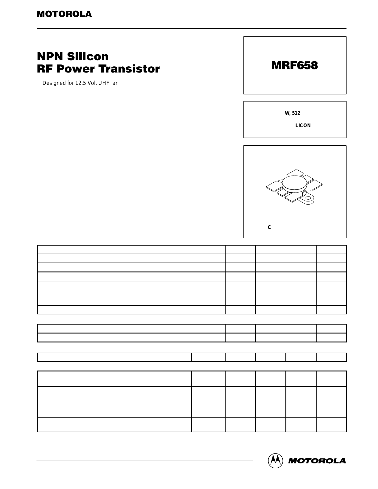
CASE 316–01, STYLE 1
CEO
CES
EBO
C
P
D
stg
θJC
16.5 29 — Vdc
38 45 — Vdc
4.0 4.6 — Vdc
— 0.1 10 mAdc
16.5 Vdc
38 Vdc
4.0 Vdc
15 Adc
175
1.0
– 65 to +150 °C
1.0 °C/W
Watts
W/°C
(continued)
REV 7
Motorola, Inc. 1997
MRF658MOTOROLA RF DEVICE DATA
1
Page 2
ELECTRICAL CHARACTERISTICS — continued (T
Characteristic Symbol Min Typ Max Unit
= 25°C unless otherwise noted.)
C
ON CHARACTERISTICS
DC Current Gain
(IC = 10 Adc, VCE = 5.0 Vdc)
DYNAMIC CHARACTERISTICS
Output Capacitance
(VCB = 12.5 Vdc, IE = 0, f = 1.0 MHz)
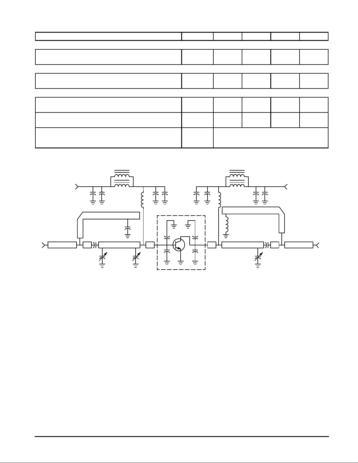
FUNCTIONAL TESTS (In Motorola Test Fixture. See Figure 1.)
Output Power
(VCC = 12.5 Vdc, Pin = 25 W, f = 470 & 512 MHz)
Collector Efficiency
(VCC = 12.5 Vdc, P
Output Mismatch Stress
(VCC = 15.5 Vdc, Pin = 32 W, f = 512 MHz, VSWR 20:1,
All Phase Angles)
= 65 W, f = 470 & 512 MHz)
out
h
FE
C
ob
P
out
η 50 60 — %
ψ No Degradation in Output Power
40 85 120 —
— 170 220 pF
65 — — W
B4
B3
L2
L3
C19
0.18 µF
C11
+
C12
12.5 Vdc
C20
10 µF
LOAD % = 50 OHMS
DELTA VRE PORT
(NORMALL Y SHOR TED)
C13
µ
F
10
RF INPUT RF OUTPUT
N1 N2
B1–B4 — Long Bead, Fair Rite (2743019446)
C1 — 56 pF , Chip Capacitor, Murata Erie
C2 — 1–20 pF Trimmer, Johanson–JMC 5501 PG26J200
C3 — 39 pF , Chip Capacitor, Murata Erie
C4 — 1–20 pF Trimmer, Johanson–JMC 5501
C5 — 33 pF , Miniature Clamped Mica, SAHA
C6 — 33 pF , Miniature Clamped Mica, SAHA
C7 — 33 pF , Miniature Clamped Mica, SAHA
C8 — 27 pF , Miniature Clamped Mica, SAHA
C11 — 1–20 pF Trimmer, Johanson–JMC 5501 PG26J200
C12 — 110 pF, Chip Capacitor, Murata Erie
C13 — 10 µF, 50 V Electrolytic, Panasonic–ECEV1HV100R
C14 — 0.18 µF Chip Capacitor
C15 — 130 pF, Chip Capacitor, Murata Erie
B1
B2
+
C14
0.18 µF
C3
C1
C2 C4
C15 C16 C17 C18
L1
SOCKET
D.U.T.
C5
C6
C16 — 130 pF, Chip Capacitor, Murata Erie
C17 — 130 pF, Chip Capacitor, Murata Erie
C18 — 130 pF, Chip Capacitor, Murata Erie
C19 — 0.18 µF Chip Capacitor
C20 — 10 µF, 50 V Electrolytic, Panasonic–ECEV1HV100R
Board — 1/16″ Glass Teflon, εr = 2.55, Keene (GX–0600–55–22)
L1, L2 — 5 Turns, 20 AWG, ID 0.126″
L3 — 2 Turns, 26 AWG, ID 0.073″
N1, N2 — Type N Flange, Omni Spectra (3052–1648–10)
Murata Erie Chip Capacitors —
GRH710COGxxxx100VBE
SAHA Mini Clamped Mica Capacitors — 3HS0006–xx
C7
C8
MRF658
2
Figure 1. 512 MHz Test Circuit
MOTOROLA RF DEVICE DATA
Page 3

110
100
90
80
70
60
50
40
, OUTPUT POWER (WATTS)
30
OUT
P
20
10
510 152025303540
PIN, INPUT POWER (WATTS)
f = 440 MHz
470
512
VCC = 12.5 Vdc
100
90
80
70
60
50
40
, OUTPUT POWER (WATTS)
30
OUT
P
20
10
PIN = 30 W
25 W
20 W
15 W
10 W
VCC = 12.5 Vdc
400 410 420 430 440 450 460 470 480 490 500 510 520 530
300
f, FREQUENCY (MHz)
Figure 2. Output Power versus Input Power
120
110
f = 512 MHz
100
90
80
70
60
50
40
, OUTPUT POWER (WATTS)
30
OUT
P
20
10
7 8 9 1011121314151617
VCC, SUPPLY VOLTAGE (VOLTS)
Figure 4. Output Power versus Supply Voltage
PIN = 35 W
Figure 3. Output Power versus Frequency
30 W
25 W
20 W
15 W
10 W
MRF658MOTOROLA RF DEVICE DATA
3
Page 4

+j10
+j5
520
460
f = 400 MHz
+j2
0
2 5 10 20 30 50
Z
IN
VCC = 12.5 V Po = 70 W
f
MHz
400
440
480
520
0.62 + j2.8
0.72 + j3.1
0.81 + j3.3
0.90 + j3.6
Zo = 10
ZIN
OHMS
Ω
ZOL*
OHMS
1.20 + j2.5
1.10 + j2.8
0.94 + j3.1
0.80 + j3.4
+j20
+j30
+j50
+j100
0
+j2
+j10
+j5
520
460
f = 400 MHz
2 5 10 20 30 50
Z
OL*
Zo = 10
Ω
ZOL* = Conjugate of optimum load impedance into
ZOL* = which the device operates at a given output
ZOL* = power, voltage and frequency.
Figure 5. Series Equivalent Input and Output Impedances
+j20
+j30
+j50
+j100
MRF658
4
MOTOROLA RF DEVICE DATA
Page 5

P ACKAGE DIMENSIONS
D
R
Q
J
E
F
4
3
1
2
K
L
B
H
A
C
N
STYLE 1:
PIN 1. EMITTER
U
NOTES:
1. FLANGE IS ISOLATED IN ALL STYLES.
DIM MIN MAX MIN MAX
A 24.38 25.14 0.960 0.990
B 12.45 12.95 0.490 0.510
C 5.97 7.62 0.235 0.300
D 5.33 5.58 0.210 0.220
E 2.16 3.04 0.085 0.120
F 5.08 5.33 0.200 0.210
H 18.29 18.54 0.720 0.730
J 0.10 0.15 0.004 0.006
K 10.29 11.17 0.405 0.440
L 3.81 4.06 0.150 0.160
N 3.81 4.31 0.150 0.170
Q 2.92 3.30 0.115 0.130
R 3.05 3.30 0.120 0.130
U 11.94 12.57 0.470 0.495
2. COLLECTOR
3. EMITTER
4. BASE
MILLIMETERSINCHES
CASE 316–01
ISSUE D
MRF658MOTOROLA RF DEVICE DATA
5
Page 6

Motorola reserves the right to make changes without further notice to any products herein. Motorola makes no warranty , representation or guarantee regarding
the suitability of its products for any particular purpose, nor does Motorola assume any liability arising out of the application or use of any product or circuit,
and specifically disclaims any and all liability, including without limitation consequential or incidental damages. “T ypical” parameters can and do vary in different
applications. All operating parameters, including “T ypicals” must be validated for each customer application by customer’s technical experts. Motorola does
not convey any license under its patent rights nor the rights of others. Motorola products are not designed, intended, or authorized for use as components in
systems intended for surgical implant into the body, or other applications intended to support or sustain life, or for any other application in which the failure of
the Motorola product could create a situation where personal injury or death may occur. Should Buyer purchase or use Motorola products for any such
unintended or unauthorized application, Buyer shall indemnify and hold Motorola and its officers, employees, subsidiaries, affiliates, and distributors harmless
against all claims, costs, damages, and expenses, and reasonable attorney fees arising out of, directly or indirectly, any claim of personal injury or death
associated with such unintended or unauthorized use, even if such claim alleges that Motorola was negligent regarding the design or manufacture of the part.
Motorola and are registered trademarks of Motorola, Inc. Motorola, Inc. is an Equal Opportunity/Af firmative Action Employer.
Literature Distribution Centers:
USA: Motorola Literature Distribution; P.O. Box 20912; Phoenix, Arizona 85036.
EUROPE: Motorola Ltd.; European Literature Centre; 88 T anners Drive, Blakelands, Milton Keynes, MK14 5BP, England.
JAPAN: Nippon Motorola Ltd.; 4-32-1, Nishi-Gotanda, Shinagawa-ku, Tokyo 141, Japan.
ASIA PACIFIC: Motorola Semiconductors H.K. Ltd.; Silicon Harbour Center , No. 2 Dai King Street, T ai Po Industrial Estate, Tai Po, N.T., Hong Kong.
MRF658
6
◊
MOTOROLA RF DEVICE DATA
MRF658/D
*MRF658/D*
 Loading...