

SEMICONDUCTOR TECHNICAL DATA
The RF Line
Order this document
by MRF653/D
Designed for 12.5 Volt UHF large–signal amplifier applications in industrial
and commercial FM equipment operating to 512 MHz.
• Specified 12.5 Volt, 512 MHz Characteristics
Output Power = 10 W
Gain = 8.0 dB (Typ)
Efficiency = 65% (Typ)
• Gold Metallized, Emitter Ballasted for Long Life and Reliability
• Capable of 20:1 VSWR Load Mismatch at 16 V Supply Voltage
• Circuit board photomaster available upon request by contacting
RF Tactical Marketing in Phoenix, AZ.
MAXIMUM RATINGS
Rating Symbol Value Unit
Collector–Emitter Voltage V
Collector–Base Voltage V
Emitter–Base Voltage V
Collector Current — Continuous I
Total Device Dissipation @ TA = 25°C
Derate above 25°C
Storage Temperature Range T
Operating Junction Temperature T
CEO
CBO
EBO
C
P
D
stg
J
THERMAL CHARACTERISTICS
Characteristic Symbol Max Unit
Thermal Resistance, Junction to Case R
ELECTRICAL CHARACTERISTICS (T
Characteristic
= 25°C unless otherwise noted)
C
OFF CHARACTERISTICS
Collector–Emitter Breakdown V oltage (IC = 20 mAdc, IB = 0) V
Collector–Emitter Breakdown Voltage (IC = 20 mAdc, VBE = 0) V
Emitter–Base Breakdown Voltage (IE = 5.0 mAdc, IC = 0) V
Collector Cutoff Current (VCE = 15 Vdc, VBE = 0) I
ON CHARACTERISTICS
DC Current Gain (IC = 1.0 Adc, VCE = 5.0 Vdc) h
DYNAMIC CHARACTERISTICS
Output Capacitance (VCB = 12.5 Vdc, IE = 0, f = 1.0 MHz) C
FUNCTIONAL TESTS
Common–Emitter Amplifier Power Gain
(VCC = 12.5 Vdc, P
Collector Efficiency
(VCC = 12.5 Vdc, P
Load Mismatch Stress
(VCC = 16 Vdc, f = 512 MHz, Pin (1) = 2.6 W,
VSWR = 20:1, All Phase Angles)
NOTE:
1. Pin = 2.0 dB over the typical input power required for 10 W output power @ 12.5 Vdc.
REV 8
= 10 W, f = 512 MHz)
out
= 10 W, f = 512 MHz)
out
16.5 Vdc
38 Vdc
4.0 Vdc
2.75 Adc
44
0.25
–65 to +150 °C
200 °C
Watts
W/°C
Symbol Min Typ Max Unit
(BR)CEO
(BR)CES
(BR)EBO
CES
FE
ob
G
pe
η
c
ψ
θJC
10 W, 512 MHz
RF POWER
TRANSISTOR
NPN SILICON
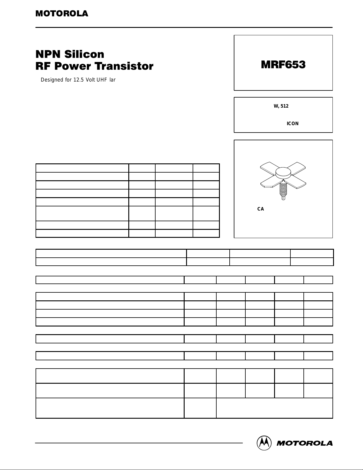
CASE 244–04, STYLE 1
4.0 °C/W
16.5 — — Vdc
38 — — Vdc
4.0 — — Vdc
— — 5.0 mAdc
20 — 120 —
— 22 28 pF
7.0 8.0 — dB
55 65 — %
No Degradation in Output Power
Motorola, Inc. 1997
MRF653MOTOROLA RF DEVICE DATA
1
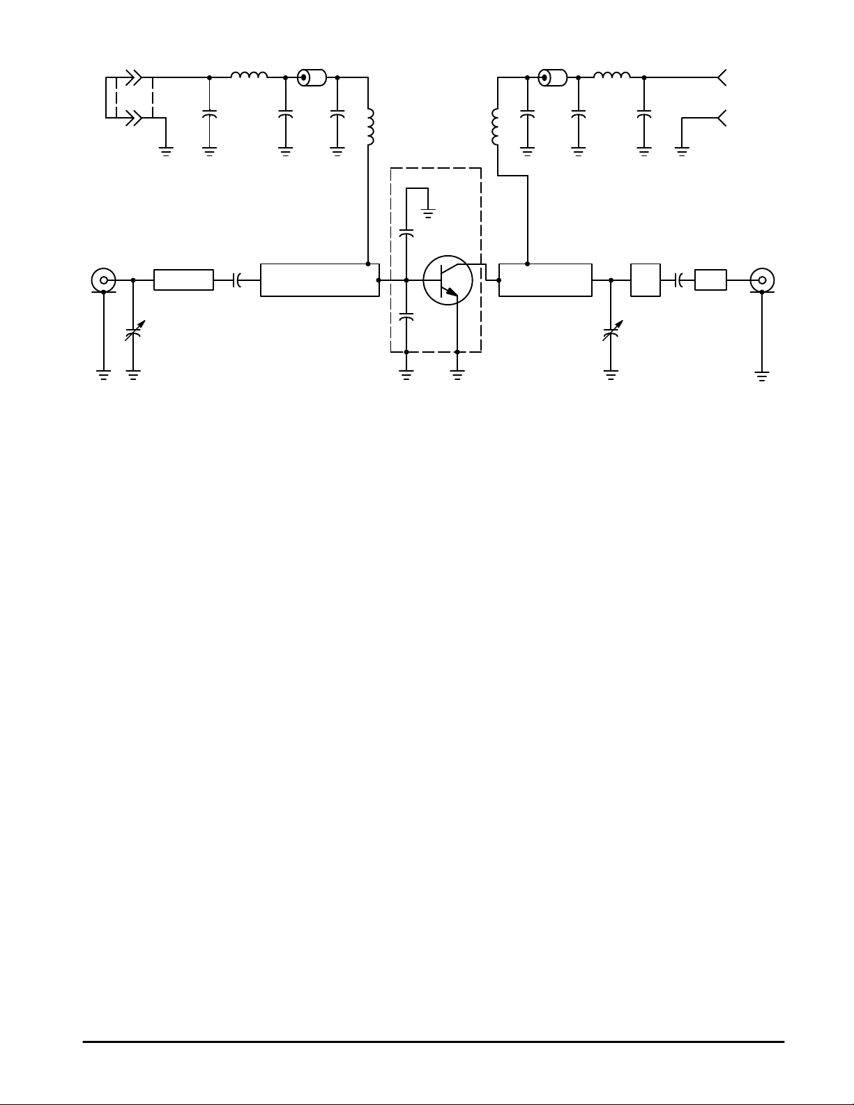
JP1
L1 L4
+
C7 C8 C9
L2 L3
SOCKET
C3
D.U.T.
C10
BB
C11 C12
+
+
V
CC
–
C2
C1
C1, C5 — 1.0–20 pF, Johanson
C2, C6 — 330 pF, 100 Mil ATC
C3, C4 — 36 pF, Mini–Unelco
C7, C12 — 10 µF, 35 V, Tantalum
C8, C11 — 0.1 µF, Ceramic
C9, C10 — 91 pF, Mini–Unelco
Z2Z1 Z4 Z5
C4
L1, L4 — 4–1/2 Turns, #18 AWG, 0.16″ ID
L2, L3 — 2 Turns, #18 AWG, 0.16″ ID
B — Ferrite Bead, Ferroxcube 56–590–65–3B
Z1 — 51 x 630 mils
Z2 — 162 x 1300 mils
Z3 — 210 x 1350 mils
Z4 — 210 x 280 mils
Z5 — 51 x 300 mils
Board Material — 0.032″ epoxy glass G10, 1 oz., copper clad,
Board Material — double sided, εr = 5
JP1 — Jumper, #14 AWG w/Banana Plugs
Z3
C6
C5
Figure 1. Broadband T est Circuit Schematic
MRF653
2
MOTOROLA RF DEVICE DATA

16
14
12
10
440 MHz
470
512
16
14
12
10
Pin = 2.4 W
1.6 W
8
6
4
out
P , OUTPUT POWER (WATTS)
2
0
0 0.5 2 3
1 1.5 2.5 3.5
Pin, INPUT POWER (WATTS)
VCC = 12.5 Vdc
8
6
4
out
P , OUTPUT POWER (WATTS)
2
0
430 440 470 490
VCC = 12.5 Vdc
450 460 480 500 510 520 530
f, FREQUENCY (MHz)
Figure 2. Output Power versus Input Power Figure 3. Output Power versus Frequency
16
14
12
10
8
6
4
out
P , OUTPUT POWER (WATTS)
2
0
6 8 10 12 14 16
fo = 512 MHz
7 9 11 13 15
VCC, SUPPLY VOLTAGE (VOLTS)
Pin = 2.4 W
1.6 W
0.8 W
10
G
8
6
4
, POWER GAIN (dB)
pe
G
2
0
440 460 480 520
450 470 510490
pe
η
c
VSWR
f, FREQUENCY (MHz)
0.8 W
P
= 10 W
out
VCC = 12.5 Vdc
500
70%
60%
50%
40%
1.3:1
1.2:1
1.1:1
, COLLECTOR EFFICIENCY
c
η
VSWR
Figure 4. Output Power versus Supply V oltage Figure 5. Typical Broadband Circuit Performance
MRF653MOTOROLA RF DEVICE DATA
3

f = 520 MHz
500
470
440
f = 520 MHz
Z
in
ZOL*
500
470
440
P
= 10 W, VCC = 12.5 Vdc
out
f (MHz) Z
440 1.0 + j2.2 4.3 – j2.8
470 1.0 + j2.4 4.4 – j2.1
500 1.0 + j2.6 4.1 – j1.7
520 1.0 + j2.7 3.9 – j1.65
ZOL* = Conjugate of the optimum load impedance
ZOL* = into which the device operates at a given
ZOL* = output power, voltage and frequency.
in
Zo = 10
Ω
ZOL*
MRF653
4
Figure 6. Series Equivalent Input and Output Impedance
MOTOROLA RF DEVICE DATA

P ACKAGE DIMENSIONS
2
T
F
P
8–32 NC 2A
WRENCH FLAT
4
A
13
K
M
SEATING PLANE
U
E
B
D
J
S
CASE 244–04
ISSUE J
DIM MIN MAX MIN MAX
A 7.06 7.26 0.278 0.286
B 6.20 6.50 0.244 0.256
C 14.99 16.51 0.590 0.650
D 5.46 5.96 0.215 0.235
E 1.40 1.65 0.055 0.065
G 1.52 ––– 0.060 –––
J 0.08 0.17 0.003 0.007
K 11.05 ––– 0.435 –––
M 45 NOM 45 NOM
__
C
P ––– 1.27 ––– 0.050
S 3.00 3.25 0.118 0.128
T 1.40 1.77 0.055 0.070
U 2.92 3.68 0.115 0.145
STYLE 1:
PIN 1. EMITTER
2. BASE
3. EMITTER
4. COLLECTOR
INCHESMILLIMETERS
MRF653MOTOROLA RF DEVICE DATA
5

Motorola reserves the right to make changes without further notice to any products herein. Motorola makes no warranty , representation or guarantee regarding
the suitability of its products for any particular purpose, nor does Motorola assume any liability arising out of the application or use of any product or circuit, and
specifically disclaims any and all liability, including without limitation consequential or incidental damages. “T ypical” parameters which may be provided in Motorola
data sheets and/or specifications can and do vary in different applications and actual performance may vary over time. All operating parameters, including “Typicals”
must be validated for each customer application by customer’s technical experts. Motorola does not convey any license under its patent rights nor the rights of
others. Motorola products are not designed, intended, or authorized for use as components in systems intended for surgical implant into the body, or other
applications intended to support or sustain life, or for any other application in which the failure of the Motorola product could create a situation where personal injury
or death may occur. Should Buyer purchase or use Motorola products for any such unintended or unauthorized application, Buyer shall indemnify and hold Motorola
and its officers, employees, subsidiaries, affiliates, and distributors harmless against all claims, costs, damages, and expenses, and reasonable attorney fees
arising out of, directly or indirectly, any claim of personal injury or death associated with such unintended or unauthorized use, even if such claim alleges that
Motorola was negligent regarding the design or manufacture of the part. Motorola and are registered trademarks of Motorola, Inc. Motorola, Inc. is an Equal
Opportunity/Affirmative Action Employer.
How to reach us:
USA/EUROPE/Locations Not Listed: Motorola Literature Distribution; JAPAN: Nippon Motorola Ltd.: SPD, Strategic Planning Office, 4–32–1,
P.O. Box 5405, Denver, Colorado 80217. 303–675–2140 or 1–800–441–2447 Nishi–Gotanda, Shinagawa–ku, Tokyo 141, Japan. 81–3–5487–8488
Mfax: RMFAX0@email.sps.mot.com – TOUCHTONE 602–244–6609 ASIA/PACIFIC: Motorola Semiconductors H.K. Ltd.; 8B Tai Ping Industrial Park,
– US & Canada ONLY 1–800–774–1848 51 Ting Kok Road, T ai Po, N.T., Hong Kong. 852–26629298
INTERNET: http://motorola.com/sps
Mfax is a trademark of Motorola, Inc.
MRF653
6
◊
MOTOROLA RF DEVICE DATA
MRF653/D
 Loading...