

Page 1
140 COMMERCE DRIVE
MONTGOMERYVILLE, PA
18936-1013
PHONE: (215) 631-9840
FAX: (215) 631-9855
RF & MICROWAVE DISCRETE
LOW POWER TRANSISTORS
Features
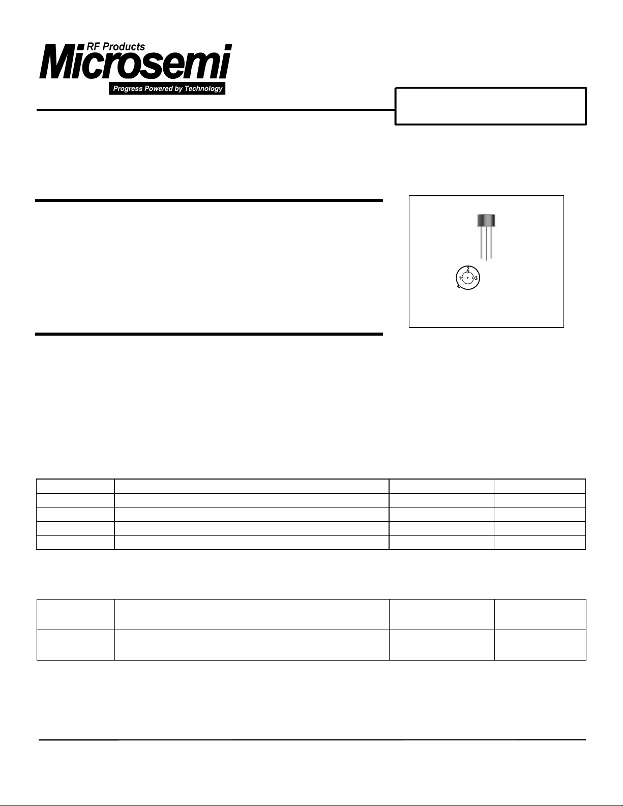
• Silicon PNP, high Frequency, high breakdown, To-39 packaged,
Transistor
MRF545
• Maximum Unilateral Gain = 14 dB (typ) @ f = 200 MHz
• High Collector Base Breakdown Voltage - BVCBO = 100 V (min)
• High FT - 1400 MHz
1. Emitter
2. Base
3. Collector
TO-39
DESCRIPTION:
Designed primarily for use in high frequency and medium and high resolution color video display monitors as well as other
applications requiring high breakdown characteristics.
ABSOLUTE MAXIMUM RATINGS (Tcase = 25°C)
Symbol Parameter Value Unit
V
CEO
V
CBO
V
EBO
I
C
Collector-Emitter Voltage 70 Vdc
Collector-Base Voltage 100 Vdc
Emitter-Base Voltage 3.0 Vdc
Collector Current 400 mA
Thermal Data
P
D
Tstg
MSC1315.PDF 10-25-99
Total Device Dissipation @ TA = 25ºC
Derate above 25ºC
Storage Temperature Range
3.5
20
-65 to +200
Watts
mW/ ºC
ºC
Page 2
ELECTRICAL SPECIFICATIONS (Tcase = 25°C)
STATIC
(off)
Symbol Test Conditions Value
Min. Typ. Max. Unit
BVCEO Collector-Emitter Breakdown Voltage
(IC = 1.0 mAdc, IB = 0) 70 - - Vdc
BVCBO Collector-Base Breakdown Voltage
(IC= 100 µAdc, IE=0)
BVEBO Emitter-Base Breakdown Voltage
(IE = 100 µAdc, IC = 0)
ICBO Collector Cutoff Current
(VCE = 80 Vdc, IE = 0 Vdc) - - 20
ICES Collector Cutoff Current
(VCE = 80 Vdc, IE = 0 Vdc) - 1.0 100
100 - - Vdc
3.0 - -
MRF545
Vdc
µA
µA
(on)
DYNAMIC
HFE DC Current Gain
(IC = 50 mAdc, VCE = 6.0 Vdc) 15 - -
Symbol Test Conditions Value
Min. Typ. Max. Unit
Output Capacitance
COB
CIB
CCB
f
T
(VCB = 10Vdc, IE=0, f=1 MHz) - 2.5 - pF
Input Capacitance
(VEB = 3Vdc, IE=0, f=1 MHz) - 5.4 - pF
Junction Capacitance
(VCB = 10Vdc, IE=0, f=1 MHz) - 2.8 3.2 pF
Current-Gain - Bandwidth Product
(IC = 50 mAdc, VCE = 25 Vdc, f = 250 MHz) 1000 1400 - MHz
MSC1315.PDF 10-25-99
Page 3

FUNCTIONAL
Symbol Test Conditions Value
Min. Typ. Max. Unit
G
U max
Maximum Unilateral Gain
IC = 50 mAdc, VCE = 25Vdc,
f = 200 MHz
- 14
MRF545
-
dB
MAG Maximum Available Gain
|S21|
2
Insertion Gain
Table 1. Common Emitter S-Parameters, @ VCE = 25 V, IC = 50 mA
(MHz) |S11|
100
200
300
400
500
600
700
800
900
1000
0.139 -105 7.43 101 0.031 83 0.573 -19
0.162 -168 4.35 80 0.066 82 0.508 -23
0.522 130 1.7 75 0.113 85 0.493 -29
0.260 129 2.23 63 0.154 85 0.487 -43
0.275 133 1.74 54 0.188 71 0.445 -53
0.262 123 1.49 46 0.226 74 0.495 -69
0.333 118 0.951 45 0.925 75 0.456 -71
0.327 122 1.3 35 0.379 66 0.424 -85
0.517 97 1.21 30 0.402 61 0.393 -109
0.463 115 1.07 27 0.437 63 0.375 -115
∠ φ
IC = 50 mAdc, VCE = 25Vdc,
f = 200 MHz
IC = 50 mAdc, VCE = 25Vdc,
f = 200 MHz
|S21|
∠ φ
- 14.5
11.5 12.5 - dB
|S12|
∠ φ
|S22|
-
dB
∠ φ
MSC1315.PDF 10-25-99
Page 4

MRF545
MSC1315.PDF 10-25-99
 Loading...